Realisation
of
analogue divider using current
feedback amplifiers
S.4. Liu J.-J. Chen
Indexing terms: Analogue circuits, Divider circuits
A b c t : New analogue divider circuits using current feedback amplifiers (CFAs) are presented. Basically, they consist of two CFAs, two MOS transistors biased in the triode region, and a resistor. Furthermore, an integrable divider circuit is also presented. Experimental results are given to demonstrate the feasibility of the proposed circuits. The proposed divider will be useful in high-frequency analogue signal processing.
1 Introduction
An
analogue divider is an important building block in analogue computation, fuzzy control and instrumen- tation, etc. [l-31. Many analogue continuous-time and sampled-data divider circuits have been presented in the literature [4-81. Most of them have used conventional operational amplifiers as building blocks to synthesise the division function. However, the finite-gain-bandwidth product of the operational amplifiers will limit the high- frequency operation and accuracy of the divider.Current-mode circuits have been receiving significant attention in analogue signal processing circuits [SI. A new amplifier called the current feedback amplifier (CFA) [lo, 113 has been realised to circumvent the finite-gain- bandwidth limitation of the conventional operational amplifier. It can provide not only constant bandwidth independent of the closed-loop gain but also high slew rate (i.e. 2000 V / p ) [ll]. It can be also used as a second- generation current conveyor (CCII) [12] by using its compensation node [13]. Moreover, since a CFA was built with a voltage buffer, it can drive external loads easily. In this paper we propose new analogue division circuits using CFAs. Experimental results are also given to verify the theoretical analysis.
2 Circuit description
The simplified equivalent circuit and symbol for a current feedback amplifier (CFA) are shown in Fig. la and b, respectively. This circuit is equivalent to a CCll with a
1
0 IEE, 1995
Paper 1609G (ElO), reaived 23rd February 1994
S.4. Liu is with the Department of Eledrical Engineering, National Taiwan University, Taipei, Taiwan 10664, Republic of China, on leave from the National Taiwan Institute of Technology
J.-J. Chen is with the Department of Electrical Enginming, National Taiwan University, Taipei, Taiwan 10664, Republic of China IEE hoc.-Circuits Devices Syst., Vol. 142, No. 1, February 1995
b
Fig. 1 Equivalent circuit for a current feedback amplifier
voltage buffer [12]. Its characteristics can be modelled as
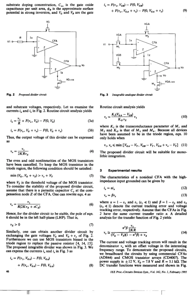
The proposed analogue division circuit with two CFAs is shown in Fig. 2. It consists of two CFAs, two NMOS transistors biased in the triode region and a resistor. The drain current of an NMOS transistor biased in the triode region can be expressed by [14]
with
where ID is the drain current in the triode region, W and L are the channel length and width, respectively, p is the effective mobility, V,, is the flatband voltage,
N,
is the 45substrate doping concentration, CO, is the gate oxide
capacitance per unit area,
Qs
is the approximate surface i, = F(vl, VGB) - F(0,VGB)
potential in strong inversion, and VG and V' are the gate
+
F(vo, VGA+
VX)-
F(0, VGA+
v x )- - M A v1
$-vGA+vx
-P
T T R I x - - = -vo&
' ; 1 ~
VG. vx & -Fig. 2 Proposed diuider circuit
and substrate voltages, respectively. Let us examine the currents i, and i, in Fig. 2. Routine circuit analysis yields
( 3 4
i, = F(v,
,
VG+
v,) - F(0, VG+
v,) ( 3 4Thus,
the output voltage of this divider can be expressed asV 1
v, = ~
ZKRv, (4)
The even and odd nonlinearities of the MOS transistors have been cancelled. To keep the MOS transistor in the triode region, the following condition should be satisfied:
min(VG,VG+vX)>v,+ V, (5)
where V, is the threshold voltage of the MOS transistor. To consider the stability of the proposed divider circuit, assume that there is a parasitic capacitor C , at the com- pensation node 2 of the CFA. One can rewrite eqn. 4 as
(9)
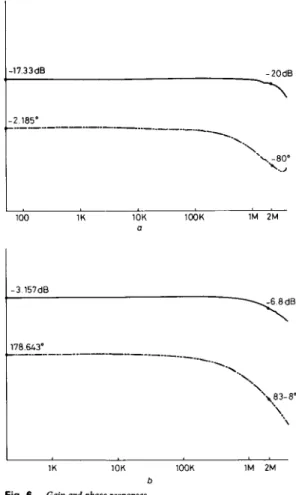
Routine circuit analysis yields
KI(VGA - VGB)
KO vx (10)
v, = V 1
where
K,
is the transconductance parameter of Ml andM , and K O is that of M , and M4. Because all devices have been assumed to be in the triode region, e q a 10 only holds when
V l r
<
min [VGA - V', VGB - V', VGA+
v x - VT'1 ( 1 1)The proposed divider circuit will be suitable for mono- lithic integration.
3 Experimental results
The characteristics of a nonideal CFA with the high- impedance input grounded can be given by
i, = ai, (12)
vo = Bvz (13)
V 1
R(2KvX
+
SC,)where a = 1 - and cl (cl 4 1) and = 1
-
E~ and c2( E ~ 4 1) denote the current tracking error and voltage tracking error, respectively. Assume that the CFAs in Fig.
2 have the same current transfer ratio a. A detailed
analysis for the transfer function of Fig. 2 yields v, =
Hence, for the divider circuit to be stable, the pole of eqn. 6 should be in the left half-plane
(LHP).
That is,V X
>
0 (7)Similarly, one can obtain another divider circuit by exchanging the gate voltages VG and VG
+
U, of Fig. 2. Furthermore we can use MOS transistors biased in the triode region to replace the passive resistor [4, 14, 151. The proposed integrable divider was shown in Fig. 3. We can express the currents i, and i, in Fig. 3 asi x = F(vi, VGA) - F(O, VG.J
+
F(vo, VGA)-
F(o, VGA) (8)(14)
The current and voltage tracking errors will result in the denominator v x with an offset voltage in the interesting frequency range. To demonstrate the proposed circuits, we breadboard the circuits by using commercial CFAs (AD844) and CMOS transistor arrays (CD4007). The power supply is & 12 V, VG = 7.8 V and R = 5.1
kR.
The DC transfer functions were measured and shown in Fig.46 IEE hoc.-Circuits Devices Syst., Vol. 142, No. I , February 199s
4a and b. The horizontal variable is U, and the vertical one is U,. Fig. 4a and b show the U, - U, transfer curve with u1 = 1.1 V and u1 = - 1.1 V, respectively. A ramp
signal with a positive slope was applied to o x , and Fig. 5 shows the time domain response of the proposed divider circuit. The frequency response of the proposed divider
a
I .
100 1K 10K lOOK 1M 2M
a
b b
Fig. 4 Tianger functions Fig. 6 Gain and phase responses
DC trander function against of proposed divider circuit with = v, a Gain (10 d B / W and phase (45"/div) r-ponm of proposd divider ( v . / ~ J with
DC transfer funnioo against of proposed divider circuit with = consfant U,(= 1.1 V). Upper @a= is gain repon= and lower one phase =pow circuit was also measured in Fig. 6a and b. Fig. 6a shows the frequency response of u1 against U, with U, = 1.1 V. Its -3 dB bandwidth was about 2 MHz. Fig. 66 shows the frequency response of U, against U, with u1 = 1.1 V. Its -3 dB bandwidth was about 1.8 MHz.
v, = 7.8 V and R = 5.1 kR. Horizontal scale is 1 and vertical scale is 0.2 b Gain (IO dB/div) and phase (45"/div) v)' trace is gain responses of proposed response and lower One divider phase rcspow (UJU,) with
div
- 1.1 V, V, = 7.8 V and R = 5.1 kn. Horizontal scale is 1 V/div and vertical scale
is 0.2 V/div
4 Conclusions
New analogue division circuits using CFAs have been proposed. Experimental results are given to demonstrate the feasibility of the proposed circuits. The divider circuit has a simple structure. Frequency responses show that the proposed divider will be useful in high-frequency ana- logue signal processing applications.
Fig. 5 Ramp signal and output voltage ~~ 5 References
Lower trace (1 Vjdiv) is ramp signal of .U and upper trace (0.2 V/div) is output voltage V, of divider. Horizontal scale is 0.5 ms/div
IEE Proc.-Circuits Devices Syst., Vol. J42, No. J , February 1995
1 MEAD, C., and ISMAIL, M.: 'Analog VLSI implementation of
neural systems' (Kluwer Academic, Boston, 1989)
...
2 SHEINGOLD, D.H. (Ed.): ‘Nonlinear circuit handbook‘ (Analog Devices, Norwood, MA, 1974)
3 YAMAKAWA, T.: ‘High-speed fuzzy controller hardware system: the Mega-FIPS machine’, In/: Sci., 1988,45, pp. 113-128
4 KHACHAB, N.I., and ISMAIL, M.: ‘A nonlinear CMOS analog a l l for VLSl signal and information processing’, IEEE J . Solid-
State Circuits, 1991.26, pp. 1689-1698
5 GHOSH, D., and PATRANABIS, D.: ‘A simple analog divider
having independent control of sensitivity and design condition’,
IEEE Trans., 1990, IM-39, pp. 522-526
6 LAOPPOULOS, TH. L., and KARYBAKAS, C.A.: ‘A simple
analog division scheme’, IEEE Trans., 1991, IM-40, pp. 779-782 7 ARONHIME, P., DESAI, M., and STEPHENS, J.: ‘Quotient cir-
cuits employing WR, IEEE Trans., 1992, IMM-41, pp. 679-684
8 LIU, S.I., WU, D.S., TSAO, H.W., WU, J., and TSAY, J.H.: ‘Non- linear circuit applications with current conveyors’, I E E Proc. G,
1993,140, pp. 1-6
48
9 WILSON, B.: ‘Recent developments in current conveyors and
current-mode circuits’, I E E Proc. G, 1990,137, (2). pp. 63-77 10 ‘Linear products data book‘ (Analog Devices, Norwood, MA, 1990) 11 ‘Designer’s guide for 200 series o p amp’. Application note 2W1
(Comlinear Corporation, 4800 Wheaton Drive, Ft. Collins, C O 80525, November 1984)
12 SEDRA, A., and SMITH, K.C.: ‘A second generation current con-
veyor and its applications’, IEEE Trans., 1970,CT-17, pp. 132-134
13 SVOBODA, J.A., McGORY, L., and WEBB, S.: ‘Applications of a
commercially available current conveyor’, Int. J. Electron., 1991, pp. 14 BANU, M., and TSIVIDIS, Y.: ‘Detailed analysis of nonlinearities in MOS fully integrated active RC filters based on balanced net- works’, IEE Proc. G, 1984,134, pp. 190-196
15 ZARNUL, C.: ‘Novel MOS resistive circuit for synthesis of fully
integrated continuous-time filters’, IEEE Trans., 1986, CAS-33, pp.
718-721 159-164