Design and Fabrication of Multilayer HTS Filters
K. Chen1, S. H. Tsai2, J. H. Horng3, and C. Y. Huang4
1Materials Research Laboratories, Industrial Technology Research Institute,
Chutung, Hsinchu, Taiwan 310, R.O.C.
2Department of Physics, National Tsing Hua University, Hsinchu, Taiwan 202, R.O.C. 3Department of Mechanical and Marine Engineering, National Ocean University, Taiwan 300, R.O.C.
4Center for Condensed Matter Science, National Taiwan University, Taipei 106, R.O.C
(Received August 17, 1999)
A multilayer HTS band-pass filter has been designed and fabricated. Tapped combline filters with multilayer structure were designed. The center of frequency of the pass band is at 1.9 GHz with band width of 50 MHz. YBCO thin films deposited on LaAlO3 substrates
were used to construct the filter. Wet etching method was used to etch the designed patterns. The transmission and reflection coefficients were determined at liquid nitrogen temperature 77 K. The measured and simulated S-parameter values were compared.
PACS. 84.30.Vn – Filters.
I. Introduction
In the wireless communications high temperature superconductor (HTS) filters, fitted in a cryocooler as a receiver front end, have been widely tested [1; 2]. It has been proved that HTS filters have extremely steep rejection skirts at the bandpass edge and a nearly flat response across the passband. With regard to the cryogenic environment for HTS filters, large device size will cause heavy refrigeration loading. Therefore, developing HTS filters to a minimum size is very important for reducing the cooling space and power consumption of the refrigeration system.
Hairpin-comb filters [3] and hairpin-resonator filters [4] were previously proposed to mini-mize the configuration of HTS microstrip filters. In this paper, we report the design and fabrication of a new multilayer HTS filter. It is based on a taped-combline filter with layered loading ca-pacitors. The electrical length of the resonators can be dramatically reduced, when the loading capacitors are greatly increased. Thus, it calls for a need to reduce the filter size to a minimum.
II. Experimental
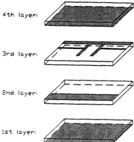
A packaged multilayer HTS filter composed of four YBCO films in a copper housing was designed. The dimensions of the package inner space were 30£ 16 £ 7 mm3. Three conductor layers were stacked on the bottom surface and one layer was attached to the top surface of the package space. The thickness of the conductor layer was 0.5 mm. The schematic representation of the layered structure is shown in Figure 1. The first conductor is used as the bottom ground, the second one is as a capacitor ground, the third one contains resonator patterns, and the fourth one is as the top ground. The detailed filter pattern, on the second and third conductor layers,
268 ° 2000 THE PHYSICAL SOCIETYc
is described in Figure 2. The dashed rectangle was the capacitor ground plane on the second layers. On the third layer, the 6 mm long and 0.2 mm wide of input/output microstripe lines were perpendicularly connected to the two resonator patterns (0.3 mm in width), respectively. The top ends of the resonators were respectively connected to a big rectangular pattern (1:0£ 1:9 mm2) having one end connected to the ground. The length of the resonators was 9.6 mm, and the distance between the two resonator patterns was 3.2 mm. In the vertical direction, there is a 5 mm air gap between the third and the fourth conductor layers for frequency response tuning. The filter was simulated by using 2D and 3D simulators contained in the software LINMIC+/N (by JANSEN MICROWAVE GmbH, GERMANY). The designed filter was a two-stage Tchebyscheff bandpass with the center of frequency (f0) at 1.9 GHz and band width (BW) of 50 MHz. Figure 3 shows the frequency response of a 2D simulation of the filter.
Commercial YBCO films deposited on 0.5 mm thick LaAlO3 substrates (" = 24) were used in this experiment. The specifications of the films are Tc > 87 K, Jc » 2 £ 106 A/cm2 at
77 K, and Rs · 0.6 m- at 10 GHz and 77 K (from THEVA GmbH, GERMANY). Loss tangent (tan±) of LaAlO3 was reported to be smaller than 10¡ 5 at 6.3 GHz and 77 K [5]. The usual photolithographic technique with wet etching method was employed to pattern the YBCO films. A surface profilometer was used to measure a post-etching strip with designed width of 300¹ m.
The width was determined to be 295¹m and the thickness was about 0.83 ¹m. Four YBCO films
were stacked in a copper housing to form a multilayer HTS filter. Two SMA connectors were attached to the copper housing as the input/output terminals. Ag paint was used to connect the SMA pins and the input/output of the filter patterns. Figure 4 shows the photo of the completed multilayer HTS filter.
FIG. 1. The scheme of four YBCO films stacked to form a HTS multilayer filter.
FIG. 2. The detailed filter patterns on conduct-ing layer 2 (dashed lines) and layer 3 (solid lines).
FIG. 3. Frequency response of a 2D simulation for a two-stage bandpass filter.
FIG. 4. Prototype of complete packaged multi-layer HTS filters.
A WILTRON 360B vector network analyzer (VNA) was used to measure the (reverse) reflection coefficient (S22) S11, and (reverse) transmission coefficient (S12) S21. A pair of low temperature coaxial cables(+150±C to -269±C) were connected to the input/output ends of VNA with each individual end, and the other ends were respectively connected to the SMA connectors of the packaged HTS filter. The filter with connected cables was then immersed into liquid nitrogen (77 K) to do measurements.
III. Results and discussion
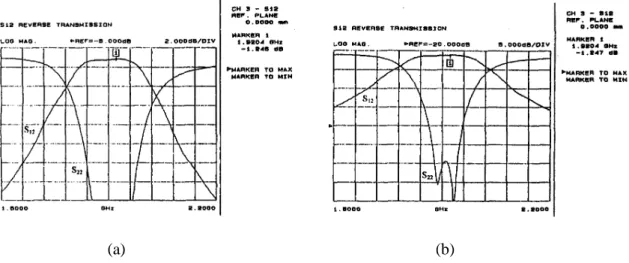
Figure 5 represents the first measurement of frequency response of the packaged multilayer HTS filter. The center of frequency was at 1.924 GHz, the band width was 150 MHz, and the minimum insertion loss (IL) was 2.564 dB at 1.996 GHz. It was found that there was a hump at » 2.7 GHz. From computer 3D simulation, we realized that it was due to the big transversal package spacing (perpendicular to the input/output terminals). The hump can be removed, if the transversal spacing is reduced in its length (e.g. from 16 mm reduced to 13 mm). The HTS filter was then rectified, by resembling the stacked YBCO films and reconnecting the joint points of the SMA pins and the input/output of the filter patterns. The rectified multilayer HTS filter was also measured at 77 K. Figure 6(a) represents the frequency response from 1.6 to 2.2 GHz. The center of frequency was at 1.91 GHz and the insertion loss (IL) was 1.246 dB (determined from S12). The reverse reflection coefficient S22 was determined to be» -40 dB and the band width was» 50 MHz (determined from the distance of the two S22 peaks), shown in Figure 6(b).
FIG. 5. The first measurement of frequency response of the packaged multilayer HTS filter.
(a) (b)
FIG. 6. Frequency response of the rectified multilayer HTS filter, with f0 = 1:91 GHz and IL = 1.246
dB (a) S22» -40.0 dB and BW » 50 MHz (b).
Comparing the insertion loss of this multilayer HTS filter to the previous reported papers [3; 4], we found that it had» 0.9 dB higher than those of them. It may be due to the high contact
resistance of Ag paint used at the joint points of SMA pins and the filter patterns. From the energy conservation, the signal energy loss can be determined by the following relation :
jS12j2+jS22j2+ Dissipated Energy = 1:
We estimated that the energy dissipation rate was about 0.25. It implied that 25% of signal energy was lost between the two SMA connectors.
VI. Conclusion
A multilayer HTS bandpass filter has been designed and fabricated. Four YBCO thin films deposited on LaAlO3substrates were stacked and placed into a copper housing to form a packaged multilayer HTS filter. The center of frequency was determined at 1.91 GHz with the band width of » 50 MHz. The insertion loss was 1.246 dB. It was estimated that about 25% of signal energy was lost. Most of energy loss may be due to the use of Ag paint at the joint points of SMA pins and filter patterns.
Acknowledgement
The authors would like to thank the Industrial Technology Research Institute of the Republic of China for financial support, and the National Research Council of the Republic of China under grant number NSC 87-2811-M002-0029.
References
[ 1 ] M. J. Scharen et al., IEEE Trans. on Appl. Supercond., 3744 (1997). [ 2 ] Gordon Roesler, MICROWAVES & RF, 61 (June 1998).
[ 3 ] G. L. Matthaei et al., IEEE MTT-S Digest, 457 (1996).
[ 4 ] A. Enokihara, and K. Setsune, J. of Superconductivity, Vol. 10, No. 1, 49 (1997). [ 5 ] C. Zuccaro et al., J. Appl. Phys. Vol. 82, No. 11, 5698 (1997).