國
立
交
通
大
學
物理研究所
博
博
博
博
士
士
士
士
論
論
論
論
文
文
文
文
兩個介觀物理的主題:
壹:低溫電子散射時間
貳:量子點中自旋傳輸
Two topics on mesoscopic electron transport:
Part Ⅰ:Low temperature electron dephasing time
Part
Ⅱ:Spin transport in vertical double quantum dots
研 究 生:黃旭明
兩個介觀物理的主題:
壹:低溫電子散射時間
貳:量子點中自旋傳輸
Two topics on mesoscopic electron transport:
Part Ⅰ:Low temperature electron dephasing time
Part
Ⅱ:Spin transport in vertical double quantum dots
研 究 生:黃旭明 Student:Shiu-Ming Huang
指導教授:林志忠 Advisor:Juhn-Jong Lin
國 立 交 通 大 學
物 理 研 究 所
博 士 論 文
A ThesisSubmitted to Institute of Physics College of Science National Chiao Tung University in Partial Fulfillment of the Requirements
for the Degree of Doctor
in Physics July 2008
A Thesis Done Under
NCTU-RIKEN Joint Graduate School Program
Student:Shiu-Ming Huang
NCTU Advisor:Juhn-Jong Lin
RIKEN Advisor:Kimitoshi Kono
Keiji Ono
兩個介觀物理的主題:
壹:低溫電子散射時間
貳:量子點中自旋傳輸
學生:
黃旭明指導教授
:林志忠 教授國立交通大學物理研究所 博士班
摘
要
在這本博士論文中,我們將討論兩個介觀物理的
主題。第一個是銅鍺金合金薄膜在低溫下電子的非彈
性散射時間的研究、第二個是電子在砷化鎵垂直雙量
子點中自旋傳輸的研究。
電子非彈性散射時間是一個度量電子處在其基
態時間長短的物理量。根據費米液體理論
(Fermi-liquid theory)的預測,電子在絕對零度
時,電子的非彈性散射時間會是無窮長。然而,多年
來眾多的實驗結果顯示,當溫度低於某個溫度後,電
子的非彈性散射時間會呈現一個不隨溫度改變的定
值。這個奇異的現象吸引了許多理論和實驗學家的注
意。有些理論學家認為不同於費米液體理論的預測,
這個現象是一個新的本徵物理性質。一開始在這
這個現象。經過長時間的研究,大部分的人都相信樣
品中磁性雜質的存在將會導致一個不隨溫度變動的
散射率,這等效於實驗上常常被觀測到的不隨溫度變
動的非彈性散射時間。在此之後,大不分的人都會將
觀測到奇異的非彈性散射時間歸因為近藤效應
(Kondo effect)
。我們也做了一些銅鍺金合金
(Cu
93Ge
4Au
3)薄膜的電子非彈性散射時間研究。我們
的結果顯示了三個非常特異的現象:第一、對於不規
則程度不同的樣品中,所有的樣品都在10度(10
K)跟6度(6K)之間呈現一個不隨溫度變動的非
彈性散射時間,而且對於所有的樣品在這區間非彈性
散射時間都是相同的。第二、當溫度低於6度(6K)
時,非彈性散射時間急速的增加而且增加的速率跟樣
品的不規則程度有關。對於一個不規則程度較高的樣
品,非彈性散射時間增加的速率比較快。第三、在1
0度(10K)到30毫度(30mK)區間,外加
高達15T的磁場依舊對電阻全無影響。所有的證據
顯示動態結構缺陷效應(dynamic structure defeat
effect)主宰整個系統行為。我們的結果是第一個有
系統分析這個效應的研究。
這幾年,因為在量子資訊上潛在的應用,量子點
中電子自旋的傳輸吸引了非常多研究上的注意。我們
也做了兩個垂直量子點的題目。
第一個是有關於自旋選擇法則。我們量測了銦鎵
偏壓法(large source-drain voltage),從雙電子
到三電子傳輸基態跟激發態的頻譜同時可以被觀測
到。在觀測到的頻譜中,從1S
2單重態到1S2P
三重態的基態過渡在5T被觀測到。在高於5T的磁
場下,可以清楚的看到黎蔓分離(Zeeman
splitting)
,而g值(g factor)是0.36。藉由
自旋選擇法則我們可以解釋在從雙電子到三電子的
傳輸中只有兩條黎蔓分離線而不是三條黎蔓分離
線.對於躍遷前後的電子自旋數大於1/2是不被允
許的。因為電子在自旋雙態(doublet state)的遲
逾時間(relaxation time)遠大於電子穿隧傳輸的
時間,所以上自旋(spin up)跟下自旋(spin down)
都可以成為傳輸的起始態。總共會有四個可能的傳輸
貢獻,但只有兩個有效能量可以在傳輸頻譜上被觀測
到。
第二個主題是有關於在黎蔓非吻合的量子點中
的自旋傳輸。我們量測了在不同g值的雙量子點的穿
隧電流(tunneling currents)
。結果是完全的不同
於相同g值的雙量子點的穿隧電流。特別的,因為兩
個電子點間黎蔓不吻合的穿遂,人們預測兩個分裂的
電流峰將會被觀測到。另外,聲子(phonon)的散射
強烈地影響到傳隧的電流值。在弱的聲子散射只有上
自旋電子可以共振(resonance)地穿遂,而下自旋
電子則不行。除此之外,帶寬(bandwidth)共振穿
Abstract
We report two mesoscopic topics in the thesis. First one is about the low temperature dephasing time in Cu93Ge4Au3 thin films and second
one is about the spin transport in InxGa1−xAs (GaAs) vertical double
quantum dots.
The electron dephasing time is a time scale that how long an electron can stay at its eigenstate. Fermi-liquid theory predicts that the life-time of an electron at the Fermi surface at T = 0 is infinite. However, many experiments show that the dephasing times are always constant at low temperature. The anomalous low temperature desphasing time catches many theorists’ and experimentalists’ interest. Some theorists propose that the saturating low temperature dephasing time is intrin-sic phyintrin-sics which is contrast to the Fermi-liquid theory. It makes a lot of controversy on the phenomenon. Many works were done to clarify the physics. After a lot of studies on the field, people be-lieve that magnetic impurities would induce a constant scattering time which is equal to the observed saturating dephasing time. After that, people often refer the anomalous low temperature dephasing time to the Kondo effect. We study the low temperature dephasing time in Cu93Ge4Au3 thin films. There are three distinct features. First one is
that the dephasing time is a constant value between 10 K and 6 K for all of measured films with different levels of disorder. Second one is that the dephasing time increases drastically as temperature is lower than 6 K. The increasing rates depend on the levels of disorder. For a more disordered film, the increasing rate is more drastic. Third one is that the temperature dependent resistance from 10 K down to 30 mK is insensitive to the magnetic filed up to 15 T. All of the results
support that the dynamic structure defeat effect dominates the be-haviors. Our experiment is the first systematic study on the dynamic structure defeat effect.
The electron spin transports in quantum dots have caught consider-able increasing of interest because of potential development on quan-tum information. We have done two subjects on spin transport in vertical double quantum dots.
First subject is about the spin-selection rule. We measured electron transport state spectra of an In0.05Ga0.95As vertical double quantum
dot. Both the ground and excited states of transport spectra from two electrons to three electrons are measured using a large source-drain voltage. In the obtained transition spectrum, the ground state tran-sition from the 1S2 singlet state to the 1S2P triplet state is observed
at 5 T. Zeeman splitting with a g-factor of 0.36 is clearly observed at magnetic fields higher than 5 T. The observation of two Zeeman sublevels instead of three for the triplet state is explained by the spin selection rules for the SZ components between the two-electron and
three-electron spin states. Transition with the total spin difference between the initial and final states larger than 1/2 is forbidden. Be-cause the relaxation time between doublet states is much longer than electron tunneling time, both spin up and spin down can be the initial states from spin transitions. There are four transitions contributing to tunneling processes, but only two energy differences lead to the two Zeeman sublevels in the excitation spectra.
The second subject is related to spin transport in Zeeman mismatch double quantum dots. We measure tunneling currents in a vertical double quantum dot with different g factors for the two dots. The results are substantially different from those in a double quantum dot with a homogeneous g factor. In particular, two split peaks are expected to be observed due to the Zeeman mismatch of inter-dot tunneling. In contrast to the case of a homogeneous g factor, the cou-pling to phonons strongly affects the tunneling current in the system
with an inhomogeneous g factor. For weak coupling strengths, only up-spin electrons can resonantly tunnel through the dots while the down-spin tunneling is spin blockaded. Besides, a bandwidth reso-nance tunneling peak also appears in the system with mismatched g factors.
Acknowledgements
First, I would like to thank Prof. Dr. Juhn-Jong Lin who guides me into the field of low temperature mesoscopic transport and study so many interesting topics together.
Second, I would like to thank Prof. Dr. kimitoshi Kono who gives me a chance to do research in his laboratory under the NCTU-RIKEN
Joint Graduate School Program and supports me living allowance and
research cost in Japan for three years.
Third, I would like to thank Dr. Hikota Akimoto who teaches me a lot of low temperature experimental technique. I would like to thank Dr. Keiji Ono who guides me into the field of quantum dot.
I also would like to thank people who ever help me in somewhere and someway.
Last but not least, I would like to thank my families who always give me a wide freedom to do what I decide.
Contents
1 Introduction 1
Part1: Low Temperature Electron Dephasing Time 2
2 Introduction to Low Temperature Dephasing Time 3
3 Theory and Background 9
3.1 Weak Localization . . . 9
3.2 Phase Breaking Mechanics . . . 12
3.2.1 Magnetic Field . . . 13
3.2.2 Spin-Orbit Scattering . . . 14
3.2.3 Spin-Spin Scattering . . . 16
3.3 Correction to Conductivity . . . 16
3.3.1 Localization: Two Dimensions . . . 17
3.3.2 Electron-Electron Interactions: Two Dimensions . . . 18
3.3.3 Kondo Effect . . . 19
3.3.4 Two-Level Systems . . . 22
4 Experimental and Technical Considerations 26 4.1 Introduction . . . 26 4.2 Sample Preparation . . . 26 4.2.1 Substrate Cleaning . . . 26 4.2.1.1 Metal Mask . . . 27 4.2.1.2 Photolithography . . . 27 4.2.2 Sputtering . . . 29
CONTENTS
4.3.1 4He Cryostat . . . . 35
4.3.2 3He Cryostat . . . . 37
4.3.3 Dilution Refrigerator . . . 37
4.3.4 Superconducting Magnet . . . 39
4.4 Measuring Circuit and Noise . . . 42
4.4.1 Measuring Circuit . . . 42
4.4.2 Johnson Noise . . . 42
4.4.3 Eddy Current . . . 44
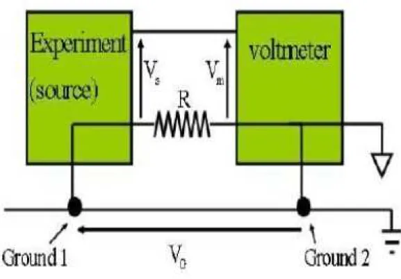
4.4.4 Ground Loop . . . 44
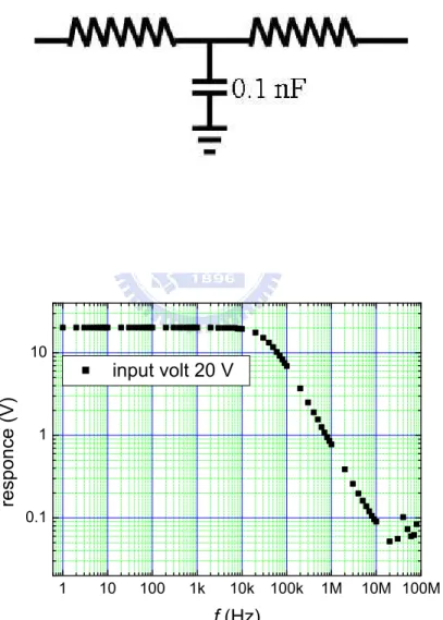
4.4.5 Filter . . . 45
5 Results and Discussions 49 5.1 Introduction . . . 49
5.2 Sample Background . . . 50
5.3 Magnetoresistance . . . 50
5.3.1 Electron-Electron Inelastic Scattering Time . . . 60
5.3.2 Electron-Phonon Inelastic Scattering Time . . . 63
5.3.3 Nagaoka-Suhl Theory and Numerical Renormalization Group 64 5.4 Low Temperature Resistance . . . 70
5.4.1 Kondo Effect . . . 71
5.4.2 Weak Localization . . . 75
5.5 Two-Level System . . . 77
Part2: Spin Transport in Vertical Double Quantum Dots 81 6 Introduction to Quantum Information and Quantum Dot 82 7 Theory and Background 85 7.1 Quantized Charge Tunneling . . . 85
7.2 Two Dimensional Electron Gas . . . 87
7.3 Two Dimensional Harmonic Oscillator . . . 88
7.4 Constant Interaction Model . . . 90
7.5 Low Source-Drain Voltage Region . . . 92
CONTENTS
7.7 Double Quantum Dots . . . 97
8 Experimental and Technical Considerations 105 8.1 Introduction . . . 105
8.2 Sample Fabrication . . . 106
8.3 Amplitude and Lineshape of Coulomb Oscillations . . . 106
8.4 Low Temperature Measurement . . . 109
8.4.1 Filter . . . 109
8.4.2 Shielding Room and Power . . . 111
9 Results and Discussions 114 9.1 Introduction . . . 114
9.2 Spin Selection Rule . . . 114
9.3 Spin Transport in Double Quantum Dots with Zeeman Mismatch 128
List of Figures
3.1 A conduction electron diffuses from point A to point B along
var-ious paths. . . 11
3.2 Electron diffuses in opposite directions of a loop and forms a con-struction at point O. . . 11
3.3 A electron diffuse in a d-dimensions space. . . 15
3.4 Schema of spin-orbit interaction. The initial spin state is S. After several scattering of spin-orbit coupling, two final states of two partial waves are S’ and S”. . . . 15
3.5 A schema of interaction between s electron and d electron. The s electron scatters from the (k, ↑) to (k0, ↑). . . . 21
3.6 A schema of two-level system. . . 24
3.7 Temperature dependence of two-level system in three different cases. 24 4.1 Processes of deposition by using metal mask. . . 28
4.2 Processes of deposition by using photolithography. . . 30
4.3 Principle of planar magnetron sputtering. . . 32
4.4 The picture of film which is fabricated by photolithography. . . . 33
4.5 The operating principle of 1K cryostat. . . 36
4.6 The operating principle of 3He cryostat. . . . 38
4.7 The operating principle of dilution refrigerator. . . 40
4.8 Operating principle of superconductor magnet. . . 41
4.9 The schema of measuring circuit. . . 43
4.10 The schema of ground loop noise. . . 46
LIST OF FIGURES
4.12 The schema of ferrite beat. . . 48
5.1 Spectrographic analysis . . . 51
5.2 Magnetoresistances of Cu 38-1 at several temperatures. . . 53
5.3 Dephasing time of Cu 38-1 as a function of temperature. . . 54
5.4 Dephasing time of Cu 38-1 as a function of temperature in double-logarithmic scales. . . 55
5.5 Magnetoresistances of Cu 18-2 at several temperatures. . . 57
5.6 Magnetoresistances of Cu 40-1 at several temperatures. . . 58
5.7 Magnetoresistances of Cu 43-1 at several temperatures. . . 59
5.8 Temperature dependence of dephasing times of all samples. All of the dephasing time are shifted 2 ps one by one, except sample 43-1 and sample 44-1. The respective sheet resistances of 9 K are shown in the insect. . . 61
5.9 Dephasing times at 0.4 K and 6 K. . . 62
5.10 Temperature dependence of dephasing times of yet-to-be identified. The dots are the measured data of sample 27-3 and the line is the prediction of NS theory. . . 67
5.11 Temperature dependence of dephasing times of yet-to-be identified. The dots are the measured data of sample 38-1 and the line is the prediction of NS theory. . . 68
5.12 Temperature dependent resistance of samples 18-4. . . 72
5.13 Resistances of four samples as a function of temperature. All of the dependence are logarithmic dependence. . . 73
5.14 Temperature dependent resistance of sample 44-1 at 0 T and 9 T. 74 5.15 Temperature dependent resistance of thick sample at 0 T, 5 T, 10 T, and 15 T. . . 76
7.1 Schema of a quantum dot. . . 86
7.2 Calculated single-particle energy as a function of magnetic fields for a parabolic potential with ~ω0 = 3 meV. . . 89
7.3 determine the α factor from the slope of the sides of the Coulomb diamond. . . 91
LIST OF FIGURES
7.4 Schematic diagrams of the electrochemical potential levels of a
quantum dot in the low-bias regime. . . 93
7.5 Schematic diagrams of the electrochemical potential levels of a quantum dot in the high-bias regime. . . 95
7.6 Schematic diagrams of the differential conductance as a function of source-drain voltage and gate voltage. . . 96
7.7 Network of tunnel resistors and capacitors representing two quan-tum dots coupled in series. . . 98
7.8 Schematic stability diagram of the double dot system for (a) small, (b) intermediate, and (c) large interdot coupling. The equilibrium charge on each dot in each domain is denoted by (N1, N2). The two kinds of triple points corresponding with the electron transfer process (•) and the hole transfer process (◦) are illustrated in (d). 101 7.9 Schematic stability diagram showing the Coulomb peak sapcings. 103 8.1 The processes for fabricating quantum dot. . . 107
8.2 The fabricated quantum dot and wirings. . . 108
8.3 The lineshape of Coulomb oscillation in quantum regime at differ-ent temperature. The parameter are ∆E = 0.01e2/C and k BT /∆E = 0.5, 1, 7.5, and 15 for line a, b, c, and d respectively. . . 110
8.4 The transection of filter. . . 112
8.5 The schema of the power in shielding room. . . 113
9.1 The structure of vertical double quantum dots. . . 116
9.2 Coulomb diamond. . . 118
9.3 The measured differential conductance as a function of gate voltage and magnetic fields. . . 119
9.4 The schematic diagram of tunneling through the dots. . . 120
9.5 The extracted Zeeman energy as a function of magnetic fields. . . 122
9.6 The schematic diagram of spin selection rule. . . 124
9.7 The differential conductance of GaAs as a function of source-drain voltage and gate voltage. . . 126
9.8 The extracted Zeeman energy of GaAs as a function of magnetic field. . . 127
LIST OF FIGURES
9.9 The structure of vertical double quantum dots with different g
factors. . . 129
9.10 The schema of the potential barrels of the dots. . . 130
9.11 Differential conductance, dIsd/dVsd, as a function of source-drain voltage and gate voltage. The arrows mark the resonance tunneling peaks of from ground state of left dots to different states of right dot. . . 132
9.12 Resonance tunneling and co-tunneling peaks. . . 133
9.13 The inter-dot tunneling peak of chose state. . . 135
9.14 The current through the system vs source-drain voltage consists of a series of peaks corresponding to photon-assisted tunneling line between two dots. . . 136
9.15 Splitting of tunneling peak due to Zeeman mismatch. . . 138
9.16 The respective Schematic figures of tunneling peak due to Zeeman mismatch. . . 139
9.17 The measured results of differential conductance at 13 T. . . 141
9.18 The measured results of differential conductance at 10 T. . . 142
9.19 The measured results of differential conductance at 9 T. . . 143
9.20 The measured results of differential conductance at 7 T. . . 144
9.21 The extracted Zeeman energy, δ1. . . 145
List of Tables
4.1 Sputtering parameters of Cu93Ge4Au3 films. . . 34
Chapter 1
Introduction
Low temperature mesoscopic transport is a very interesting topic in research no matter on the technique application or basic scientific study. The more we study, the more new and fantastic physics and phenomena are discovery and invented. In the thesis, I report two mesoscopic topics which I have studied in the years. The first one is concerning low temperature electron dephasing time in Cu93Ge4Au3 thin films and the second one is concerning the electron spin
transport in InxGa1−xAs (GaAs) vertical double quantum dots. I will discuss the
first one topic, low temperature dephasing time, in the part 1 from chapter 2 to chapter 5 and discuss the second topic, spin transport in dotble quantum dots, in the part 2 from chapter 6 to chapter 9. Last, I would give conclusions and future works in the chapter 10.
Part1:
Low Temperature Electron
Dephasing Time
Chapter 2
Introduction to Low
Temperature Dephasing Time
The motion of conduction electron in solids has long been a subject of interest and fascination. In a crystalline or ordered material, where the potential is periodic, the conduction electron are well described by Bloch theory which the electron wave function are specially extended throughout the system. The electrical con-duction in such a system can be described by the Boltzmann transport. The results of the theory are that at high temperatures the resistivity is dominated by phonon scattering and at low temperature the resistivity is dominated by the impurities. The Boltzmann equation predicts, in the low temperature regime, a resistivity which is given by
ρ(T ) = ρe+ AT5, (2.1)
where A is a constant, and ρe is the residual or impurity resistivity, which is
caused by collision of electron with impurities. Since the impurities are treated as static, the residual resistivity is temperature independent. It is also well known that in the formalism of Boltamann transport theory the impurity concentrations are assumed to be extremely low. In the extremely disordered limit, the scattered electrons can be described by superpositions of Bloch waves.
In 1958, Anderson(1) pointed out that,when the randomness or disorder in the potential is sufficient high, i.e., in the strong disorder limit, the electron wave
functions may be altered from the Bloch forms. He showed that the electron wave would be localized in regions where the potential is particularly suitable. Thouless(2; 3) and co-workers(4; 5) had tempted to formulate a scaling descrip-tion of the localizadescrip-tion problem. They predicted that in one dimensional system, once the residual resistance of a wire exceeded a critical value of the order of ~/e2
(∼ 4KΩ), hence the electronic states would be localized. Several experiments had been reported to check this prediction.
In 1979, Abrahams, Anderson, Licciardello, and Ramakrishnan(6) based on those arguments of Thouless and co-works(2; 3; 4), successfully constructed a scaling theory of localization. They concluded that, in the presence of any amount of impurities, there would be no extended states in two dimensional systems. They showed that the conductance would undergo a crossover from a logarithmic decrease to an exponential decrease with increasing the linear dimension of the system. In three dimensional system, the scaling theory predicted that the metal-insulator transition would be continuous.
The localization theory is a single particle description. Considering many body effects, Al’tshuler and Aronov(7; 8) pointed out that the interaction be-tween the conduction electrons, in the presence of weak disorder, would have strong effects on the transport properties. They studied the Coulomb inter-actions between screened, two dimensional electrons whose motion is diffusive. They found the interactions between electrons are greatly enhanced in this case, causing a logarithmic singularity in the density of states in turn results in a non-ohmic conductivity which is similar to that predicted by localization.(9;10) This theory is commonly referred to as electron-electron interaction theory. Such a singularity in the density of states led to very similar effects on the electronic transport properties as those predicted by the weak localization theory.
There have been a number of experimental studies in the past several years of various types of disordered conductors, which have been aimed at testing these predictions. The behavior of the resistance as a function of temperature agreed qualitatively with the theory. These experiments have also shown that the be-havior is strongly dependent on the system dimensionality.(11; 12;13; 14)
To differentiate between the weak localization effects and the electron-electron interaction effects, magnetoresistance measurements are extremely important.
Hikami, Larkin, and Nagaoka,(15) and Al’tshuler and co-worker(9; 10; 16) con-sidered the effects of a magnetic field on the behavior of resistivity at low tem-peratures. These studies showed that localization and interaction respond very differently to a magnetic field. It turns out that localization effects result in an anisotropic magnetoresistance in a very low magnetic field regime. Interaction ef-fects, on the contrary, result in an isotropic magnetoresistance, but the magnitude of this magnetoresistance is important only at significantly high magnetic fields. It was also found that the effects of spin-orbit scattering and spin-spin scattering can be very important. If the spin-orbit scattering is strong enough, it can cause an effect with a sign opposite to that of localization.(17) That is, it cause the resis-tance to decrease as the temperature is lowered, rather than increase. This effect is known as anti-localization. A number of very successful measurements have been performed to test these predictions.(17; 18; 19;20;21;22;23) In particular, magnetoresistance measurements have been used to infer the electron inelastic scattering time, the spin-obit scattering time, and the spin-spin scattering time, and hence the overall contribution to the zero field behavior from localization an be determined.
It is well established that one can extract the electron-phonon scattering time, electron-electron scattering time, spin-orbit scattering time, and spin-spin scattering time from magnetoresistivity measurements. There have been many experiments done in this direction to obtain these phase breaking times which have proved that this is a very reliable method. There have been many experi-ments using this method to obtain the phase breaking times in different dimen-sional systems. Bergmann does a lot of works on spin-orbit inelastic scattering time.(24;25;26) Lin and Giordano(27;28) study the electron-electron scattering time in 1D and 2D in AuPd films. Their results are good agreement with theoreti-cal predictions and widely accepted. In experimental side, Lin and Wu(29;30;31) and many scientists study the electron-phonon inelastic scattering time, τep, in
many different systems(32; 33; 34; 35). They point out that the τep ∝ T−p where p ranges from 2 to 4. In theoretic side, Sergeev and Mitin establish a phonon-drag
theory which can explain experiment results well.(36; 37; 38)
Lin and Giordano perform systematic measurements of inelastic scattering times in several AuPd films. They point out the the saturated inelastic times
depend on the sheet resistance, R¤, and conclude that the observed saturation
inelastic scattering time cannot be explained in terms of magnetic scattering. Af-ter that, more and more experimental works observe the same behaviors. In 1997 Mohanty(39) collects many experimental results and points out that experiment always observe a constant τφ when temperature is sufficiently low. The
satu-ration of τφ occurs in both one and two dimensional metal and semiconductor
mesoscopic structures. The observation of τφ saturation immediately triggered
many experimental and theoretical groups asking whether the saturation might be universal in all material systems and dimensions.
The electron dephasing time τφ is one of the most important quantities
gov-erning quantum interference phenomena. Recently, the behavior of the dephasing time near zero temperature, τ0
φ has attracted many experimental(39; 40; 41; 42; 43; 44; 45; 46; 47) and theoretical(48; 49; 50; 51; 52; 53; 54; 55; 56) attentions. One of the central themes of this renewed interest is concerned with whether τ0
φ
should reach a finite or an infinite value as temperature approach 0 K. The con-nection of the τ0
φ behavior with fundamental condensed matter physic problems,
such as the validity of the Fermi-liquid picture, has been intensively addressed. Conventionally, it is accepted that τ0
φshould reach an infinite value in the presence
of only electron-electron and electron-phonon scattering. For a long time, the saturation behavior of τ0
φ has often been ascribe to a finite
spin-spin scattering time, due to the presence of a tiny amount of magnetic im-purity in the sample. Such a finite scattering rate will eventually dominate over the relevant inelastic scattering in the limit of sufficiently low temperatures. The idea of magnetic scattering induced dephasing immediately became widely ac-cepted. Hikami greatly shaped the current understanding of the effect of spin-flip scattering on the weak localization magnetoresistance. According to the descrip-tion, magnetic scattering can lead to decoherence between the two time-reversed wave traversing a closed loop, resulting in a suppression of weak localization and related quantum interference effects. Generally, the spin-spin scattering time is taken to be essentially independent of temperature, compared with the relatively strongly temperature-dependent electron-phonon and electron-electron scatter-ing times. With this Understandscatter-ing, it is natural to interpret any saturated τ0
φ
The Saclay-MSU group has measured the dephasing time of quasiparticles in several noble metal narrow wires. They found that the τφ varies as T−2/3
which is the prediction of one dimension Nyquist electron electron scattering time down to 40 mK. Once, several ppm magnetic impurities are doped into the wires, measured inelastic scattering times show a weak temperature dependent at low temperature. They concluded that a saturation of τφ occurs only in wires
that contain a small amount of magnetic impurity.(57; 58)
In contrast to the conclusion reached by the Saclay-MSU group discussed above, Mohanty et. al.,(45;59) have tested and argued for a non-magnetic origin for the saturation behavior of τ0
φ. Mohanty et. al., first study very pure Au
wires (containing less than 1 ppm of magnetic impurities), finding that there is always a saturation of τ0
φ. From these measurements, they find realizes that
both the values of τ0
φ and the onset temperature of saturation could be tune by
adjusting the sample parameters such as the wire length, resistance, and diffusion constant. To explore this idea, Webb et. al., repost further measurements on several carefully fabricated Au wires, whose onset temperature of saturation is indeed push down to very low temperatures. Webb et. al., argue that τ0
φ should
still saturate in these wires at a temperature ¿ 40 mK.
To clarify the effect of magnetic scattering on τφ, Webb et. al., ion implant
several ppm of Fe impurities in their pure Au wires. They find that τφ decreases
by more than an order of magnitude upon adding these impurities, but remains temperature dependent down to 40 mK. Therefore, they concludes that the sat-uration behavior of τ0
φ observed in pure Au wires can not be due to magnetic
scattering. In addition, they point out that saturation behavior of τ0
φ is also
of-ten observed in semiconductor mesoscopic structures. Since such structures are thought to contain only the smallest concentration of magnetic impurities, they conclude that the widely observed saturation must be universal and can not be simply due to magnetic scattering. It should be noted that the sample properties of the Au wires studied by Webb and co-workers were essentially similar to those studied by Saclay-MSU group.
Beside of the scattering forms discussed above, dynamic structure defeat is another source of saturation of τ0
φ.(60;61; 62;63;64;65;66; 67;68) The simplest
doublet well potential, the two wells being localized along a line directed between their centers which are separated by a displacement. In the absence of coupling to a bath of excitations, the lowest two states of the atom are, approximately, the positional eigenstates associated with harmonic oscillations within either well. The next level usually has energy above the barrier between the well minima and therefore is not localized to either well. Atoms may move between the two positions on quantum-mechanic tunneling. In the process, the atom directly tunnels through the potential barrier between the wells. Because of the thermal activated transitions, this process must dominate at sufficiently low temperatures. The original motivation for studying such a model was the observation of log-arithmic anomalies in the resistivity of metallic glasses.(11;69) Most of the works also only focused on the resistivity, specific heat, and susceptibilty. Only a few works on electron dephasing time are reported. Lin and co-workers study the annealing effects in a lot of three-dimensional polycrystalline disordered metal films.(70) They perform systematic measurements of τϕ on several series of
sput-tered and subsequently annealed AuPd and Sb thick films. Such controlled an-nealing measurements are crucial for testing theoretical models of dephasing that invoke the role of magnetic scattering and dynamical defeats.
In the first part of the thesis, I will discuss our experimental observation of temperature dependence of dephasing time in Cu93Ge4Au3films. Our results
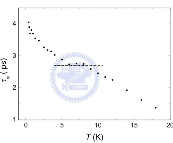
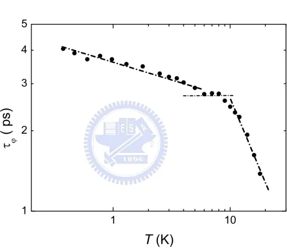
indi-cate that a very short electron dephasing time possessing very weak temperature dependence around 6 K, followed by an upturn with further decrease in temper-ature below 4 K. The low tempertemper-ature upturn is progressively more pronounced in more disordered samples. Resistance is logarithmic increase with decreasing temperature in wide temperature range and it is insensitive to magnetic field up to 15 T. In the thesis, we will discuss the temperature dependent resistance at different magnetic field and temperature dependent dephasing time in series of samples with different levels of disorder on weak localization effect, Kondo effect, and two-level system effect. Synthesizing all discussion, we can rule out all others inelastic scattering and make sure out observed low temperature dephasing time is from two-level system scattering. This is the first systematic work discussing the disorder dependence with low temperature temperature dephasing times of dynamic structure defeat effect.
Chapter 3
Theory and Background
3.1
Weak Localization
The usual Boltzmann transport theory is based on that, between two collision events, the electrons move along classical trajectories. Every scattering and two trajectories are treated as independent. For this classical transport theory to be valid, the scattering centers much be independent of each other. Therefore, the theory is valid only when the elastic mean free path, le is much larger than the
electron Fermi wavelength λF. On the other hand, if the condition is no longer
satisfied and le ∼ λF the electron eigenstates might become localized. This
phenomenon was first proposed by Anderson.(1) After this proposition, everyone believes that the electron states are localized states in strong disordered systems and electron states are extended states in good latticed systems. Concerning a system that the condition, le > λF is still holds, but the scattering can no longer
be treated as independent. The electron wavefunctions interference can not be neglected any more and this interference causes the electron states to be weakly localized.
The electron motion in weak disordered systems is diffusive rather than bal-listic or hopping. Here we assume that the time of all inelastic scattering are much longer than the elastic collision time and the electron wavelength is much short than the mean free path. Under these assumptions, electrons can be treated wave packets. As shown in Fig. 3.1, an electron diffuses from point A to point B along different paths 1, 2, 3. The form of the individual path reflects the nature
3.1 Weak Localization
of diffusive motion of electrons in a system with impurities. According to general principles of quantum mechanics, the total probability, P , of reaching point B from point A is P = ¯ ¯ ¯ ¯ ¯ X i Ai ¯ ¯ ¯ ¯ ¯ 2 =X i |Ai|2+ X ij AiA∗j, (3.1)
where Ai is the probability amplitude of path i. In the first part from right
hand side of Eq. 3.1, the first term is the sum of the probabilities corresponding to separate trajectories and is also the probabilities corresponding to classical diffusion. The second term is the interference terms that different wave pockets interfere along the trajectories. In the classical transport, the interfering term is not important and contributes nothing to the conductivity.
However, there is an exception, when point A and point B coincide, the elec-trons have two different ways to propagate around the loop, either clockwise or counterclockwise. As shown in Fig. 3.2 one partial wave goes in the direction of 0 → 1 → 2 → 3 → 4 → 5 → 0, and the other partial wave goes in the opposite direction 0 → 5 → 4 → 3 → 2 → 1 → 0. If all the propagating processes along the loop are elastic scattering, the phases of two partial waves are in phase at point O, and the interference term is full constructed. As a result, the probability of finding the electron at point O is enhanced, twice higher than the case of out of phase. In other words, quantum particles are less mobile in a random potential than that would be expected from Boltzmann transport theory. The enhanced ”localized” probability contributes a decrease in conductivity or, equivalently an increase in resistance. This is the well known weak localization.
Instead of calculating the quantum corrections to the conductivity following diagrammatic techniques and the Kubo formula, we estimate the corrections by probability arguments. We consider an electron diffuses in a random potential and describe its motion using diffusion equation. At time t, the probability of an electron staying at the position r is
P (r, t) = 1
(4πDt)d/2e
−r2/4dt
3.1 Weak Localization
Figure 3.1: A conduction electron diffuses from point A to point B along various paths.
Figure 3.2: Electron diffuses in opposite directions of a loop and forms a con-struction at point O.
3.2 Phase Breaking Mechanics
where D is the diffusion constant and d is the system dimensionality. The prob-ability of electron localized in origin point is
P (0, t) = 1
(4πDt)d/2. (3.3)
Considering a condition that a electron diffuses in a path, as shown in Fig. 3.3. The electron travels a length vFdt during a time interval dt and cross section is
(~/mvF)d−1 in d dimensions space. The corrections to the conductivity, ∆σ/σ,
are proportional to the ratio of the back-scattering volume to the total diffusion volume. so the magnitudes of the quantum corrections to the conductivity are given by ∆σ σ ∼ − Z τφ τe vF × (mv~F)d−1 (Dt)d/2 dt = − Z τφ τe λd−1 F vF (Dt)d/2dt, (3.4)
where τe is the elastic scattering time and τφis the phase-relaxation time. The τφ
means that how long the electron stays at its eigenstate and keeps the electron wave phase coherence. The negative sign in Eq. 3.4indicates that the conductiv-ity is reduced from the Boltzmann conductivconductiv-ity. It comes from the interference of two partial wave as shown in the interference term of the Eq. 3.1. Integrating Eq. 3.4, one can get that
∆σ ∼ −e 2 ~Lφ, for d = 1, ∆σ ∼ −e2 ~ln( Lφ le ), for d = 2, (3.5) ∆σ ∼ −e2 ~ 1 Lφ , for d = 3,
where Lφ is the phase-coherence length which is defined by Lφ = (Dτφ)1/2.
3.2
Phase Breaking Mechanics
From the above discussion, it is clear that the quantum corrections to conductivity are very sensitive to the phase of the electron wave. There are several kinds of electron scattering can destroy the phase coherence of the wavefunction. Next, we will discuss them respectively.
3.2 Phase Breaking Mechanics
3.2.1
Magnetic Field
It is well known that in quantum mechanics the hamiltonian for a charged particle in a magnetic field is obtained by replacing the momentum operator ~p by ~p − e ~A,
where ~A is the vector potential, and hence that the basic effect of a magnetic
field is to introduce an extra factor ∆Φ = −e
~ I
~
A(~r, t) · d~r, (3.6)
to phase of the corresponding wave function.
If a magnetic field is applied perpendicular to the closed loop, both of the partial waves will acquire an extra phase of the same magnitude, but with opposite sign because the directions of the integration path are opposite. Therefore the coherence interference of the electron waves is diminished and the corrections to conductivity is reduced. Assuming the ~A is time independent, the relative change
of the phase of the two partial waves is two times larger than that in Eq. 3.6
∆Φ = −2e ~ I ~ A · d~r = 2e ~Φ, (3.7)
where the integration is along the closed loop traveled by the two partial waves and the Φ is the magnetic flux penetrating the closed loop area. If the phase difference ∆Φ ∼ π, the weak localization effect is entirely suppressed
π = 2e
~ H × (closed loop area). (3.8)
For a diffusive electron, the closed loop area is order of Dτi where D is the
diffusion constant and τi is inelastic scattering time. We get that localization
effect will be entirely suppressed at a magnetic field of order
Hc≈
~
eDτi
, (3.9)
which is of order of 1kG in real cases. Here Hc is referred to as the ”critical
magnetic field.” It is important to note that the destroy phase coherence leads to a negative magnetoresistance with increasing magnetic field.
3.2 Phase Breaking Mechanics
3.2.2
Spin-Orbit Scattering
A moving charge in a lattice will feel an effective magnetic field
~
Bef f = −
~v
c × ~E, (3.10)
where ~v is velocity of the moving charge, c is the speed of light, and ~E is the
electric field comes from nucleus electric charges. A simple picture explaining the spin-orbit scattering effects on weak localization is introduced by Bergmann.(17) For each spin-orbit scattering, a electron spin rotates a small angle. Because the rotation operator does not commute, the two final spin states of the two partial waves are not the same. Therefore, the constructive interference of the two partial wave is destroyed. To consider two partial waves in spin-state ~S,
we present spin operator ~R. As shown in Fig. 3.4, the operator rotates one of the initial spin state ~S to final spin state, ~S0. ~S0 = ~R · ~S. The operator is
described by Eulerian angle. In the opposite direction, the final spin state is
~
S00 = ~R−1· ~S. The spin states of the two partial waves are different. The scalar
product is < ~S0| ~S00 >=< ~S|R2|~S >, so the two partial waves are coherence only
when R2 = 1. The coherence condition corresponds to the spin-orbit scattering
time τso being very large as compared with the inelastic scattering time τi. If the
condition is not satisfied, then the spin-orbit scattering will suppress the coherent back-scattering and lead to increase of the conductivity.
In the strong spin-orbit coupling limit, Bergmann has shown that phase differ-ence between two partial waves is most equal to 2π. However, this is a destructive interference because the spin electron has a rotational periodicity of 4π. This phe-nomenon of decreased resistivity in the presence of strong spin-orbit scattering is called weak anti-localization.
Stephan and Bergmann(71) have suggested that the spin-orbit scattering cross section should also depend on the total orbital angular momentum L and total spin angular momentum S. They predicted that the spin-orbit scattering cross section is σso= 4π EF X l l(l + 1) 2l + 1 sin 2[δso l+1/2,l(EF) − δl−1/2,lso (EF)], (3.11)
3.2 Phase Breaking Mechanics
Figure 3.3: A electron diffuse in a d-dimensions space.
Figure 3.4: Schema of spin-orbit interaction. The initial spin state is S. After several scattering of spin-orbit coupling, two final states of two partial waves are
3.3 Correction to Conductivity
where EF is the Fermi energy of the host, δso is the phase shift contributed
by spin-orbit scattering which depends both on the total angular momentum,
j = l ± 1/2 and angular momentum, l.
3.2.3
Spin-Spin Scattering
The presence of localized spins or magnetic impurities introduces a pertubation part in the Heisenberg coupling
Hs= J ~S1· ~S2, (3.12)
where J is an exchange constant and ~S1 and ~S2 mean the spins of electron and
ion spins respectively. This perturbation destroys the time-reversal symmetry of the hamiltonian. The localized moment breaks the coherence of the two partial waves. It is noticeable that the influence on the weak localization is similar to that of the inelastic scattering on the weak localization. The spin-spin scattering time can be expressed as
1
τs
∼ 2πN(EF)niJ2S2, (3.13)
where N(EF) is the density of state at the Fermi energy and ni is the density of
the magnetic impurities.(72)
3.3
Correction to Conductivity
It is well known that both localization and electron-electron interaction play fun-damental roles in disordered systems. It is also clear that, especial since the work of Thouless, that the behavior is strongly dependent on the dimensionality. The first theoretical work predicted that the behavior would depend on the resistance (sheet resistance in two dimensions) and on the electron inelastic scattering time. Later works have shown that other types of scattering, namely the spin-orbit scattering and spin-spin scattering (magnetic impurity scattering), are also im-portant. Moreover, the theory makes explicit predictions for the behavior of the resistance as a function of both temperature and magnetic field. Next, I would like to discuss the corrections of several interactions to conductivity.
3.3 Correction to Conductivity
3.3.1
Localization: Two Dimensions
In two dimensions, it is convenient to consider the resistance per square, R¤
(also known as the sheet resistance), which is just the resistivity divided by the thickness d, R¤ = ρ/d. For a system in which spin-orbit scattering and spin-spin
scattering are negligible and in the absence of a magnetic field, localization makes a contribution to the sheet resistance which is of the form
∆R¤(T ) R¤(T0) = −αe 2p 2π2~R¤(T0)ln( T T0 ), (3.14)
where α is a constant which depends only on general symmetry and parameter
p is determined by the temperature dependence of the inelastic scattering time.
In generally, the αP is an integer of order unity. T0 is an arbitrary reference
temperature which is about 10 K in our experiments. In general case, when a magnetic field is present and other types of scattering cannot be neglected, it is considerably more complicated. It is found at a fixed temperature that
∆R¤(H) R2 ¤(0) = − e 2 2π2~{Ψ( 1 2+ H1 H) − Ψ( 1 2 + H2 H )} + e 2 4π2~{Ψ( 1 2 + H3 H ) − Ψ( 1 2+ H2 H )} − e 2 2π2~{ln( H1 H ) − 3 2ln( H2 H ) + 1 2ln( H3 H )}. (3.15)
where Ψ is the digamma function and the ”fields” H1, H2, and H3 are described
by H1 = He+ Hso+ Hs, H2 = Hi+ 4 3Hso+ 2 3Hs, (3.16) H3 = Hi+ 2Hs,
He, Hso, Hs, and Hi mean elastic, spin-orbit, spin-spin, and inelastic scattering
”magnetic field” respectively. Here the magnetic field, H, is assumed to be per-pendicular to the plane of the film. The respective ”magnetic field” connects to the corresponding scattering time by the formula
3.3 Correction to Conductivity
Hx =
~ 4eDτx
. (3.17)
Note that the He is generally much larger than any of the other fields in the
problem.
It is important to keep in mind several points concerning these predictions. First, a film will behavior two dimensionally only when its thickness is less than the phase breaking length, Lϕ = (Dτϕ)
1
2, where the phase-breaking time, τϕ, is
the time scale over which phase coherence is maintained. This condition on the film thickness provides a consistency check on the analysis. Also, the conventional or classical magnetoresistance which is of order
∆R(H)
R(0) ≈ (ωcτe)
2, (3.18)
Where ωc is the electronic cyclotron frequency, is generally much smaller than
that predicted in Eq. 3.15 in the low magnetic field regime of interest, so it can be ignored.
Finally, spin-orbit scattering plays a very important role, since it determines the sign of both the magnetoresistance and the change of the resistance in zero magnetic field. The magnetoresistance is negative and the zero field resistance change is positive for weak spin-orbit scattering. In the opposite case, the correc-tion to the resistance changes sign and is magnitude is reduced by a factor two. The later case is often referred to anti-localization.
3.3.2
Electron-Electron Interactions: Two Dimensions
It is well known that the behavior of the resistivity resulting from electron-electron interactions, in zero magnetic field, are very similar in form to that due to lo-calization. The theory of electron-electron interactions has been studied. In two dimensions, they found that the correction to conductivity, in the absence of a magnetic field, as a function of temperature is
∆R¤(T ) R¤(T0) = − e 2 2π2~ (1 −3 4F )R¤ln( T T0 ), (3.19)
3.3 Correction to Conductivity
where F is a screening factor. In a well screened system, F approaches unity and in the opposite limit, F approaches zero.
In the presence of a magnetic field, the interaction theory predicts an positive, isotropic magnetoresistance. However, since this prediction is concerned with the splitting of the electron spins energy bands, it is not noticeable at low magnetic fields. Therefore, this effect will not be considered in this thesis.
3.3.3
Kondo Effect
Since first experimental observation of increasing resistivity with decreasing tem-perature in gold, the resistance minimum was a long standing theoretical puzzle. The later observation, that the minimum depended on the impurity concentra-tion, indicated it as being an impurity phenomenon. Kodon observed a correlation between the existence of Curie-Weiss term in the impurity susceptibility (a local moment) and the occurrence of the resistance minimum. Kondo calculated the conductivity to higher terms of s − d model and his results can well explain the experimental observation.
In some cases, the impurity atom may retain its magnetic moment in a metal. An isolated atom generally has a spin and orbital angular momentum according to Hund’s rule. For a transition metal ion, one that displays evidence of local moment behavior as an impurity in a metal, it might be reasonable to describe it as in an insulator and then consider the effects of the ion magnetic moment on the conduction electrons. Zener proposed a model of ferromagnetic transition metals in which it is assumed that the d electrons are localized at the atomic sites and the s electron are itinerant over the entire crystal. He considered an exchange interaction between the two kinds of electrons,to which he attributed the ferromagnetism of the 3d metals. For a single impurity in a metal the interaction takes the form,
Hsd = X k,k0 Jk,k0(S+c† k,↓ck0,↑+ S−c † k,↑ck0,↓+ Sz(c † k,↑ck0,↑− c † k,↓ck0,↓)) (3.20)
where Sz and S±(= Sx ± iSy) are the spin operator for a state of spin S. It
3.3 Correction to Conductivity
conduction electrons with a coupling constant Jk,k0. c†k,σ and ck0,σ are creation
and annihilation operators for the conduction electrons. There are terms in this interaction in which the spin of the conduction electron is flipped on scattering with the impurity.
To calculate the resistivity to third order in J, the form becomes
< k0, σ0|T (²)|k, σ >=< k0, σ0|HsdG(²)Hsd|k, σ > (3.21)
where T is a matrix of that between states of Slater determinants in which a conduction electron is scattering from a state (k, σ) to a state (k0, σ). G(²) is
green function. There are many contributions to this matrix element, the most important terms are the ones in which the spins of the conduction and localized electron are flipped. The modification required in the calculation of the T matrix in the many body case can be stated quite simply; we have to replace the occu-pation numbers for electrons (holes) in the intermediate k states by Fermi factor
f (²k) (1 − f (²k)).
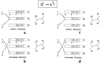
There are four possible processes: from < k, ↑ | to |k0, ↑>, from < k, ↑ | to
|k0, ↓>, from < k, ↓ | to |k0, ↑>, and from < k, ↓ | to |k0, ↓>. First, we consider
the first scattering process, from < k, ↑ | to |k0, ↑>. The contribution is
J2 N2 s X k1,k01,k2,k20 < k0, ↑ |S−c† k1,↑ck01,↓(² + is − H0) −1S+c† k2,↓ck20,↑|k, ↑> (3.22)
The form means that the (k, ↑) conduction electron scatters with spin flip in to an unoccupied hole state (k2, ↓). The (k2, ↓) electron then scatters into the final
(k0, ↑) state. Intermediate k lines running from left to right carry a hole factor
1 − f (²k), the probability that they are initially unoccupied, and intermediate
lines running from right to left carry a factor f (²k). This is non-vanishing if k1 = k0, k10 = k2, k20 = k and gives J2 N2 s X k2 S−S+ (1 − f (²k2)) ² + is − ²(k2) . (3.23)
3.3 Correction to Conductivity J2 N2 s X k1,k01,k2,k20 < k0, ↑ |S−c† k2,↑ck02,↓(² + is − H0) −1S+c† k1,↓ck10,↑|k, ↑> (3.24) which contributes if k0 2 = k0, k2 = k01, k2 = k giving J2 N2 s X k2 S−S+ f (²k2) ² + is − ²(k2) . (3.25)
In the case an electron in an occupied state (k2, ↓) is scattered with a spin flip
into the state (k0, ↑), and the remaining hole (k
2, ↓) is annihilated by the initial
(k, ↑) with another spin flip, leaving the final state (k0, ↑). Collecting the first
order and the second order terms together, we get
< k0, ↑ |T (²)|k, ↑>= Sz J Ns (1 − 2Jg(²)), (3.26) where g(²) = 1 Ns X k f (²k) ²k− ² − is . (3.27)
Figure 3.5 shows the carton of the four scattering processes from (k, ↑) to (k0, ↑).
Figure 3.5: A schema of interaction between s electron and d electron. The s electron scatters from the (k, ↑) to (k0, ↑).
3.3 Correction to Conductivity
Similar terms arise in calculating < k0, ↓ |T (²)|k, ↓>, < k0, ↑ |T (²)|k, ↓>, and
< k0, ↓ |T (²)|k, ↑>. Connecting all these terms together, calculating the scattering
time and integrating all energy we can get the result
R(T ) ∝ ln(kBT ). (3.28)
3.3.4
Two-Level Systems
Most crystalline materials, even after annealing, contain grain boundaries, dislo-cations, vacancies, interstitial, substitutional impurities. These defects not only break translational symmetry thereby leading to momentum relaxation, but they also behave as dynamical impurities. The role of these dynamical impurities may be even more important in amorphous materials, where the structure is inherently disordered.
The micro-structure of these dynamical impurities is still unclear: Among others, dislocation kinks, dangling bonds and interstitial have been suggested as possible candidates for them. However, it is usual and convenient to describe them in terms of a very simple two-level system (TLS) model, where the dynamical impurity is simply some particles in an effective double well potential as shown in Fig. 3.6. At high temperatures the particle moves thermally from one side to the other, which processes are, however, suppressed at low temperature, where tunneling becomes dominant.(73; 74)
The two lowest states being well separated from the higher excited states, at low temperature it is enough to restrict out considerations to them. These two state ΦL and ΦR localized at left and right minima of the potential well. The
effective Hamiltonian of the TLS can be expressed as
HT LS = 1 2∆x(d † RdL+ d † LdR) + 1 2∆z(d † RdL− d † LdR), (3.29)
where the creation operator d†R,L are associated to the states ΦR,L. ∆x is the
tunneling amplitude of symmetric well and ∆z is the tunneling amplitude of
asymmetric well. The splitting of the states of the TLS is given by ∆ = (∆2
x+
∆2
3.3 Correction to Conductivity
The interaction Hamiltonian coupling the TLS and conduction electron can take the form
HT LS−e = Hz+ Hx, (3.30) where Hz = V z X σ=↑,↓ (d†+d+− d†−d−)(Φ†σ,+Φσ,+− Φ†σ,−Φσ,−) = Vzτz(Φ†↑TzΦ↑+ Φ†↓TzΦ↓), (3.31) where τz = d†
+d+− d†−d−, and Tz denotes Pauli matrices in the spinor indices.
The electron operators Φ↑,↓,L,R are defined as Φ↑,↓,L,R =
R
d3keikrL,Rc
k,↑,↓/(2π)3,
with ck,↑,↓ the annihilation operator of a conduction electron with momentum k
and spins. Similarly
Hx = V
xτx(Φ†↑TxΦ↑+ Φ†↓TxΦ↓), (3.32) Hz is called screening term and describes the Ohmic dissipative tunneling
system. Hx is called assisted tunneling interaction term and describes the
simul-taneous tunneling of the TLS and scattering of the conduction electrons. The physical origin of later interaction term, tending to delocalize the TLS, is very simple: Conduction electron density fluctuations change the barrier height and thus the tunneling amplitude of the TLS. Although its amplitude is rather small, this term is marginally relevant and it is responsible for the two-channel Kondo effect.(48; 53; 56)
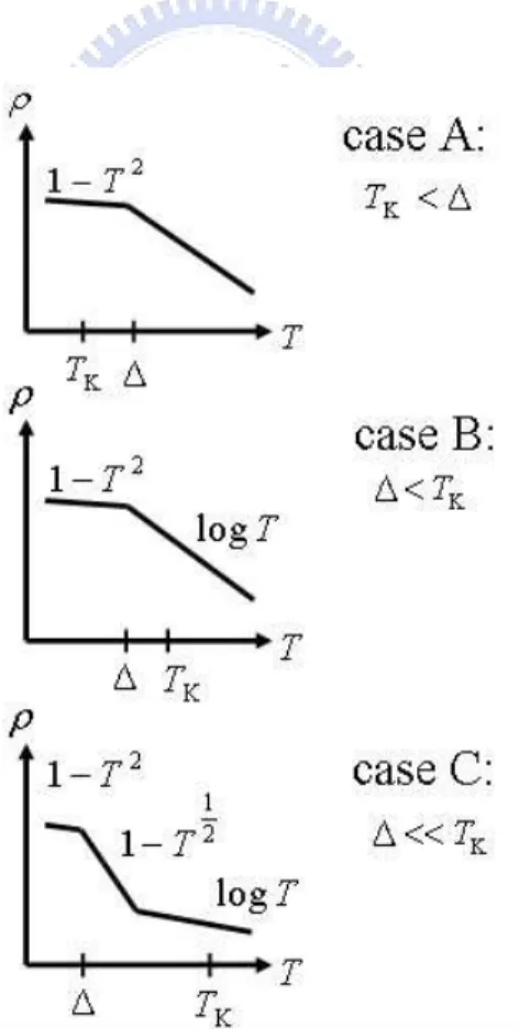
The electrical resistivity measures the electronic scattering rate off the TLS. This subject has been first discussed by Cochrane et. al.,(75) who introduced an ill-defined model with two sets of conduction electrons heuristically provided. The first calculation was performed by Kondo(76; 77) up to fourth order in-troducing the assisted tunneling. The resistivity behavior expected at different temperatures depends on the ratio of ∆0/TK, and this is illustrated in Fig. 2-7.
In the top curve of the Fig. 2-7, TK < ∆0 so that the Kondo correlated state is
3.3 Correction to Conductivity
Figure 3.6: A schema of two-level system.
3.3 Correction to Conductivity
curves of Fig. 2-7 we see the Fermi-liquid behavior developing eventually below
TK, but with a non-Fermi-liquid region possible provided that ∆0 ¿ TK.
At high temperatures, summation of the logarithmic divergent terms gives the correct logarithmic rise in ρ(T ). At low temperature for zero splitting of the levels, the non-Fermi-liquid excitation spectrum produces an anomalous saturation of the resistivity. According to conformal field theory and NCA, δρ(T ) ≈ ∆ρ(0)(1 −
aT1/2) in the weak-coupling limit, where a is a pure number that depends on the
Chapter 4
Experimental and Technical
Considerations
4.1
Introduction
In the measurement of the electron dephasing time at low temperature, we take several experimental techniques and considerations. We divide them into three parts and discuss them respectively. First part is techniques of preparing samples. Second part is low temperature measurement and last part is measuring circuit noise.
4.2
Sample Preparation
4.2.1
Substrate Cleaning
In our experiments, we use corning glass (number: 7059) as substrates. The width is 10 mm square and thickness is 0.3 mm. Before depositing films onto the substrates, we should clean the glass to avoid the unanticipated impurities on the surface. The cleaning processes are as follows. The substrates are cleaned in turn in trichloroethylene (TCE), acetone (ACE), and alcohol solvent for five minutes in an ultrasonic cleaner, and then the substrates are blown-dry with N2 gas. Once
finish the cleaning, a mask will be used to pattern the shape of films. In this series of experiments, we used two kinds of masks, metal mask and photolithography.
4.2 Sample Preparation
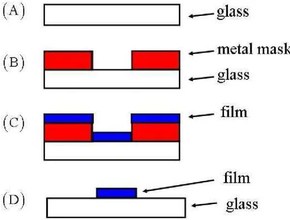
4.2.1.1 Metal Mask
The width and the length of the films are 0.4 mm and 5.7 mm, respectively. The film thickness are 195˚A ± 5˚A or 147˚A ± 3˚A. Figure 4.1 shows the processes of the deposition using metal mask. All of the cartons are at front view.
Step A: Preparing a clean glass.
Step B: The metal mask is plastered on the glass using a thin coat of Apiezon ’N’ vacuum grease.
Step C: Depositing the wanted material and thickness onto the mask and glass. The deposited thickness should be thinner than the mask to avoid the connecting between the films on glass and on the mask.
Step D: Remove the metal mask carefully. The patterned films are deposited on the substrate.
4.2.1.2 Photolithography
Because of the difficulty of manufacture of metal mask, the narrowest width which one can achieve is about 0.1 mm by using metal mask. When one needs narrower films, the photolithography technique can help us achieve it. The limit of the width of photolithography technique depends on wavelength of light. Typically, the narrowest width is about several µm. Figure 4.2 shows the processes of the photolithography technique. There are five steps to achieve it.
Step A: Coating a photoresist, a liquid polymeric material, onto the substrates. The coating process is performed by spinning the substrates at speeds several thousand rpm. Photoresist is deposited onto the substrate surface during the dynamic movement to ensure coating over the entire substrate surface. The coating thickness depends on the photoresist and spinning speeds.
Step B: Once the substrate has been coated with photoresist, putting the photo mask on the substrate and exposing the substrate on an exposure light. By shining light through the photo mask and onto the substrate, individual areas of the photoresist are selectively exposed to light. This exposure causes a chemical change in the photo resist.
Step C: Once exposed, the substrate is then immersed in a developer solution. Developer solution are typically aqueous and will dissolve away areas of the
pho-4.2 Sample Preparation
4.2 Sample Preparation
toresist that were exposed to light. Therefore, after successful development, the photoresist is patterned with the wanted shape.
Step D: Depositing the wanted material and thickness onto the mask and glass. The deposited thickness should be thinner than the mask to avoid the connecting between the films on glass and on the mask.
Step E: Remove the photoresist by acetone. The patterned films are deposited on the substrate.
4.2.2
Sputtering
All of our thin films are fabricated by sputtering deposition. Our source target is the Cu93Ge4Au3 (atomic rate). Before sputtering, we pump the chamber vacuum
to high vacuum. Once the vacuum reaches the order of 10−6 mbar, we inject 7
sccm argon gas into the chamber and the pressure increases to order of 1 × 10⁻³
mbar. Because our target is a good conductor, we chose a DC voltage source. The sputtering power ranges from 10 W to 110 W and it affects levels of the randomness (disorder) of the samples. The room temperature resistivity of our films range from 15 µΩcm to 95 µΩcm.
Here we would discuss a little bit the operating principles of sputtering. Sput-tering is a technique used to deposit thin films of a material onto a substrate. By first creating a gaseous plasma and then accelerating the ions from this plasma into a source target, the source material is eroded by the arriving ions via energy transfer and is ejected in the form of neutral particles. As these neutral particles are ejected they will travel in a straight line unless they come into contact with other particles or a nearby surface. If a substrate is placed in the path of these ejected particles it will be coated by a thin film of the source material.
The ”diode sputtering” example given above has proven to be a useful tech-nique in the deposition of thin films when the cathode is covered with sputtering target. Diode sputtering however has two major problems. First one is the depo-sition rate is slow and second one is the electron bombardment of the substrate is extensive and can cause overheating and structural damage.
The development of magnetron sputtering deals with both of these issues simultaneously. Figure 4.3 shows the schematic of the magnetron sputtering. By
4.2 Sample Preparation
4.3 Low Temperature Resistance and Magnetoresistance Measurement
using magnets behind the cathode to trap the free electrons in a magnetic field directly above the target surface, these electrons are not free to bombard the substrate to the same extent as with diode sputtering. At the same time the extensive, circuitous path carved by these same electrons when trapped in the magnetic field, enhances their probability of ionizing a neutral gas molecule by several orders of magnitude. This increase in available ions significantly increases the rate at which target material is eroded and subsequently deposited onto the substrate.
The ensuring process might be compared to a find sand blasting in which the momentum of the bombarding particles is more important than their energy. The inserted argon gas is chosen because it is a heavy rare gas and is plentiful. It also has a low ionization potential.
Figure 4.4shows the film by using photolithography. The width of the film is 50 µm. Silver plaster is used to stick four copper wires with diameter 50µm on the four electrodes with 0.5 mm square.
The talbe 4.1 shows the sputtering parameters for all films. The pressure is the chamber pressure during deposition and thinkness is the deposed thinkness of films. In the system, we use two kinds of mask, metal mask and photomask. The deposition rates are basically proportion to the sputtering powers.
4.3
Low Temperature Resistance and
Magne-toresistance Measurement
After finishing preparing the samples, we will mount our samples onto the cryo-stat to do low temperature transport measurement. In low temperature measure-ments, it is the first step for accurate measurements that electron temperature is the same as the thermometer temperature, otherwise the hot electron physics occur. There are two easy ways to confirm that whether the samples are real cooled down. First one is that the joule heat of the system, I2R, is much smaller
than the cooling power of refrigerator. The accuracy of the method is not high, because it does not take into account of the joule heat of the conducting wire and therm-conductivity between sample and sample holder. Second way, which