國 立 交 通 大 學
電子工程學系 電子研究所碩士班
碩 士 論 文
具有奈米線通道的矽鍺及雙閘極薄膜電晶體特
性分析
Characterizations of Silicon-Germanium and
Double-Gated Nanowire Thin-Film Transistors
研 究 生:洪振家
指導教授:林鴻志 博士
黃調元 博士
具有奈米線通道的矽鍺及雙閘極薄膜電晶體特性分析
Characterizations of Silicon-Germanium and Double-Gated
Nanowire Thin-Film Transistors
研 究 生:洪振家 Student:Jen-Jia Hung
指導教授:林鴻志 博士 Advisor:Dr. Horng-Chin Lin
黃調元 博士 Advisor:Dr. Tiao-Yuan Huang
國 立 交 通 大 學
電子工程學系 電子研究所碩士班
碩 士 論 文
A Thesis
Submitted to Institute of Electronics
College of Electrical Engineering and Computer Science National Chiao Tung University
in partial Fulfillment of the Requirements for the Degree of Master of Science
in
Electronic Engineering June 2006
具有奈米線通道的矽鍺及雙閘極薄膜電晶體之特性分析
研究生:洪振家 指導教授:林鴻志 博士
黃調元 博士
國立交通大學
電子工程學系 電子研究所
摘 要
在本篇論文中,我們製作了一種具有奈米通道的多晶矽和多晶矽
鍺薄膜電晶體,並且分析其特性。因為奈米線通道為多晶的結構,為
了更有效修補其中的缺陷及斷鍵,我們對元件使用了氨電漿的處理,
讓通道中的缺陷得到修補,使元件有更好的操作特性,例如:降低漏
電流、提升載子遷移率、增強開啟電流等。我們也分別分析並討論了
有關矽和矽鍺薄膜電晶體的漏電機制。雖然二種電晶體的結構相同,
但因為矽鍺通道中有較多的缺陷,造成主要影響漏電的區域不同,也
因此有著不同的漏電機制。
在本實驗中,我們也製作了具有雙閘極奈米通道的多晶矽薄膜電
晶體。雖然有著雙閘極的結構,但在製作過程中,並不需要添加額外
的光罩步驟,就能在通道上額外加上副閘極。雙閘極操作為將主閘極
和副閘極提供相同電壓,因為雙閘極對通道會有較好的操控能力,所
以雙閘極操作會有較好的元件特性。此外,我們可以藉著提供不同的
副閘極電壓,使臨界電壓隨之調變,且不論導通通道長短或是氨電漿
處理時間長短,臨界電壓的調變都是接近線性的。此外,在實驗中也
發現,副閘極可輔助主閘極使其在操作時對導通通道有更好的操作能
力,並使 DIBL 的效應降低。
Characterizations of Silicon-Germanium and
Double-Gated Nanowire Thin-Film Transistors
Student: Jen-Jia Hung Adviser: Dr. Horng-Chih Lin
Dr. Tiao-Yuan Huang
Department of Electronics Engineering & Institute of Electronics
National Chiao Tung University
Abstract
In this thesis, we fabricated a novel TFT with nanowire channels and analyzed
its characteristics. In order to improve the device performance, we performed the NH3
plasma treatment to passivate defects, reduce leakage current, enhance carrier
mobility, increase driving current and decrease subthreshold slope. We also analyzed
and discussed the leakage mechanisms of TFTs with Si and SiGe channels. SiGe films
are found to contain more traps and defects which lead to worse characteristics as
compare with their poly-Si counterparts. In addition, the major leakage paths of the
poly-SiGe devices are found to be different from those in the poly-Si ones.
proposed and demonstrated. The fabrication of such double-gated structure does not
require extra mask. When the main-gate and sub-gate are tied together, denoted as the
double-gated mode, the TFT performance is improved. It is also shown that threshold
voltage can be modulated by varying the sub-gate voltage, and the modulation in Vth
shows linear dependence on the applied sub-gate bias regardless of channel length or
plasma passivation time. The sub-gate can also reduce DIBL effect by assisting the
誌 謝
首先,感謝我的指導教授黃調元博士及林鴻志博士,在二人細心的指導與教 誨之下,這本論文才得以完成。他們二人專業上豐富的知識,研究上嚴謹的分析, 私下幽默風趣的言談,最重要的是從他們做事的態度及研究的精神,使我在心靈 上有著極大的成長,懂得如何獨立思考及解決問題,令我獲益良多。 其次,我要感謝實驗室的學長們。首先是帶著我做實驗及研究分析的李明賢 學長及蘇俊榮學長,阿賢學長有條不紊的做事態度及豐富的實做經驗,阿榮學長 對研究的投入和熱忱,都是我學習的榜樣。感謝呂嘉裕學長及李耀仁學長在實驗 上的幫助及研究上的建議。此外,葉冠霖學長、盧文泰學長、林宏年學長、盧景 森學長、張尹鋒學長、房新原學長、林賢達學長、李聰杰學長、藍文廷學長,感 謝你們對我的教導與鼓勵。還要感謝國家奈米實驗室所有的工程師及員工,因為 有你們細心維護機台,提供了完善的環境及良好的設備,使我能順利完成實驗。 再來,我要感謝我實驗室的同學,謝雨霖、蔡銑泓、趙志誠、黃健銘、張凱 翔、徐行徽、呂建松。有你們的扶持,讓我做研究不再孤單,有你們的陪伴,讓 我充滿了許多美好的回憶,因為有了你們,使的實驗室除了是研究的地方外,更 是充滿溫情及歡笑的地方,很高興和你們度過了這美好的時光。 另外,我要特別感謝我從高中就認識的好兄弟王壽愷、黃名碩、李振瑋、曾 思衡、李昇達。在新竹念書有你們的陪伴,讓我倍感溫馨。 最後,我要感謝我的家人,給了我最大的支持及鼓勵,是我得以完成碩士的 學位最大的功臣。要感謝的人太多,還有許多是上述所沒提到的,在此致上最誠 摰的歉意及無限的謝意。再次感謝所有的陪我一路走來的人,謝謝。Contents
Abstract (in Chinese) ... i
Abstract (in English) ... iii
Acknowledgement (in Chinese) ... v
Contents ... vi
Table Captions... viii
Figure Captions ... ix
Chapter 1 Introduction... 1
1-1 Overview of the Polysilicon Thin-Film Transistors... 1
1-2 Silicon-Germanium Applications for Low-Temperature Polycrystalline Thin-Film Transistors... 3
1-3 Overview of Nanowires... 4
1-4 Introduction of Double-Gated Thin-Film Transistors... 7
1-5 Thesis Organization ... 9
Chapter 2 Device Fabrication and Operation Principles ...11
2-1 Device Structure and Fabrication ...11
2-2 Device Measurements and Operation of the Nanowire Thin-Film Transistors... 13
Chapter 3 Silicon-Germanium Nanowire Thin-Film Transistors... 16
3-1 Basic Device Characteristics of Nanowire TFTs ... 16
3-2 Characteristics for Poly-Si and Poly-Sil-xGex Nanowire TFTs ... 17
3-3 The Activation Energy ... 18
4-1 Operation Modes of Double-Gated Nanowire TFTs ... 23
4-2 Device Characteristics with Various Sub-Gate Biases... 25
Chapter 5 Conclusions and Future Work ... 28
5-1 Conclusion ... 28
5-2 Future Work ... 29
Table Captions
Table 2-1 NH3 plasma treatment conditions. ... 41
Table 3-1 Key parameters of the silicon-germanium nanowire TFTs with
different NH3 plasma passivation times... 42
Table 3-2 Summary of key parameters for n-type poly-Si and poly-Sil-xGex
nanowire TFTs at VD = 0.5 V. ... 43
Table 3-3 Summary of key parameters for p-type poly-Si and poly-Sil-xGex
nanowire TFTs at VD = 0.5 V. ... 43
Table 4-1 Characteristics of nanowire TFT with DG and SG operations. ... 44 Table 4-2 Improving DIBL effect by varying sub-gate voltage. ... 44
Figure Captions
Figure 2-1 Definition of the main gate... 45
Figure 2-2 Deposition of LPCVD TEOS and channel layer. ... 45
Figure 2-3 Ion implantation. ... 45
Figure 2-4 Self-aligned formation of nanowire channel. ... 46
Figure 2-5 Deposition of passivation oxide layer. ... 46
Figure 2-6 Definition of sub-gate. ... 46
Figure 2-7 Top view of nanowire TFT with double-gated structure... 47
Figure 2-8 (a) Cross sectional picture of sidewall spacer nanowire channel of poly-Si TFT. ... 48
Figure 2-8 (b) Cross sectional picture of sidewall spacer nanowire channel of poly-Si TFT. ... 49
Figure 2-8(c) Cross sectional picture of sidewall spacer nanowire channel of poly-SiGe TFT... 49
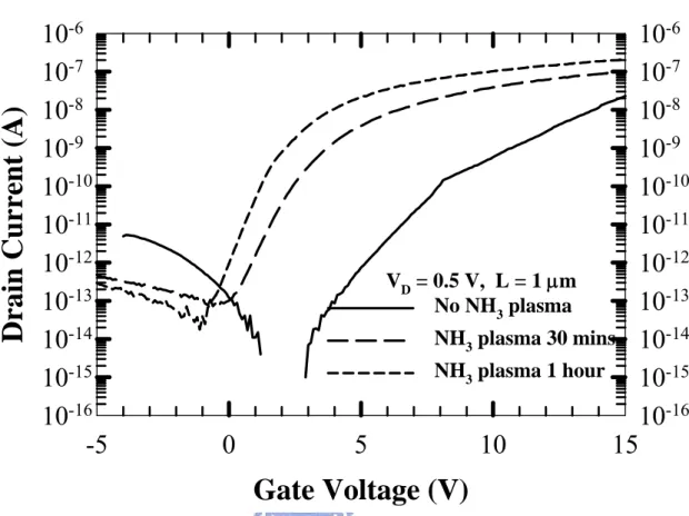
Figure 3-1 Transfer characteristics of silicon-germanium nanowire TFTs with different NH3 plasma passivation times. ... 50
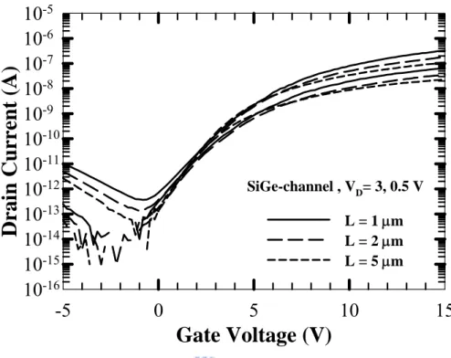
Figure 3-2 Transfer characteristics of poly-Sil-xGex nanowire TFT with different channel lengths. ... 51
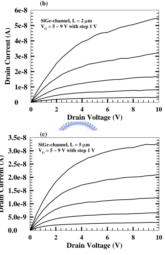
Figure 3-3 (a) Output characteristics of a typical poly-Sil-xGex nanowire TFT with channel length of 1 μm... 51
Figure 3-3 Output characteristics of poly-Sil-xGex nanowire TFTs with channel length of (b) 2 μm and (c) 5 μm. ... 52 Figure 3-4 Off-state current with various gate widths in (a) poly-Si and (b)
Figure 3-5 Top view of nanowire TFT with double-gated structure and the
location of major leakage current induced region. ... 54 Figure 3-6 Typical transfer characteristics of n-type poly-Si and poly-Sil-xGex
nanowire TFTs. ... 55 Figure 3-7 Typical transfer characteristics of p-type poly-Si and poly-Sil-xGex
nanowire TFTs. ... 55 Figure 3-8 Off-state leakage of poly-Sil-xGex nanowire TFT at drain voltage (a)
0.5V and (b) 3 V at various temperatures. ... 56 Figure 3-9 Dependency of activation energy for poly-Sil-xGex nanowire TFT on
gate and drain voltage... 57 Figure 3-10 Off-state leakage characteristics of n-type (a) poly-Si and (b)
poly-Sil-xGex nanowire TFTs characterized at various temperatures.
... 58 Figure 3-11 Dependency of activation energy on gate voltage for poly-Si and
poly-Sil-xGex nanowire TFTs... 59
Figure 3-12 Extracted DOS results in poly-Si and poly-Sil-xGex nanowire TFTs
with channel length of 1 µm. ... 60 Figure 4-1 Transfer characteristics of a typical nanowire TFT under single- and
double-gated operations... 61 Figure 4-2 On-state drain current as a function of channel length under different
modes of operation. ... 62 Figure 4-3 The ON current improvement as a function of the channel length.... 62 Figure 4-4(a) Output characteristics of a typical nanowire TFT under single- and
double-gated operations with L= 0.8μm... 63 Figure 4-4(b) Output characteristics of a typical nanowire TFT under single- and
Figure 4-4(c) Output characteristics of a typical nanowire TFT under single- and double-gated operations with L= 5 μm... 64 Figure 4-5 (a) ID-VG characteristics with various sub-gate biases, (b) the modified
curves obtained by subtracting IOFF @ Vsub = -4 V... 65
Figure 4-6 Vth modulation with Vsub varying from 4 to -4 V in steps of 1 V for
different channel lengths. ... 66 Figure 4-7 (a) Vth modulation with Vsub varying from 4 to -4 V in steps of 1 V
with different NH3 plasma times, (b) the dependence of average Vth
shift per Vsub... 67
Chapter 1
Introduction
1-1
Overview of the Polysilicon Thin-Film Transistors
Polycrystalline silicon thin-film transistors (TFTs) have attracted much
attention since its first demonstration in 1966 [1]. Over the past thirty years, poly-Si
TFTs have been proliferated to a wide range of industrial applications including
active-matrix liquid-crystal displays (AMLCDs) [2], [3], thermal printer heads [4],
linear image sensors [5], [6], scanners [7] and photo-detector amplifier [8], as well as
VLSI memories, such as dynamic access memories (DRAMs) [9], static random
access memories (SRAMs) [10], [11], electrical programming read only memories
(EPROMs) [12], and electrical erasable programming read only memories
(EEPROMs) [13], [14]. In particular, the application in AMLCDs is the major force to
promote and advance the development of poly-Si TFT technology.
AMLCDs are one of the most promising candidates for realizing high-quality
large-area flat-panel display. AMLCDs initially relied predominantly on n-type α-Si
TFTs. But the low electron field-effect mobility limits on-state current and thus
results in unacceptable electric performance for integration of driver circuitry. The
and higher drive capability of poly-Si TFTs enable the integration of driver circuitry
on the display panel [15], which further improves system performance and reliability
[16], [17]. Thus, poly-Si TFTs become the de facto choice for high performance
AMLCD applications. Unfortunately, the high temperature process (>600 ℃ )
employed in conventional methods for the fabrication of poly-Si TFTs excludes the
use of cheap glass as the starting substrate. Therefore, reducing the process
temperature or the process time is very important for poly-Si TFT technology. To this
date, there are several useful methods proposed and applied in the fabrication of TFT
technology to reduce thermal budget, such as solid-phase crystallization (SPC)
[18], [19], laser annealing [20], [21], metal-induced lateral crystallization (MILC)
[22], [23], rapid thermal annealing (RTA) [24]- [26], and so on.
Polycrystalline silicon is rich in grain-boundary defects as well as intragrain
defects, and the electrical activity of these charge-trapping centers profoundly affects
the thin film transistor characteristics. The electrical properties of polycrystalline
semiconductor devices are strongly affected by the defects such as dangling bonds
and strained bonds located at or near the grain boundaries [27]. The high density of
defect states at grain boundaries and interior of grains may lead to poor performance
such as degraded mobility, poor subthreshold swing, large threshold voltage, and large
high-performance poly-Si TFTs, it is necessary to reduce the trap-states of the
polysilicon films. It is now well known that hydrogenation tends to tie up the
grain-boundary dangling bonds with hydrogen, thereby remarkably improving the
characteristics of the poly-Si TFTs [28]. Recently, it has been reported that the H2/N2
mixture plasma and nitrogen ion implantation significantly improve the electrical
characteristics of the poly-Si TFTs [29], [30]. Tsai et al. showed that the
nitrogen-containing hydrogen plasma treatment could further improve the
characteristics of the TFTs as compared with pure H2 plasma treatment [29]. It is
found that TFTs after the NH3-plasma passivation depict better device performance
[31], including lower off-current, better on/off current ratio, and better hot-carrier
reliability, compared with the H2-plasma treated counterparts.
1-2 Silicon-Germanium Applications for Low-Temperature
Polycrystalline Thin-Film Transistors
The usage of relatively cheap glass substrates further reduces manufacturing
cost. However, it places tighter constraints on the thermal-budget allowance for a TFT
fabrication process, due to problems associated with glass shrinkage and warp. The
fabrication of high-performance poly-Si TFTs typically requires high-temperature or
problem can be addressed through the use of silicon-germanium (Sil-xGex) films. The
major advantages of Sil-xGex are low processing temperature, adjustable bandgap, and
compatibility with Si-based processing technology. Due to lower thermal budget and
higher carrier mobility, poly-Sil-xGex has been recently used as an alternative to
poly-Si for TFT applications. Poly-Sil-xGex TFTs fabricated by low-temperature solid
phase crystallization have been demonstrated. Dopants can be activated at lower
temperature in Sil-xGex thin films than in Si [32], [33]; therefore, a lower thermal
budget can be used to fabricate poly-Sil-xGex, TFTs compared with poly-Si TFTs on
glass substrates.
Although the fabrication process of poly-Sil-xGex TFTs is almost compatible
with that of conventional poly-Si TFTs, some unexpected issues might arise from the
different intrinsic properties of Si and Ge. The carrier mobilities are too low for
practical applications [34]. The low carrier mobilities are attributed to the high
trapping-state density at grain boundaries found in the poly-Sil-xGex films, which is
caused by the binary nature of the SiGe system. Therefore, the process should be
modified to avoid degrading the device performance. NH3-plasma passivation can
also improve device performance.
The semiconductor nanowire represents a particular interesting material system.
It can be produced with precisely controlled chemical composition, physical
dimension and electronic properties, and can function both as interconnect and critical
device elements. It has recently been demonstrated that individual nanowire can be
used to fabricate nanoscale field-effect transistor with electronic performance
comparable to or even exceeding that of the highest-quality single-crystal material
[35], [36]. Furthermore, functional logic gates and computational circuits have also
been assembled [37], [38]. These nanocircuits promise to push the Moore's law to the
ultimate limit with unprecedented performance. However, it is very difficult to
implement production-scale nanoelectronics currently due to the complicated and
limited scalability of the fabrication processes used. Many high-performance TFTs
have been demonstrated on various substrates including plastics [39], [40]. These TFTs
have a conducting channel consisting of multiple single crystal nanowires in parallel,
or a single crystal nanoribbon, spanning the full distance from source to drain, thus
assuring high carrier mobility. Both p- and n-channel TFTs have been demonstrated
with carrier mobility approaching that of single crystal materials [41], and acceptable
ON/OFF ratios and subthreshold swing.
Preparation of Si nanowires could be classified mainly into two types, namely,
The top-down approach uses advanced lithography techniques, such as deep UV,
e-beam or nanoimprint, to generate the nanowire patterns, followed by an etching step
to obtain the nanowire structures. These techniques are well developed and mature for
mass production purpose. Nevertheless, very expensive equipments and cutting-edge
techniques are required. Conventional photolithography processes, though relatively
cheap for manufacturing, are not capable of patterning nanowires directly. Some
special skills such as thermal flow, chemical shrink, and spacer patterning have been
proposed to help generate the nano-scale patterns using these conventional
lithography tools.
The bottom-up approach typically utilizes deposition methods to prepare the
nanowires, and synthesize the nanowires on a substrate. Later in the process these
nanowires were harvested and dispersed into a solution. Depositing the harvested
nanowires onto another oxidized substrate and making electrical contacts to the
nanowires complete the device structure. Many deposition methods have been
developed nowadays which include laser ablation catalyst growth [42], chemical
deposition catalyst growth [43] and oxide-assisted catalyst-free method [44]. The first
two methods are carried out with metal nanocluster catalyst as the energetically
favored sites for absorption of gas-phase reactants, and then the cluster supersaturates
potential concern in the catalyst approaches. Oxide-assisted catalyst-free method is
conducted without metal nanocluster catalyst, and thus is free from metal
contamination. Nevertheless, there could be plenty of defects in the wires, and hence
it is not applicable to electronic devices.
Alignment of nanowires could be achieved with the aid of an applied electric
field in the bottom-up schemes. Although electric fields enable more control over
assembly, this method is limited by electrostatic interference between nearby
electrodes. The requirement of extra lithography and etch steps in fabricating the
electrodes are needed. Moreover, the control of doping concentrations in
self-assembled semiconducting nanowire remains a challenge, and it’s difficult for
high-density integration.
Although most of the aforementioned issues could be avoided in the top-down
approaches, usually expensive lithography apparatus and materials are used in this
category of nanowire preparation that dramatically increase the fabrication cost. In
this study, to circumvent these shortcomings, we propose to develop a new method for
preparation and fabrication of Si and Sil-xGex nanowire TFT devices.
1-4 Introduction of Double-Gated Thin-Film Transistors
semiconductor industry. The concept of device scaling has consistently resulted in
better device density and performance. In conventional MOSFETs, control of
short-channel effects for scaled devices requires very thin gate dielectrics and high
doping concentrations. After decades of devices scaling, some physical limitations of
CMOS technology are approaching. As a consequence, the need arises for alternative
device structures. Many novel structures have been proposed for the nanoscale
devices. One such structure is the Double-Gate Transistor (DGT), first demonstrated
in the 1980s [45]. Other possible solutions include SOI devices [46], [47],
strained-silicon FETs [48], [49], carbon nanotube FETs [50], [51], etc. DGT is
composed of a conducting channel DGT, surrounded by gate electrodes on two
opposite sides. This ensures that no part of the channel is far away from a gate
electrode. The voltage applied on the gate terminals effectively controls the channel
potential, and positively enhance the controllability of gate bias on the device
switching.
Nowadays high-performance TFT technologies have been investigated and
widely used in advance IC industry. However, the performance of conventional
poly-Si TFT is far from satisfactory in terms of speed and current drive [52]. It has
been experimentally demonstrated that double-gated TFTs can provide a higher ON
slope [53], [54]. While double-gated structure is attractive, the fabrication of
high-performance double-gated device is difficult. Therefore, TFT with nanowire
channel is an alternative approach to improve device properties [55]. Due to its small
volume, fewer defects and grain boundaries exist in poly-Si nanowires, leading to
lower leakage current, higher carrier mobility and better S.S. Also owing to the tiny
body of nanowire, the gate can exhibit stronger control over the channel resulting in
improved short channel effects [55].
The fabrication of the double-gated TFT is difficult, however. With the
exception of FinFET, alignment of both gates is not easy to achieve. Misaligned gates
result in extra capacitance and loss of current drive. Several different structures have
been proposed to deal with fabrication issues, including planar and quasi-planar
structures.
1-5 Thesis Organization
This thesis is divided into five chapters. In Chapter 2, we briefly describe the
device structure, fabrication flow, and electrical characterization methods for the
devices. Then, we present the results on characterizing the operation of the
double-gated nanowire TFT in Chapter 3. The poly-Sil-xGex nanowire TFTs are
Chapter 2
Device Fabrication and Operation
Principles
2-1 Device Structure and Fabrication
First, silicon wafers capped with a buffer silicon dioxide layer were used as the
starting substrate. A 1000 Å n+-doped poly-Si layer was first deposited on the starting
substrate serving as the gate electrode (Fig. 2-1), followed by the deposition of a
chemical vapor deposition (CVD) oxide layer with a thickness of 400 Å serving as the
gate dielectric. A 1000 Å channel layer was then deposited on the gate dielectric (Fig.
2-2). Wafers were then split to receive either α-Si or α-Sil-xGex to serve as the channel
layer. Next, an annealing step was performed at 600 ℃ in N2 ambient for 24 hours to
transform the α-Si or α-Sil-xGex into polycrystalline. Subsequently, source/drain (S/D)
implant was performed with P+ for n-type TFTs and BF
2+for p-Type TFTs at 10 keV
and 1×1015cm-2 (Fig. 2-3). Note that the implant energy was kept low so that most of
the implanted dopants were located near the top surface of the Si and Sil-xGex layers.
S/D photoresist patterns were then formed on the substrate by a standard lithography
step. A reactive plasma etch step was subsequently used to remove the channel layer,
The implanted dopants were removed in this etch step except in the S/D regions. Due
to the low implantation energy, the channel would remain undoped. After channel
formation, a 2000 Å tetraethylorthosilicate (TEOS) layer was formed by LPCVD
process to serve as the passivation layer (Fig. 2-5) and also as the gate dielectric of the
sub-gate in some samples. Standard metallization (aluminum 5000 Å) steps were next
performed to form the sub-gate as well as test pads (Fig. 2-6). The deposition of
TEOS is carried out at 720 ℃ in a furnace for about 2 hours and the dopants can be
activated at this step. After sintering at 400℃ in N2/H2 ambient for 30 minutes, the
device processing was completed. Since it is known that TFTs with poly-Si and
poly-Sil-xGex channels depict improved electrical characteristics after NH3 plasma
treatment [31], some devices were subjected to several hours of NH3 plasma treatment
before characterization. The plasma treatment condition is shown in Table 2-1.
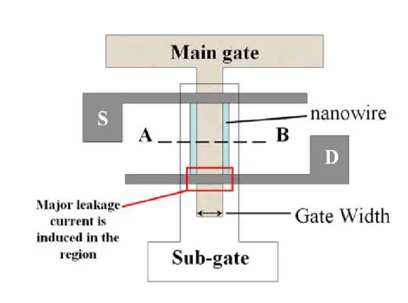
Top view of the nanowire TFT is shown in Fig. 2-7, while the cross-section
view of the new device along A-B is shown in Fig. 2-6. In the proposed structure, the
mask count is only four. Specifically, the mask count consists of the main gate mask,
source/drain mask, contact hole mask and metal pad mask in this work. The nanowire
channel was formed simultaneously with the source/drain regions and we could define
the nanowire channel easily because of the self-aligned manner. Moreover, the
electrical property by changing over-etching time.
Fig. 2-8 shows the SEM pictures of a fabricated poly-Si TFT. In Fig. 2-8 (a), the
cross-sectional view of the poly-Si TFT with gate width of 1 μm and two nanowire
channels located alongside the main-gate. The enlarged views shown in Fig. 2-8 (b) (c)
indicates that the thickness and width of the nanowire channel are around 30 nm to 40
nm, respectively.
2-2 Device Measurements and Operation of the Nanowire
Thin-Film Transistors
The electrical performance of TFTs strongly depends on the structural
parameters and quality of the channel layer. Two important parameters for the
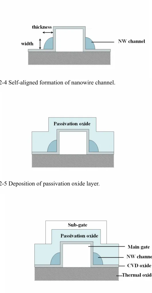
nanowire channels, namely, the width and thickness of the channel, are defined in Fig.
2-4. The width and thickness of the sidewall channel both depend on the gate height,
thickness of the deposited channel layer, and etching time for our poly-Si nanowire
TFTs. Gate height as well as the as-deposited channel thickness are reduced to shrink
the nanowire dimensions without resorting to time-consuming over-etching technique.
Over etching time is another major parameter for controlling the nanowire structure.
The operation principles of our new nanowire TFTs are similar to those of the
positively biased with respective to the source, and the gate bias is higher than the
threshold voltage, the device is turned on. On the other hand, when the gate bias is
smaller than the threshold voltage, the device is turned off. In contrast to conventional
TFTs in terms of structural arrangement, our nanowire channels are aligned along the
sidewall of the gate.
The parameters of the transistors and I-V characteristics, including threshold
voltage (Vth) and subthreshold swing (SS), were measured and extracted using an
HP4156 parameter analyzer.
The on-current in the linear region (VG > Vth, VG-Vth > VD) can be expressed as:
(
)
1 2 2 D O X G th D D W I C V V V V Lµ
⎡ ⎤ = ⎢ − − ⎥ ⎣ ⎦ (2-1)where L is the channel length, W is the channel width, µ is the mobility, and Cox is the
gate capacitance per unit area. The on-current in the saturation region (VG > Vth,
VG-Vth < VD) can also be expressed as:
(
)
21
2
D O X G thW
I
C
V
V
L
µ
⎡
⎤
=
⎣
−
⎦
(2-2)Each nanowire TFT device has two channels that must be taken into account in
the analysis of the I-V characteristics or mobility extraction.
The transconductance, Gm, is extracted by the differentiation of equation
(2-1), D D M V const O X D G
I
W
G
C
V
V
=L
µ
∂
⎛
⎞
=
= ⎜
⎟
∂
⎝
⎠
(2-3)Subthreshold swing (SS) can be calculated from the subthreshold current,
(
log
) (
10
) ( )
2.3
(
)
G G G D D DI
I
I
SS
ln
I
lnI
lnI
∂
∂
∂
=
=
=
∂
∂
∂
(2-4)These electrical parameters could be extracted from the ID-VG curves under a
Chapter 3
Silicon-Germanium Nanowire
Thin-Film Transistors
3-1 Basic Device Characteristics of Nanowire TFTs
One of the main merits associated with the fabrication of poly-Sil-xGex TFTs are
the lower deposition temperature of Sil-xGex film than silicon film, and thus the
requirement of lower thermal budget in the fabrication process. Lower temperature is
needed for dopant activation in Sil-xGex thin films than in Si. However, the binary
nature of the Si-Ge system complicates the optimization substantially. Higher
trapping-state density and defects at grain boundaries are found in the poly-Sil-xGex
films. Therefore the NH3-plasma passivation is often employed to achieve better
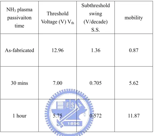
device performance. Fig. 3-1 shows the poly- Sil-xGex nanowire TFTs with different
NH3 plasma passivation times. The device performance such as leakage current, the
ON-state current, subthreshold swing, and the mobility, are all improved as the
plasma time increases. Detailed parameters are listed in Table 3-1.
The transfer characteristics of poly-Sil-xGex nanowire TFTs with different
channel lengths are shown in Fig. 3-2. The short-channel effect seems not significant
different from that found in the poly-Si case and is attributed to the existence of a high
amount of defects in silicon-germanium film. Fig. 3-3 shows the output characteristics
of poly-Sil-xGex nanowire. Well-behaved device performance is achieved in these
devices.
3-2 Characteristics for Poly-Si and Poly-Si
l-xGe
xNanowire
TFTs
Fig. 3-4 (a) shows the I-V characteristics of poly-Si nanowire TFTs with
different gate widths. The definition of the nanowire TFT’s gate width is given in Fig.
2-7. It has been found that primary leakage paths in the poly-Si nanowire TFTs are
located in the top gate-to-drain overlap region. As the gate width increases, the
leakage current increases gradually as shown in Fig. 3-4 (a). This mechanism will be
discussed in more detail in Chapter 4. However, Fig. 3-4 (b) shows the I-V
characteristics of poly- Sil-xGex nanowire TFTs with different gate widths. The current
of poly-Sil-xGex nanowire TFTs shows little difference in off-region and it reveals that
the gate width does not dominate the major mechanism for the leakage in
poly-Sil-xGex nanowire TFTs. From Fig. 3-2, the TFTs have the same gate width but
different channel lengths. It shows that the leakage increases as channel length
poly-Sil-xGex nanowire TFTs is in channel region, as shown in Fig. 3-5. Although
these two types of TFTs have the same structure but they depicts different leakage
mechanisms because of the different amount of defect density contained.
Fig. 3-6 shows the comparison of voltage-current characteristics between n-type
poly-Si and poly-Sil-xGex nanowire TFTs. The poly-Si TFT exhibits better
subthreshold swing and higher ON-state current than poly-Sil-xGex TFTs because of
the better channel quality as mentioned above. Detail parameters such as threshold
voltage, subthreshold swing and mobilities are shown in Table 3-2. Transfer
characteristics for p-type nanowire TFTs are shown and compared in Fig. 3-7. The
p-type TFTs show much worse device performance than the n-type TFTs. It is
presumably due to the non-optimized S/D doping conditions. Note the gate electrodes
formed in this fabrication process was in-situ-doped n+ polycrystal silicon and the
channels remain undoped. This would result in higher threshold voltage in p-type
TFTs. Detail results are summarized in Table 3-2 and Table 3-3.
3-3 The Activation Energy
The off-state leakage current shows a strong dependence on the voltage
difference between the gate and drain, VGD, indicating that it is sensitive to the field
we have to understand the activation energy (Ea) in the off-state region. The activation
energy of the off-state can be obtained from the measurements of drain current at
different temperatures. The governing equation of off-state current, activation energy,
and temperature is given by
a E -k T o ff 0 I = I e (3-1)
where I0 is a constant independent of temperature, and Ea is the activation energy of
drain current.
The equation also can be expressed as
a off 0 -E ln (I )=ln(I )+ kT ⎛ ⎞ ⎜ ⎟ ⎝ ⎠ (3-2)
The off-state current characterized at various temperatures ranging from 25 ℃ to 125 ℃ in step of 25 ℃ under drain voltage of 3 V and 0.5 V are shown in Fig. 3-8.
Fig. 3-9 shows the dependence of Ea on gate and drain voltages. It is seen that the
activation energy decreases with increasing │VGD│, and results in larger off-state
TFT’s at various temperatures are shown in Fig. 3-9. Fig. 3-11 shows the dependence
of the extracted activation energy as a function of the gate voltage. In the subthreshold
region, the Ea for poly-Si nanowire TFTs shows a drastic drop with increasing gate
voltage. On the other hand, the drop is gradual for poly--SiGe nanowire TFTs. The
results indicate that a much higher amount of defects are contained when poly-SiGe is
used to replace the poly-Si as the nanowire channels. This also results in higher
threshold voltage in the poly-SiGe devices.
3-4 The Band-Gap DOS Analysis
The performance of poly-Si TFTs is strongly affected by defects contained in the
poly-Si channel. Characterization and analysis of density of gap states (DOS) are thus
essential for understanding the device characteristics and their dependence on the
processing conditions. Moreover, accurate DOS extraction is required for the
modeling of poly-Si TFT characteristics. In line with this, it has been shown that field
effect conductance [56], [57]method can serve this purpose.
FEC method was original proposed for characterizing the DOS in a-Si TFTs. When
applied to poly-Si TFTs, the presence of grain boundaries in the channel could be of a
great concern. Fortunately, it has been proven that, when the grain size is small
approach [56], in which the existence of grain boundary defects and intragranular
defects is assumed to be uniformly distributed throughout the material.
First, the temperature method [58] is used to determine the flat band voltage (VFB),
where the VFB is determined as the gate voltage where T(dlogG/dVG) is temperature
independent. This method is based on the temperature dependence of dG/dVG, where
G is the field conductance. Then the incremental method [59] is used to find the
relationship between ψS and VG.
From the FEC method the gap-state density is given by
2 2 2 0 ( ) 2 Si F S x S d Ng E q dx ε ψ ψ ψ = ⎛ ⎞ ∂ + = ⎜ ⎟ ∂ ⎝ ⎠
The electric field at the semiconductor surface is given, in the absence of surface
states, 0 . . OX OX OX G FB S x Si OX Si OX V V V d dx t t ε ε ψ ψ ε ε = − − = − = −
energy level in poly-Si and poly-Sil-xGex nanowire TFTs. The DOS in poly-SiGeis
higher than that in poly-Si TFT. Note that the tailed DOS is overestimated due to the
Chapter 4
Characterization of Double-Gated
Nanowire Thin-Film Transistors
4-1 Operation Modes of Double-Gated Nanowire TFTs
Double-gated structure is an attractive means for producing high-performance
and ideal silicon metal-oxide-semiconductor field-effect transistors. These devices
have a larger current drive, a steeper subthreshold slope, and a better control over the
short-channel effect. Such advanced structure is also applicable to poly-Si thin-film
transistors to enhance performance, as long as suitable structural device parameters
are implemented.
We fabricate and characterize the double-gate devices in this work. These
nanowire TFTs can be operated either in single-gated (SG) or double-gated (DG)
mode. In SG mode, the sub-gate electrode is floating, whereas in DG mode, the
main-gate and sub-gate electrodes are connected together to serve as the control gate.
Fig. 4-1 shows the transfer characteristics for operations in SG and DG modes. It is
clear to see that the performance is enhanced in terms of larger ON/OFF current ratio
and better S.S. under DG mode of operation. The field-effect mobility (extracted at
Major electrical characteristics are shown in Table 4-1.
Fig. 4-1 also shows the characteristics of operation with grounded sub-gate.
According to the SG characteristics, the nanowire TFTs are operated like the
depletion-type (i.e., normally ON) MOSFET devices, the channels near the sub-gate
side would turn on as the sub-gate is grounded and thus the effective inversion width
becomes larger. The threshold voltage of the normally ON nanowire devices shifts left
when the sub-gate is grounded. Although these nanowire TFTs are normally ON, the
channel of the devices are so thin that the carriers accumulate in the sub-gated channel
could be effectively depleted and turned off by the main-gate bias. Fig. 4-2 shows the
relationship between ON current and channel length at VD = 0.5 V, VG = 5 V. The DG
mode has a higher ON current than SG mode and sub-gate-grounded mode, because
of the better control of the channel potential by the gate bias. The larger effective
inversion width in sub-gate grounded mode results in higher ON current than the SG
mode. The ON current improvement as a function of channel length at VD = 0.5V, VG
= 5 V is given in Fig. 4-3. The increase in ON current in DG mode is higher than that
in SG modes with sub-gate floating or being grounded. As the channel length
increases, the ON current improvement decreases.
Figs. 4-4 (a), (b), (c) show the output characteristics of devices with different
increases. From Fig. 4-4 (a), the ID of DG mode with channel length of 0.8μm at VD
= VG = 5 V is 1.97 times that of SG mode. It is 3.48 times with channel length of
5μm shown in Fig. 4-4 (c). These improvements are mainly ascribed to a stronger
gate control under DG mode.
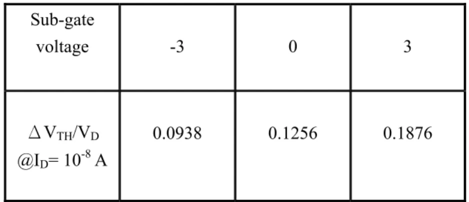
4-2 Device Characteristics with Various Sub-Gate Biases
In addition to DG operation, the sub-gate bias can also be independentlyapplied and be used to modulate the Vth of nanowire channels. Fig. 4-5 (a) shows the
ID-VG curves by varying the sub-gate voltage (Vsub) from 4 V to -4 V. In the OFF
region, all the IOFF at different Vsub coincide with each other, indicating that the
leakage mechanism is not dependent on the sub-gate bias. It has been found that
primary leakage paths are located in the top gate-to-drain overlap region [55], as
depicted in Fig. 2-7. The electric field between source and drain increases the band
bending and may enhance the tunneling probability of electrons from the valence
band to the conductance band via the trap states. The IOFF is mainly dependent on the
gate width which is also defined in Fig. 2-7. However, Imin becomes higher with more
positive Vsub, due proesumably to the higher electric field between drain and gate
when the curve shift left and result in increase of leakage current. To examine this
in Fig. 4-5 (b). The result reveals that all the curves have essentially the same Imin. The
on-state is mainly controlled by both main-gate and sub-gate, and the off-state is
dominated by the top gate-to-drain overlap region as mentioned above. On the other
hand, it is also found that the Vth is linearly modulated with the applied sub-gate bias,
as depicted in Fig. 4-6. The results indicate that the Vth modulation capability per unit
Vsub is smaller for longer channel devices than the shorter channel ones. Such
phenomenon is not well understood at this stage and more efforts are in progress to
investigate the issue. In short, Vth could be tuned to a suitable range in a reliable
manner.
Fig. 4-7 (a) shows the ID-VG curves by varying sub-gate voltage for devices
with different NH3 plasma treatment times. It is found that the TFTs after the NH3
plasma passivation achieve better device performance, suggesting that less active
defects remain in TFTs with longer passivation time. The Vth is linearly modulated by
the applied sub-gate bias with different NH3 plasma treatment times, as depicted in
Fig. 4-7 (b). The shift in Vth with varying sub-gate biases decreases for devices
receiving longer passivation treatment, owing to the reduction in the amount of the
active defect density.
It has been experimentally demonstrated that double-gated structure is capable
improve the drain-induced barrier lowering (DIBL) effect, as shown in Fig. 4-8.
Chapter 5
Conclusions and Future Work
5-1 Conclusion
In this work, we have fabricated and characterized the performance of TFTs
configured with a nanowire structure. The nanowire channels in the TFT devices were
formed by using a sidewall spacer etching technique. The fabrication is simple, fast,
and low cost. Moreover, the device performance could be dramatically improved
using NH3 plasma treatment.
The devices were fabricated with poly-Si and poly-SiGe channels formed with
SPC method. Although the poly-SiGe nanowire TFTs depict poorer performance in
this work, such as poor on-current, subthreshold swing and mobility, than the poly-Si
nanowire TFTs, surveying the information on the material properties of
silicon-germanium could still be useful for finding possible applications. Based on
this work, further improvement on the silicon-germanium quality is possible by
modifying the channel layer formation and process conditions.
A novel double-gated structure has also been demonstrated and shown to be
beneficial for significantly improving the on-current, subthreshold swing, mobility
threshold voltage by varying sub-gate voltage to fit the circuit requirement.
The nanowire TFTs are not only useful for biosensors but also for investigating
nano-scale semiconductor physics. It is thus potentially suitable for future practical
manufacturing such as the low-temperature poly-Si technologies on flexible substrates,
and the fabrication of system-on-panel for biologic sensing.
5-2 Future Work
In this work, channel material quality and the device structure are not optimized,
and the leakage current is rather high. It has been found that polycrystalline
silicon-germanium film has much more defects than polycrystalline silicon film. To
further improve the device performance, it is important to reduce the defects and
trap-states in silicon-germanium film for the nanowire TFTs. It could be achieved by
using laser annealing, MILC, SPE or other new technologies replacing the SPC step
to enlarge the grain size of the silicon-germanium film, or we can use other plasma
treatment technology to aid NH3 plasma treatment.
Although double-gated nanowire TFTs have been demonstrated to show better
device performance, further improvement in the electrical performance is possible by
adding a back-gate to form a tri-gated nanowire TFTs, or by modifying the structure
the new nanowire device can be readily applied to a variety of novel applications in
References
[1] C. H. Fa and T. T. Jew, “The poly-silicon insulated-gate field-effect transistor,”
IEEE Trans. Electron Devices, vol. 13, no. 2, p. 290, 1966.
[2] S. Morozumi, K. Oguchi, SYazawa, T. Kodaira, H. Ohshima, and T. Mano,
“B/W and color LC video display addressed by poly-Si TFTs,” SID Dig., p. 156,
1983.
[3] R. E. Proano, R. S. Misage, D. Jones, and D. G. Ast, “Guest-Host active matrix
liquid-crystal display using high-voltage polysilicon thin-film transistors,” IEEE
Trans. Electron Devices, vol. 38, p. 1781, 1991.
[4] Y. Hayashi, M. Negishi, T. Matsushita, “A thermal printer head with CMOS
thin-film transistors and heating elements integrated on a chip,” IEEE Int.
Solid-State Circuits Conference, p. 266, 1988.
[5] T. Kaneko, Y. Hosokawa, M. Tadauchi, Y. Kita, and H. Andoh, “400 dpi
integrated contact type linear image with poly-Si TFT’s analog readout circuits
and dynamic shift registers,” IEEE Trans. Electron Devices, vol. 38, no. 5, pp.
1086-1093, 1991.
[6] I. Fujieda, F. Okumura, K. Srea, H. Asada and H. Sekine, “Self-reference poly-Si
TFT amplifier readout for a linear image sensor,” in IEDM Tech. Dig., p.
[7] M. G. Clark, “Current status and feature prospects of poly-Si,” IEE Proc.
Circuits Devices Syst., vol. 141, no. 1, p. 3, 1994.
[8] N. Yamauchi, Y. Ihada, and M. Okamura, “An integrated
photodetector-amplifier using α-Si p-i-n photodiodes and poly-Si thin-film
transistors,” IEEE Photonic Tech. Lett., vol. 5, p. 319, 1993.
[9] S. D. S. Mahli, H. Shichijo, S. K. Banerjee. R. Sundaresan, M.Elahy, G.
P.Pillack, W. F. Richardson, A. H. Shah, L. R. Hite, R. H. Womack, P. K.
Chatterjee, and H. W. Lam, “Characteristics and three-dimensional integration of
MOSFET’s in small-grain LPCVD polycrystalline silicon,” IEEE Trans.
Electron Devices, vol. 32, p. 258, 1985.
[10] S. Batra, “Development of drain-offset {DO} TFT technology for high density
SRAM’s,” Extended Abstracts, vol. 94-2, in Electrochmeical Soc. Fall Mtg.,
Miami Beach, FL, Oct. p. 677, 1994.
[11] T. Yamanaka, T. Hashimoto, N. Hasegawa, T. Tanaka, N. Hashimoto, A.
Shimizu, N. Ohki, K. Ishibashi, K. Sasaki, T. Nishida, T. Mine, E. Takeda, and T.
Nagano, “Advanced TFT SRAM cell technology using a phase-shift
lithography,” IEEE Trans. Electron Devices, vol. 4, no. 7, pp. 1305-1313, 1995.
[12] K. Yoshizaki, H. Takahashi, Y. Kamigaki, T. Yasui. K. Komori, and H. Katto,
[13] M. Cao, et ad., “A simple EEPROM cell using twin polysilicon thin-film
transistors,” IEEE Photonic Tech. Lett., vol. 15, p. 304, 1994.
[14] N. D. Young, G. Harkin, R. M. Bunn, D. J. McCulloch, and I. D. French, “The
fabrication and characterization of EEPROMarrays on glass using a low
temperature poly-Si TFT process,” IEEE Trans. Electron Devices, vol. 43, no. 11,
pp. 1930-1936, 1995.
[15] S. D. Brotherton, N. D. Young, M. J. Edwards, A. Gill, M. J. Trainor, J. R. Ayres,
I. R. Clarence, R. M. Bunn, and J. P. Gowers, “Low temperature furnace
processed poly-Si TFT AMLCDs,” in IDRC Digest, Santa Ana, CA: SID, pp.
130-133, 1994.
[16] I. W. Wu, “Low temperature poly-Si TFT technology for AMLCD application,”
Tech. Dig. Active Matrix Liquid Crystal Display, p. 7, 1995.
[17] T. Serikawa, S. Shirai, A. Okamoto, and S. Suyama, “Low temperature
fabrication of high mobility poly- Si TFT’s for large-area LCD’s,” IEEE Trans.
Electron Devices, vol. 36, p. 1929, 1989.
[18] R. B. Iverson, and R. Reif, “Recrystallization of amorphized polycrystalline
silicon films on SiO2: temperature dependence of the crystallization parameters,”
J. Appl. Phys., vol. 62, no. 5, pp. 1675-1681, 1987.
Uemoto and Gota Kano, “Solid phase growth technique for high cut-off
frequency polysilicon TFT integrated circuits on a quartz substrate,” IEEE Trans.
Electron Devices, vol. 37, p. 1462, 1990.
[20] T. Sameshima, S. Usui and M. Sekiya, “XeCl excimer laser annealing used in the
fabrication of poly-Si TFT’s” IEEE Trans. Electron Device Lett., vol. 7, no. 5, pp.
276-278, 1986.
[21] D. H. Choi, E Sadayuki, O. Sugiura and M. Matsumra, “Excimer-laser
crystallized poly-Si TFT’s with mobility of more than 600 cm2/V.s,” IEEE Trans.
Electron Devices, vol. 41, no. 11, p. 2129, 1993.
[22] Z. Jin, Kwok, H. S., Man Wong, “Performance of thin-film transistors with
ultrathin Ni-MILC polycrystalline silicon channel layers,” IEEE Trans. Electron
Device Lett., vol. 20, no. 4, pp. 167-169, 1999.
[23] B. Mohadjeri, J. Linnros, B. G. Svensson, and M. Ostling, “Nickel-enhanced
solid-phase epitaxial regrowth of amorphous silicon,” Phys. Rev. Lett., vol. 68,
pp. 1872-1875, 1992.
[24] R. Kakkad, J. Smith, W. S. Lau, and S. J. Fonash, “Crystallized Si films by
low-temperature rapid thermal annealing of amorphous silicon,” J. Appl. Phys.,
vol. 65, no. 5, pp. 2069-2072, 1989.
thermal annealing for polysilicon thin film transistors-influence of channel film
thickness,” J. Electrochem. Soc., vol. 140, pp. 3584-3587, 1993.
[26] S. Batra, K. Park, S. Banerjee, D. Kwong, A. Tasch, M. Rodder and R.
Sundaresan, “Rapid thermal hydrogen passivation of polysilicon MOSFETs,”
IEEE Trans. Electron Device Lett., vol.11, no. 5, p. 194, 1990.
[27] K. Ono, T. Anoyama, N. Konishi, and K. Miyata, “Analysis of current–voltage
characteristics of low-temperature-processed polysilicon thin-film transistors,”
IEEE Trans. Electron Devices, vol. 39, pp. 792–802, 1992.
[28] B. A. Khan and R. Pandya, “Activation-energy of source-drain current in
hydrogenated and unhydrogenated polysilicon thin-films transistors,” IEEE
Trans. Electron Devices, vol. 37, pp. 1727–1734, 1990.
[29] M. J. Tsai, F. S. Wang, K. L. Cheng, S. Y. Wang, M. S. Feng, and H. C. Cheng,
“Characterization of H2/N2 plasma passivation process for poly-Si thin-film
transistors (TFT’s),” Solid State Electron., vol. 38, pp. 1233–1238, 1995.
[30] C. K. Yang, T. F. Lei, and C. L. Lee, “Improved electrical characteristics of
thin-film transistors fabricated on nitrogen-implanted polysilicon films,” in
IEDM Tech. Dig., 1994, pp. 505-508.
[31] H. C. Cheng, F. S. Wang, and C. Y. Huang, “Effects of NH3 plasma passivation on
Devices, vol. 44, no. 1, pp. 64-68, 1997.
[32] T. J. King and K. C. Saraswat, “A low-temperature ( ≦ 550℃)
silicon-germanium thin-film transistor technology for large-area electronics,” in
Int. Electron Devices Meet., Techn. Dig., pp. 567-570. 1991.
[33] T. J. King. J. R. Pfiester, and K. C. Saraswat, “A variable-workfunction
polycrystalline Sil-xGex, gate material for submicrometer CMOS technologies,”
IEEE Electron Device Left., vol. 12. pp. 533-535, Oct. 1991.
[34] T. J. King and K. C. Saraswat, “Polycrystalline silicon-germanium thin-film
Transistors,” IEEE Trans. Electron Devices, vol. 41, no. 9, pp. 1581-1591, 1994.
[35] M. S. Gudiksen, J. Wang, and C. M. Lieber, “Synthetic control of the diameter
and length of single crystal semiconductor nanowires” J. Phys. Chem. B, pp.
4062 - 4064, 2001.
[36] Y. Wu, J. Xiang, C. Yang, W. Lu and C. M. Lieber, “Single-crystal metallic
nanowires and metal/semiconductor nanowire heterostructures,” Nature, pp.
61-65, 2004.
[37] Y. Huang, X. Duan, Y. Cui, L. J. Lauhon, K. H. Kim, C. M. Lieber, “Logic gates
and computation from assembled nanowire building blocks,” Science, vol. 294,
no. 5545, pp. 1313-1317, 2001.
arrays as address decoders for integrated nanosystems,” Science, vol. 302. no.
5649, pp. 1377-1379, 2003.
[39] M. C. McAlpine, R. S. Friedman, S. Jin, K. H. Lin, W. U. Wang, and C. M.
Lieber, “High-performance nanowire electronics and photonics on glass and
plastic substrates,” Nano Lett, pp 1531-1535, 2003.
[40] J. A. Rogers, Z. Bao, K. Baldwin, A. Dodabalapur, B. Crone, V. R. Raju, V.
Kuck, H. Katz, K. Amundson, J. Ewing, and P. Drzaic, “Paper-like electronic
displays: large-area rubberstamped plastic sheets of electronics and
microencapsulated electrophoretic inks,” PNAS, vol. 98, no. 9, pp. 4835-4840,
2001.
[41] M. S. Gudiksen, L. J. Lauhon, J. Wang, D. C. Smith and C. M. Lieber, “Growth
of nanowire superlattice structures for nanoscale photonics and electronics,”
Nature, pp. 617-620, 2002.
[42] Alfredo M. Morales and Charles M. Lieber, “A laser ablation method for the
synthesis of crystalline semiconductor nanowires”, Science, Vol. 279,
pp.208-211., 1998.
[43] Dunwei Wang, Qian Wang, et al., “Germanium nanowire field-effect transistors
with SiO2 and high-k HfO2 gate dielectrics”, Appl. Phys. Lett., Vol. 83, pp.
[44] N. Wang, Y. F. Zhang, Y. H. Tang, et al., “SiO2-enhanced synthesis of Si
nanowires by laser ablation”, Appl. Phys. Lett., Vol. 73, pp. 3902-3904, 1998.
[45] Y. Kaneko, K. Tsutsui, H. Matsumaru, H. Yamamoto, T. Tsukada, “Amorphous
silicon thin film transistor with a buried double-gate structure,” IEDM, pp.
337-340, 1989.
[46] Yuan Taur, D. A. Buchanan, W. Chen, D. J. Frank, K. E. Ismail, S. H. Lo,
Sai-Halasz, G.A., R. G. Viswanathan, H. J. C. Wann, S. J. Wind, H. S. Wong,
“CMOS scaling into the nanometer regime,” Proceedings of the IEEE, Vol.
85, Issue 4, pp. 486-504, 1997.
[47] G. K. Celler, S. Cristoloveanu, “Frontiers of silicon-on-insulator,” J. Appl. Phys.,
pp. 4955-4978, 2003.
[48] W. Daum, H.-J. Krause, U. Reichel, and H. Ibach, “Identification of strained
silicon layers at Si-SiO2 interfaces and clean Si surfaces by nonlinear optical
spectroscopy,” Phys. Rev. Lett., Vol. 71, no. 8, pp. 1234-1237, 1993.
[49] T. Tezuka, N. Sugiyama, T. Mizuno, M. Suzuki and S. Takagi, “A novel
fabrication technique of ultrathin and relaxed SiGe buffer layers with high Ge
fraction for sub-100 nm strained silicon-on-insulator MOSFETs” Jpn. J. Appl.
Phys.,Vol. 40, 2001.
based on a single carbon nanotube,” Nature, pp. 49-52, 1998.
[51] R. H. Baughman, A. A. Zakhidov, W. A. de Heer, “Carbon nanotubes--the route
toward applications,” Science, Vol. 297. no. 5582, pp. 787-792, 2002.
[52] A. G. Lewis, D. D. Lee, and R. H. Bruce, “Polysilicon TFT circuit design and
performance,” IEEE J. Solid-State Circuits, vol. 27, pp. 1833-1841, 1992.
[53] H. Kuriyama, Y. Ishigaki, Y. Fujii, S. Maegawa, S. Maeda, S. Miyamoto, K.
Tsutsumi, H. Miyoshi, and A. Yasuoka, “A C-switch cell for low voltage and
high-density SRAMs,” IEEE Trans. Electron Devices, vol. 45, pp. 2483-2488,
1998.
[54] K. P. A. Kumar, J. K. O. Sin, C. T. Nguyen, and P. K. Ko, “Kink-free
polycrystalline silicon double-gate elevated-channel thin-film transistors,” IEEE
Trans. Electron Devices, vol. 45, pp. 2514-2510, 1998.
[55] H.C. Lin, M. H. Lee, and C. J. Su, submitted to IEEE Trans. Electron Devices.
[56] G. Fortunato, P. Migliorato, “Field-effect analysis for the determination of
gap-state density and Fermi-level temperature dependence in polycrystalline
silicon,” Phil. Mag. B., vol. 57, pp. 573-586, 1988.
[57] Philips Research Laboratories, Redhill, Surrey, “Analysis of field-effect
conductance measurements on amorphous semiconductors,” Phil. Mag. B. vol.
[58] Weisfield R. L, and Anderson D. A. “Analysis of field effect conductance
measurements on amorphous semiconductor,” Phil. Mag. B. vol. 33, p. 935,
1981.
[59] G. Fortunato, P. Migliorato, “Field-effect analysis for the determination of
gap-state density and Fermi-level temperature dependence in polycrystalline
Table 2-1 NH
3plasma treatment conditions.
Plasma RF power (watt) Pressure (pa) Flow rate (sccm) Temperature (℃) NH3 200 50 200 300Table 3-1 Key parameters of the silicon-germanium nanowire TFTs with
different NH
3plasma passivation times.
NH3 plasma passivaiton time Threshold Voltage (V) Vth Subthreshold swing (V/decade) S.S. mobility As-fabricated 12.96 1.36 0.87 30 mins 7.00 0.705 5.62 1 hour 5.75 0.572 11.87
Table 3-2 Summary of key parameters for n-type poly-Si and
poly-Si
l-xGe
xnanowire TFTs at V
D= 0.5 V.
Table 3-3 Summary of key parameters for p-type poly-Si and
poly-Si
l-xGe
xnanowire TFTs at V
D= 0.5 V.
N-Channel length Threshold Voltage (V) Vth Subthreshold swing (V/decade) S.S. mobility Si-channel 1.78 0.34 43.18 SiGe-channel 3.74 0.77 12.03 P-Channel length Threshold Voltage (V) Vth Subthreshold swing (V/decade) S.S. mobility Si-channel -11.99 0.61 7.26 SiGe-channel -12.3081 0.87 4.40Table 4-1 Characteristics of nanowire TFT with DG and SG operations.
Table 4-2 Improving DIBL effect by varying sub-gate voltage.\
Threshold voltage (Vth) @VD = 0.5 V Subthreshold swing (S.S.) V/dec Mobility cm2/V-s Single-Gate mode -0.4120 0.54 37.02 Double-Gate mode -1.4148 0.36 60 Single-Gate mode with sub-gate GND -2.1027 0.64 46.49 Sub-gate voltage -3 0 3 ΔVTH/VD @ID= 10-8 A 0.0938 0.1256 0.1876
Figure 2-1 Definition of the main gate.
Figure 2-2 Deposition of LPCVD TEOS and channel layer.
Figure 2-4 Self-aligned formation of nanowire channel.
Figure 2-5 Deposition of passivation oxide layer.
Figure 2-8(a) Cross sectional picture of sidewall spacer nanowire channel
of poly-Si TFT.
Figure 2-8(b) Cross sectional picture of sidewall spacer nanowire channel
of poly-Si TFT.
Figure 2-8(c) Cross sectional picture of sidewall spacer nanowire channel
of poly-SiGe TFT.
VD = 0.5 V, L = 1 µm
Gate Voltage (V)
-5
0
5
10
15
Drain Current (A)
10
-1610
-1510
-1410
-1310
-1210
-1110
-1010
-910
-810
-710
-610
-1610
-1510
-1410
-1310
-1210
-1110
-1010
-910
-810
-710
-6 No NH3 plasma NH3 plasma 30 mins NH3 plasma 1 hourFigure 3-1 Transfer characteristics of silicon-germanium nanowire TFTs
with different NH
3plasma passivation times.
SiGe-channel , VD= 3, 0.5 V
Gate Voltage (V)
-5
0
5
10
15
Dra
in Cur
rent (A)
10
-1610
-1510
-1410
-1310
-1210
-1110
-1010
-910
-810
-710
-610
-5 L = 1 µm L = 2 µm L = 5 µm SiGe-channel,L = 1 µm VG = 5 ~ 9 V with step 1 VDrain Voltage (V)
0
2
4
6
8
10
Drain Current (A)
0.0
2.0e-8
4.0e-8
6.0e-8
8.0e-8
1.0e-7
1.2e-7
Figure 3-2 Transfer characteristics of poly-Si
l-xGe
xnanowire TFT with
different channel lengths.
Figure 3-3 (a) Output characteristics of a typical poly-Si
l-xGe
xnanowire
TFT with channel length of 1 μm.
SiGe-channel, L = 2 µm VG = 5 ~ 9 V with step 1 V
Drain Voltage (V)
0
2
4
6
8
10
Drain Current (A)
0
1e-8
2e-8
3e-8
4e-8
5e-8
6e-8
SiGe-channel, L = 5 µm VG = 5 ~ 9 V with step 1 VDrain Voltage (V)
0
2
4
6
8
10
Drain Current (A)
0.0
5.0e-9
1.0e-8
1.5e-8
2.0e-8
2.5e-8
3.0e-8
3.5e-8
Figure 3-3 Output characteristics of poly-Si
l-xGe
xnanowire TFTs with
channel length of (b) 2 μm and (c) 5 μm.
(b)
Si-channel , VD= 3 V
Gate Voltage (V)
-4
-2
0
2
Drain Current (A)
10
-1310
-1210
-1110
-1010
-910
-8 GW= 0.8 µm GW= 1 µm GW= 2 µm GW= 5 µm SiGe-channel, VD= 5 VGate Voltage (V)
-4
-2
0
2
4
Drain Current (A)
10
-1310
-1210
-1110
-1010
-910
-810
-7 GW = 0.8 µm GW = 1 µm GW = 2 µm GW = 5 µmFigure 3-4 Off-state current with various gate widths in (a) poly-Si and (b)
poly-Si
l-xGe
xnanowire TFTs.
(a)
Figure 3-5 Top view of nanowire TFT with double-gated structure and the
location of major leakage current induced region.
L =1 µm, VD = 3, 0.5 V
Gate Voltage (V)
-4
-2
0
2
4
6
8
10
Drain Current (A)
10
-1510
-1410
-1310
-1210
-1110
-1010
-910
-810
-710
-610
-510
-4 Si-channel SiGe-channel L = 1 µm, VD = -3, -0.5 VGate Voltage (V)
-14
-12
-10
-8
-6
-4
-2
0
Drain Current (A)
10
-1610
-1510
-1410
-1310
-1210
-1110
-1010
-910
-810
-710
-610
-5 Si-channel SiGe-channelFigure 3-6 Typical transfer characteristics of n-type poly-Si and
poly-Si
l-xGe
xnanowire TFTs.
Figure 3-7 Typical transfer characteristics of p-type poly-Si and
poly-Si
l-xGe
xnanowire TFTs.
SiGe-channel, L= 1 µm, VD = 3 V