國 立 交 通 大 學
光電系統研究所
碩士論文
奈米小球填補磷酸與氫氧化鉀之蝕刻缺陷在紫外光發
光二極體的應用
Defect Passivation by Nanospheres Using H
3PO
4and
KOH Etching for UV LED
研 究 生 : 馬印聰 指導教授 : 林建中 博士
ii
奈米小球填補磷酸與氫氧化鉀之蝕刻缺陷在紫外光發
光二極體的應用
Defect Passivation by Nanospheres Using H
3PO
4and
KOH Etching for UV LED
研 究 生 : 馬印聰 Student : Yin-Tsung Ma 指導教授 : 林建中 Advisor : Chien-Chung Lin
國 立 交 通 大 學 光 電 系 統 研 究 所
碩 士 論 文 A thesis
Submitted to institute of Photonic System College of Photonics
National Chiao Tung University
In Partial Fulfillment of the Requirements For the Degree of
Master In
Photonic System July 2012
Tainan, Taiwan, Republic of China
I
奈米小球填補磷酸與氫氧化鉀之蝕刻缺陷在紫外光發
光二極體的應用
研究生 : 馬印聰 指導教授 : 林建中 博士
國立交通大學光電系統研究所
中文摘要
本論文中,我們比較了磷酸與氫氧化鉀蝕刻液在氮化鎵表
面上所造成的缺陷型態,並且發現磷酸所蝕刻出的缺陷型態
對應至非輻射複合中心.
我們對此非幅射複合中心做缺陷阻擋,發現重新成長發光
二極體結構後, 其內部量子效應提升了 17.1%.
同時我們使用矽膠奈米小球當作阻擋材料做成發光二極
體,簡化了傳統式電漿增強化學氣相沉積法.在反射率的表
現上,接近 361 奈米波段提升了 2%,我們認為這種奈米小球在
紫外光波段可以當作反射鏡來使用.
II
Defect Passivation by Nanospheres Using H
3PO
4and
KOH Etching for UV LED
Student : Yin-Tsung Ma Advisor : Cheng-Chung Lin
Institute of Photonic System
National Chiao Tung University
Abstract
I
n this thesis, we compared defect passivation process by using H
3PO
4and KOH etching solution. We observed GaN etching morphology.The
H
3PO
4prefer to etch screw type dislocation which is treated as
non-radiative centers. On the other hand, KOH prefer to attack edge type
dislocation.
We simplified the defect passivation process by using silica
nanospheres as blocking material, which is much cheaper and
convenience than using plasma-enhanced chemical vapor deposition.
By blocking the non-radiative centers, the internal quantum efficiency
has been enhanced 17.1%.
The reflection of embedded silica nanospheres were enhanced about
2% in 361nm wavelength, which verified the silica nanosphere could act
as reflector in ultraviolet.
III
致謝
兩年的碩士生涯是如此匆促,短暫但紮實的訓練讓我再踏入職場前
更有信心去面對接下來的挑戰,研究所遇到的每個過去都是未來成熟
的基石。
非常感謝我的指導教授林建中老師,他尤如是我碩士生涯領我進門
的師傅,教導我成為碩士所需具備的一切,沒有他就沒有今天的我。
再來是中研院的程育人博士,他猶如我另一個指導教授般一步步帶領
我走向最終的目的,對程博的感謝無法用言語來形容,他是一個非常
好的老師。
在台南念書時是我人生中最美好的時光之一,威麟,謦譽,禹軒,
一正,佩蓉,翊生,坤廷,品儀,彥中,在空曠的校園中有你們而充
實。感謝 竹君,我實驗上的第一個老師,你把我教的很好,感謝奇穎,
你是最好的學長,也是我心中的榜樣。感謝玫君,尚樺,家楊,諮宜,
士超,建廷,孟佑,孟勳,威慶,郁君,宗佑等中研院的各位,大家
一起為將來奮鬥,大家一起打拼的感覺真的很好。感謝電子所的各位
博閔,士邦,哲榮,昀瑾,祐誠,國彬,你們是我看過最強的團隊,
沒有你們幫忙就沒有我的論文,期待你們的發光發熱。啟煌,沛豪兩
IV
位學弟加油,相信你們很快就會完成你們的論文。
最後感謝我的家人,尤其是我的父母一直秉持著犧牲自己也要讓小
孩接受最好教育的理念讓我非常感動,而我在今天完成了使命,相信
往後會令你們更驕傲。
V
Contents
中文摘要...i English Abstract.………..ii Acknowledgment………...iii Content………...v Table Captions…..………...…...vii Figure Captions.………....…....viii Chapter 1 Introduction...11.1 Review of III-nitrides development………..1
1.2 Characteristics of Gallium Nitride(GaN)………..2
1.3 Motivation……….…4
1.4 Reference………...7
Chapter 2 Mechanism and Properties…...……….………..11
2.1 The physical mechanisms for light emitting diodes………..…………...11
2.1.1 Internal quantum efficiency & Non-radiative recombination center...11
2.1.2 The limits of light extraction efficiency…………...………...…14
2.2 Key issues for realizing high efficiency LEDs………18
2.2.1 Quality issues of GaN epitaxial layers……….18
2.2.2 Light extraction of GaN LEDs………20
2.3 Wet etching………20
2.3.1 Defect properties on GaN surface……….………20
2.3.2 Etching process in molten KOH……….22
2.4 Reference………..27
Chapter 3 Measurement Systems………...31
3.1 Scanning electron microscopy (SEM)………31
3.2 Cathodoluminescent spectroscopy (CL)….……….33
3.3 Atomic Force Microscopy (AFM)………34
3.4 Micro photoluminescence spectroscopy (µ-PL)….………36
3.5 Reference……….………38
Chapter 4 Experiment Process ...39
4.1 Experiment process flow………...………39
4.2 GaN surface etching by phosphoric acid and molten KOH…………39
4.3 Coating silica nanospheres on GaN etching surface………….……….46
4.4 Regrowth InAlGaN LED structure...48
4.5 Reference………..……….………...50
Chapter 5 Results and Discussion……...51
VI
5.2 Photoluminescence analysis……….…………53
5.3 Cathodoluminescence analysis……….……….56
5.4 Internal quantum Efficiency……….58
5.5 Reflection analysis...59
VII
Table Captions
Table 2.3 Various chemicals etch GaN………...….…..……….24 Table 4.4 The detail recipe and etching pits density of all process sample….…….49 Table 5.1 The EPD data of Bulk GaN and regrow LED surface………….……….53
VIII
Figure Captions
Fig. 2.1.1 Schematic analogy carriers injected into active regions and depletion through radiative, nonradiative, and leakage recombinations………..16 Fig. 2.1.2 Radiative and non-radiative recombination in active region………….16 Fig. 2.1.3 (a) Cross section schematic diagram of typical LED structures (b) Photon trajectories inside the LED………...…16 Fig. 2.1.4 Total internal reflection in GaN-based LED………16 Fig. 2.1.5 The angle of total internal reflection defines the light-escape cone………18 Fig. 2.3.1 Illustration of different polarity, (a) Ga-face (+c GaN, GaN polarity ), (b) N-face (-c GaN, N-polarity)……….…25 Fig. 2.3.2 Schematic diagrams of the cross section GaN film viewed along [-1-120] direction for N-polar GaN to explain the mechanism of the polarity selective etching. (a) Nitrogen terminated layer with one negatively charged dangling bond on each nitrogen atom; (b) absorption of hydroxide ions; formation of oxides; (d) dissolving the oxides………..26 Fig. 3.1.1 Schematic diagram of a scanning electron microscope (SEM)…………...31 Fig. 3.1.2 Information that can be generated in the SEM by an electron beam striking the sample……….32 Fig. 3.2 JSM-7000F SEM and CL System………...33 Fig. 3.3 Operating mode of AFM (a) contact mode, (b) non-contact mode, (c) tapping mode……….36 Fig. 3.4.1 Inter-band transitions in photoluminescence system……….37
Fig. 4.2.1 Bulk GaN surface etching test by (a)KOH and (b)H3PO4 solution….42
Fig. 4.2.2 The SEM image of GaN wet etching results, three etched pits types are observed……….43 Fig. 4.2.3 (a) Step formed at the beginning of etching screw type threading dislocation (b) A Ga face to prevent further vertical etching. (c) (d) Edge type threading
dislocation was easily etching along the vertical dangling bond line………..44 Fig. 4.2.4 GaN wafer etched by (a) KOH and (b) H3PO4...45 Fig. 4.3.1 GaN wafer coating with 100nm silica nanopheres after etching process…46 Fig. 4.3.2 Nanosphere cleaning process with (a) and without (b) dust-free cloth
wiping off the surface………..………..…………...47 Fig.4.3.3 GaN wafer etched by KOHand H3PO4, then spin coating silica nanospheres with diameter 100nm. After cleaning process, the KOH sample (a) and H3PO4 (b) confined the nanospheres successfully………...48 Fig. 4.4 Scheme of LED structure……….48
IX
Fig. 5.1.1 SEM image of bulk GaN surface and LED surface after EPD test….52 Fig. 5.1.2 SEM image of LED cross section……….…..52 Fig. 5.2.1 Photoluminescence spectrum of DSP LED……….55 Fig. 5.2.2 Power Dependent PL Fitting of DSP LED……….55 Fig. 5.3.1 CL measurement of DSP LED and Reference under quantum
wavelength……….………….57 Fig. 5.3.2 CL measurement of DSP LED and Reference under full wavelength….57 Fig. 5.4.1 The IQE results of LEDs………..58 Fig. 5.5.1 Reflection of silica nanospheres embedded LED………60 Fig. 5.5.2 Absorption of silica nanospheres embedded LED………...60
1
Chapter 1 Introduction
1.1 Review of III-nitrides development
For recent decades, III-nitride based light-emitting diodes (LEDs) in green, blue, and ultraviolet (UV) wavelength regions have been highly researched due to the wide
direct band-gap and well thermal properties. The III-nitride compound material, such
as InN、AlN can be alloyed with GaN has wide application in traffic signals、outdoor
displays and back light in liquid- crystal displays.[1-7] The wurtzite structure of
III-nitrides form an alloy system whose direct band-gap ranging from 0.7 eV for InN
to 3.4 eV for GaN, and to 6.2 eV for AlN [8-9], the optical devices using III-nitrides
could be activated at wavelength ranging from red to ultraviolet. Although the blue
and green LEDs are commercially available[10-12], it is still difficult to manufacture
high power ultraviolet GaN LEDs which can be acted as a pumping source for
developing white LEDs[13], and the white LEDs can be the replacement of the
2
1.2 Characteristics of Gallium Nitride (GaN)
GaN is a direct and wide band-gap semiconductor commonly used in light-emitting
diodes since the 1990s. This compound is a very stiff material that has a wurtzite
crystal structure. Its wide band gap (3.4eV) will enable it special properties for
applications in optoelectronics, high-power and high-frequency devices. For example,
GaN is the substrate which makes violet (405 nm) laser diodes possible, without use
of nonlinear optical frequency-doubling. Due to low sensitivity to ionizing radiation
(like other group III nitrides), it is a suitable material for fabricating solar cell arrays
for satellites (InGaN). Moreover, GaN transistors can operate at higher temperatures
and work at much higher voltages than gallium arsenide (GaAs) transistors, which
enable ideal power amplifiers at microwave frequencies.
GaN is a mechanically stable material with large heat capacity. In its pure form it
resists cracking and can be deposited in thin film on sapphire or silicon carbide,
despite the mismatch in their lattice constants. GaN can be doped with silicon (Si) or
with oxygen to n-type and with magnesium (Mg) to p-type; however, the doping
atoms change the way the GaN crystals grow, introducing tensile stresses and making
them brittle. GaN compounds also tend to have a high spatial defect density, at the
order of few hundred million to ten billion defects per square centimeter.
3
blue LEDs and long-lifetime violet-laser diodes, and to the development of
4
1.3 Motivation
Even though great progress has been made in the past few years, the GaN-based
LED is still not as cost-effective as the traditional light source. One of the key issues
is the low ouput power efficiency caused by defects or other problems during the
epitaxial growth. In order to improve device performance, researchers are actively
investigating various approaches. The overall performance of a LED can be decided
by internal quantum efficiency and light extraction efficiency. The devices are often
epitaxially grown on foreign substrates such as sapphire or silicon carbide (SiC)
because a large-size commercial grade native substrate is still not available at a low
cost. The as grown GaN epilayer has high threading dislocation (TD) density typically
in the range of 108~1010 cm−2 owing to the mismatches in lattice constants and
thermal expansion coefficients between GaN and sapphire. These defects are
nonradiative recombination centers and are detrimental to optoelectronic device
performance. For this reason, the reduction of TD is of great importance for the
development of GaN based devices.
There are several epitaxial growth methods to improve crystal quality. A very
commonly used one is the epitaxial lateral overgrowth technique (ELOG).[14-15]
Strips of SiO2 mask along specific crystal direction are deposited on GaN surface,
5
vertically as well as laterally to cover the SiO2 strips until obtaining planar surface
over whole wafer. The lateral growth above mask area bends the propagation
direction of threading dislocation and results in significantly lower defect density. The
defect density is, however, still high at window regions and coalescent boundaries.
Another approach is to use patterned sapphire substrate for epitaxial growth,[16,17]
but the reduction in TD defect density is often not as effective as ELOG method.
Other methods use in situ SiNx or ex situ TiNx porous insertion layers,[18,19] where
GaN nucleates from the pores of the inserted layer and lateral overgrowth on top of it.
Recently, defect reduction methods using defect selective etching followed by
metalorganic chemical vapor deposition (MOCVD)[20] or hydride vapor phase
epitaxy[21] regrowth have also been reported.
In previous letter, Lo et al.[22] demonstrate a TD reduction method by self-aligned
defect selective passivation (DSP) without the need of photolithography and use it to
fabricate a high efficiency light emitting diodes (LED). The defect selective
passivation is done by defect selective etching, SiO2 passivation at etch pits, and
epitaxial over growth.
However, this technique requires complicated processes and expensive equipment
such as depositing the SiO2 thin film by PECVD and removing the SiO2 film on GaN
6
using silica nanospheres as a mask to block the propagation of TDs in GaN epitaxial
layer growth. The process of selective defect passivation by self-assembled silica
nanospheres was performed through a simple coating method and without
photolithography patterning steps or expensive equipment. The process could reduce
7
1.4 Reference
[1]. S. Nakamura, T. Mukai, and M. Senoh, “high-brightness InGaN/AlGaN
double-heterostructure blue-light-emitting diodes,” Appl. Phys. Lett., 67, 1687 (1994)
[2]. S. Nakamura, M. Senoh, N. Iwasa, and S. Nagahama, “High-brightness InGaN
blue, green and yellow light-emitting diodes with quantum well structures,” Jpn. J.
Appl. Phys., 34, L797 (1995)
[3]. G. Y. Xu, A. Salvador, W. Kim, Z. Fan, C. Lu, H. Tang, H. Markoc, G. Smith, M.
Estes, B. Goldberg, W. Yank, and S. Krishnankutty, “High speed, low noise
ultraviolet photodetectors based on GaN p-i-n and AlGaN(p)-GaN(i)-GaN(n)
structures,” Appl. Phys. Lett., 71, 2154 (1997)
[4]. T. G. Zhu, D. J. H. Lambert, B. S. Shelton, M. N. Wong, U. Chowdhury, H. K.
Kwon, and R. D. Dupuis, “High-voltage GaN pin vertical rectifiers with 2 μm thick
i-layer,” Electron Lett., 36, 1971 (2000)
[5]. G. T. Dang, A. P. Zhang, F. Ren, X. A. Cao, S. J. Pearton, H. Cho, J. Han, J. I.
Chyi, C. M. Lee, C. C. Chuo, S. N. G. Chu, and R. G. Wilson, “High Voltage GaN
Schottky rectifiers,” IEEE Trans. Electron Devices, 47, 692 (2000)
[6]. B. S. Shelton, D. J. H. Lambert, H. J. Jang, M. M. Wong, U. Chowdhury, Z. T.
Gang, H. K. Kwon, Z. Liliental-Weber, M. Benarama, M. Feng, and R. D. Dupuis,
8
transistors by metalorganic chemical vapor deposition,” IEEE Trans. Electron
Devices, 48, 490 (2001)
[7]. A. P. Zhang, J. Han, F. Ren, K. E. Waldrio, C. R. Abernathy, B. Luo, G. Dang, J.
W. Johnson, K. P. Lee, and S. J. Pearton, Electronchem. “GaN bipolar junction
transistors with regrown emitters, ” Solid-State Lett., 4, G39 (2001)
[8]. T. Matsuoka, H. Okamoto, M. Nakao, H. Harima, and E. Kurimoto, “Optical
bandgap energy of wurtzite InN,” Appl. Phys. Lett., 81, 1246 (2002)
[9]. H. Morkoc, “Nitride Semiconductors and devices,” Springer-Verlag, Berlin,
(1999)
[10] S. Nakamura and G. Fasol, “TheBlueLaserDiode.Berlin, Germany :
Springer-Verlag,” 1997, pp. 216–219.
[11] S. D. Lester, M. J. Ludowise, K. P. Killeen, B. H. Perez, J. N. Miller,and S. J.
Rosner, “High-efficiency InGaN MQW blue and green LEDs,” J. Cryst. Growth, vol.
189, pp. 786–789, 1998.
[12] S. Nakamura, T. Mukai, and M. Senoh, “Candela-class high-brightness
InGaN/AlGaN double-heterostructure blue-light-emitting diodes,” Appl. Phys. Lett.,
vol. 64, pp. 1687–1689, 1994.
[13]Y. Narukawa, I. Niki, K. Izuno, M. Yamada, Y. Murazki, and T. Mukai,
“Phosphor-conversion white light-emitting diodes using InGaN near-ultraviolet
9
[14] T. Mukai, K. Takekawa, and S. Nakamura, “High-power long-lifetime
InGaN/GaN/AlGaN-based laser diodes grown on pure GaN substrates,” Jpn. J. Appl.
Phys., Part 2 37, L839 (1998).
[15] O.-H. Nam, M. D. Bremser, T. S. Zheleva, and R. F. Davis, “Dislocation density
reduction via lateral epitaxy in selectively grown GaN structures,” Appl. Phys.
Lett. 71, 2638 (1997).
[16] E.-H. Park, J. Jang, S. Gupta, I. Ferguson, C.-H. Kim, S.-K. Jeon, and J.-S.Park,
“Air-voids embedded high efficiency InGaN-light emitting diode,”Appl. Phys. Lett.
93, 191103 (2008).
[17] Y. J. Lee, H. C. Kuo, T. C. Lu, B. J. Su, and S. C. Wang, “Fabrication and
Characterization of GaN -Based LEDs Grown on Chemical Wet-Etched Patterned
Sapphire Substrates,” J.Electrochem. Soc. 153, G1106 (2006).
[18] J. Xie, Ü. Özgür, Y. Fu, X. Ni, H. Morkoç, C. K. Inoki, T. S. Kuan, J. V.
Foreman, and H. O. Everitt, “Low dislocation densities and long carrier lifetimes in
GaN thin films grown on a SiNx nanonetwork,” Appl. Phys. Lett. 90, 041107 (2007).
[19] Ü. Özgür, Y. Fu, Y. T. Moon, F. Yun, H. Morkoç, H. O. Everitt, S. S. Park, and
K. Y. Lee, “Long carrier lifetimes in GaN epitaxial layers grown using TiN porous
network templates,” Appl. Phys. Lett. 86, 232106 (2005).
10
Hong, and H. Kim, “High efficiency GaN-based light-emitting diodes fabricated on
dielectric mask-embedded structures,” Appl. Phys. Lett. 95, 011108 (2009).
[21] J. L. Weyher, H. Ashraf, and P. R. Hageman, “Reduction of dislocation density
in epitaxial GaN layers by overgrowth of defect-related etch pits,” Appl. Phys. Lett.
11
Chapter 2 Mechanism and Properties
2.1 The physical mechanisms for light emitting diodes
2.1.1 Internal quantum efficiency & Non-radiative recombination
center
For the double heterostructure active region, the injected current provides a
generation processes as well as carrier leakage provides recombination term. The
process of a certain steady-state carrier density in the active region could be compared
to that a reservoir analogy, which is being simultaneously filled and drained, as shown
in Fig. 2.1.1 In Fig. 2.1.1, there are ( )
eV I
i =
η electrons per second per unit volume
being injected into the active region. The η , is the fraction of terminal current that i
generates carriers in the active region and V is the volume of active region.
Thus, the rate equation is determined as
Ggen Rrec
dt
dn = −
(2-1)
where Ggen is the rate of injected electrons and Rrec is the rate of recombining
electrons per unit volume in the active region. The recombination process is
accompanied with spontaneous emission rate Rsp, nonradiative recombination rate
Rnr, and carrier leakage rate Rl, as depicted in Fig. 2.1.1. Carrier leakage rate, Rl, is
occurred when the transverse or lateral potential barriers are not sufficiently high.
12 l nr sp R R R Rrec= + + (2-2)
It is common to describe the natural decay processes by a carrier lifetime, τ. In the
absence of photon generation term, the rate equation for carrier density is,
n wheren Rsp Rnr Rl
dt
dn = = + +
τ
τ , (2-3)
The carrier rate equation in the equivalent be expressed as
τ n eV I Rrec Ggen dt dn = − = − ) ( (2-4)
The spontaneous photon generation rate per unit volume is exactly equal to the
spontaneous electron recombination rate, Rsp, since by definition every time an
electron-hole pair recombines radiatively, a photon is generated. Under steady-state
conditions, (dn dt =0), the generation rate equals the recombination rate,
n Rsp Rnr Rl eV I = = + + τ ) ( (2-5)
The spontaneously generated optical power, Psp, is obtained by multiplying the
number of photons generated per unit time per unit volume, Rsp, by the energy per
photon, hν , and the volume of the active region V. Then
I e h R V h Psp = ν × × sp =ηiηr ν (2-6)
where the radiative efficiency, η , is defined as r l nr sp R R R Rsp r + + = η (2-7)
Usually, the η depends on the carrier density and the product of r ηiηr is the internal efficiency, η . Thus according to Eq (2-6), the internal quantum efficiency int
13 is defined as: i r e I h Psp ν ηη ηint = ( ) = (2-8)
Internal quantum efficiency: ) sec into ( ) sec ( ond per LED injected electrons of number the ond per region active from emitted photons of number the IQE= (2-9)
Thus the internal quantum efficiency is related to η , the fraction of terminal i
current that generates carriers in the active region, and to η ,the fraction of rates r
between radiative recombination to total carrier’ recombination. According to Eq
(2-8), we can enhance the internal quantum efficiency of LEDs by either increasing
radiative recombination rate, Rsp, or decreasing nonradiative recombination rate, Rnr,
and carrier leakage rate, Rl.
The possible recombinant paths of injected electrons and holes are shown in Fig.
2.1.2. Typically, material defect – including defects that extend over some distance of
the material such as threading dislocation and more localized point defects such as
vacancies and impurities – act as centers of nonradiaive recombination. Thus the
overall goal in this stage is to enhance the radiative recombination rate and suppress
the nonradiaive recombination rate. Therefore, significantly improvements of
grown-layers quality associating with appropriate design of LEDs structure is the
14
2.1.2 The limits of light extraction efficiency
A cross section schematic diagram of typical LED structures is shown in Fig.
2.1.3(a). The most serious problem with rectangular cubic may be that the photons
generated at a point in the active region will be trapped inside the GaN and sapphire
region as shown in Fig. 2.1.3(b), due to the continued total internal reflections off the
chip wall as illustrated in Fig. 2.1.4. Assume that the angle of incidence in the
semiconductor at the semiconductor-air interface is given by θ1. Then the angle of
incidence of the refracted ray, θ2, can be derived from Snell’s law
2
1 sin
sinθ a θ
s n
n = (2-10)
Where, ns and na are the refractive indices of semiconductor and air, respectively. The
critical angel θc for total internal reflection is obtained using θ2=90°, using Snell’s law,
one obtains. = ° = − s a c s a c n n n n 1 sin , 90 sin sinθ θ (2-11)
The angle of total internal reflection defines the light-escape cone as shown in Fig.
2.1.5. Light emitted into the cone can escape from the semiconductor, whereas light
emitted outside the cone is suffered from total internal reflection. The surface area of
the escape cone is given by the integral
∫
∫
= = − = = c c rd r r dA Area θ θ 0 π θ θ π θ 2 ) cos 1 ( 2 sin 2 (2-12)15
total power of Psource. Then the power that can escape from the semiconductor is
given by 2 2 4 ) cos 1 ( 2 r r P Pescape source π c θ π − = (2-13)
Where 4πr2 is the entire surface area of the sphere with radius r. The calculation
indicates that only a refraction of the light emitted inside a semiconductor can escape
from the semiconductor. This fraction is given by
2 2 4 ) cos 1 ( 2 r r P P c source escape ext π θ π η = = − (2-14)
Expanding Eq. (2-14) into power series and neglecting higher than second-order term
yields , 1, 2.45 4 1 4 1 2 1 1 2 1 2 2 = = = ≈ = − − = a s GaN s a c c ext n n n n n θ θ η (2-15)
According to Eq. (2-15), only a few percent (~4%) of the light generated in the
16
Fig. 2.1.1 Schematic analogy carriers injected into active regions and depletion through radiative, onradiative, and leakage recombinations. [21]
(a) Radiative path
(b) and (c) Non-radiative path
17
Fig. 2.1.3 (a) Cross section schematic diagram of typical LED structures (b) Photon trajectories inside the LED.[21]
18
Fig. 2.1.5 The angle of total internal reflection defines the light-escape cone.[21]
2.2 Key issues for realizing high efficiency LEDs
2.2.1 Quality issues of GaN epitaxial layers
The GaN-based material and devices are often epitaxially grown on foreign
substrate, such as silicon, silicon carbon (SiC) or sapphire. These substrates must be
used because wafers of GaN are very expensive and not easily accessible like other
common semiconductors. The nucleation layer, a layer grown at lower temperature, is
used to initiate oriented growth on the substrate, followed by epitaxial growth on this
layer at higher temperature. The as grown GaN epitaxial layer has high threading
19
in lattice constants (16%) and thermal expansion coefficients (39%) between GaN and
sapphire, resulting in defect-mediated non-radiative recombination of electron-hole
pairs and reduced mobility because of carriers trapped by the center of defect. These
threading dislocation densities need to be drastically reduced because dislocations
quench light emission of LEDs. These dislocation defects can be reduced by substrate
patterning technique such as epitaxial lateral overgrowth (ELOG) [1], or pattern
sapphire substrate [2], above approaches depend on spatial filtering, terminating, and
turning of threading dislocation, so they do not reach the active region of active
region. In this thesis, we report the defect passivation model to effectively block
threading dislocation from the substrate to the active region. In particular, defect
selective passivation structure not only block the propagation of threading dislocation,
but also can act as light scattering sites to improve LEDs light extraction efficiency,
similar to the use of patterned GaN/sapphire interface to reduce light trapped by total
20
2.2.2 Light extraction of GaN LEDs
Limitations in light extraction come from total internal reflection at interfaces and
light absorption within the device or in the packaging. The generation of light in
active region of an LED is most captured with GaN and sapphire by the guided modes.
It is due to the high contrast refractive index at the GaN(n=2.45)/air(n=1) and
GaN/sapphire(n=1.78) interfaces, resulting in total internal reflection that traps light
in the high refractive index and in sapphire substrate. To improve the light extraction
efficiency, there are several methods reported, such as patterned sapphire substrates,
surface texturing, and air-void formation by nano-patterning.
2.3 Wet etching
2.3.1 Defect properties on GaN surface
Successful fabrication of GaN-based devices depends on the ability to grow
epilayer on substrates such as sapphire or silicon carbide, with a low density of
defects.[3,4] A high density (108~1010 cm-2) of threading dislocations results from the
lattice constant and thermal expansion coefficient mismatch in the nitride film.[5-7]
We knew that these defects have influence on both the electrical and optical
properties of the material.[8,9] Therefore, the availability of reliable and quick
21
Wet-chemical etching is a commonly used technique for surface defect
investigation due to its advantage of low cost and simple experimental procedure. Hot
phosphoric acid (H3PO4) and molten potassium hydroxide (KOH) have been shown to
etch pits at defect sites on the c-plane of GaN.[10-13] The following segments was
presented by P. Visconti and co-workers. Kozawa et al.[10] found etch pits tentatively
ascribed to dislocations using molten KOH to etch metalorganic chemical-vapor
deposition (MOCVD) GaN samples. However, the etch-pit density (EPD) was 2×10⁷
cm-2, while the dislocation density found by transmission electron microscopy (TEM)
was 2×108 cm-2. Hong and co-workers[11,12] related the hexagonal-shaped etch pits
formed by H3PO4 etching on MOCVD GaN samples to nanopipes (open-core screw
dislocations). EPD is hundreds or thousands times lower than the dislocation density
evaluated by TEM. Lu[13] investigated etch pits formed on MOCVD GaN samples
by molten KOH etching. By atomic-force microscopy (AFM) and TEM analyses, they
attributed the origin of etch pits. Besides, the origin of etch pits is still controversial
and the obtained EPD (in the range 4×10⁵~1×108 cm-2) is lower than the dislocation
density (108~1010 cm-2) found by TEM. The etch pits size varies even in the same
sample. The shapes of etch pits are well correlated with types of defects, and the etch
pits density (EPD) may correspond to the density of defects. However, for GaN, the
22
conditions, which makes it difficult to reach an agreement about the origin of the etch
pits, and it can be even more difficult for test techniques.
2.3.2 Etching process in molten KOH
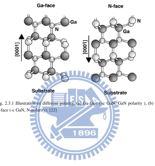
The discrepancy of etching characteristics in Ga-face (+c GaN, Ga-polarity) and
N-face (-c GaN, N-polarity) has been specifically investigated as illustrated in Fig.
2.3.1. Some reports showed that gallium nitride could be etched in the aqueous
sodium hydroxide (NaOH) solution but etching ceased when the formation of an
insoluble coating of presumably gallium hydroxide (Ga(OH)3) [14,15]. For further
etching, it would need removing of the coating by continual jet action. Various
aqueous acid and base solutions have been tested for etching of GaN were list in Table
2.3.1 [16-18]. The undetermined etch rate (nm/min) was because it various from
sample to sample and differences in the defect density. According to the research
reports in recent years; the common cognition related to gallium nitride etching
process was that the most of gallium nitride could be etched rapidly in N-face. The
reason for the face-dependent gallium nitride etching process has been studied by Li
et al., who utilized the X-ray photoelectron spectroscopy (XPS) to examine the
surface chemistries before and after etching process in aqueous KOH solutions for
23
results in Ga- and N-face gallium nitride crystals are due to the different states of
surface bonding. Besides, the most important is the etching process only dependent on
the polarities, not on the surface morphology, growth condition and which atoms form
the surface termination layer. The GaN chemical etching reaction with KOH could be
described as the following formula [19]:
2GaN+3H2OKOH → Ga2O3+2NH3 (2-11) Here, the molten KOH act as a catalyst and a solvent for the resulting Ga2O3 (Fig.
2.3.2 (d)) as well. The mechanism about etching N-face gallium nitride substrate was
illustrated in Fig. 2.3.2. The hydroxide ions (OH-) were first absorbed on the gallium
nitride surface (Fig. 2.3.2 (b)) and finally react with Ga atoms once the OH- ions with
sufficient kinetic energy as shown in the Fig. 2.3.2 (c). The etching could be started at
step (c) if the surface was Ga-terminated. The inertness of Ga-face GaN was ascribed
to the hydroxide ions would be repelled by the negatively-charged triple dangling
bonds of nitrogen near the surface. Thus, if the Ga-face GaN was Ga-terminated, the
etching process stops after the first gallium atom layer was removed. In contrast, for
the N-face GaN, every nitrogen atom bears a single dangling bond to prevent the
24
25
Fig. 2.3.1 Illustration of different polarity, (a) Ga-face (+c GaN, GaN polarity ), (b) N-face (-c GaN, N-polarity). [22]
26
Fig. 2.3.2 Schematic diagrams of the cross section GaN film viewed along [-1-120] direction for N-polar GaN to explain the mechanism of the polarity selective etching. (a) Nitrogen terminated layer with one negatively charged dangling bond on each nitrogen atom; (b) absorption of hydroxide ions; formation of oxides; (d) dissolving the oxides.[23]
27
2.4 Reference
[1] A. Usui, H. Sunakawa, A. Sakai and A. A. Yamaguchi, “Thick GaN epitaxial
growth with low dislocation density by hydride vapor phase epitaxy,” Jpn. J. Appl.
Phys. 36, L889 (1997).
[2] M. Yamada, T. Mitani, Y, Narukawa, S. Shioji, I. Niki, S. Sonobe, K. Deguchi, M.
Sano and T. Mukai, “InGaN-based near-ultraviolet and blue-light-emitting diodes
with high external quantum efficiency using a patterned sapphire substrate and a mesh
electrode,” Jpn. J. Appl. Phys. 41, L1431 (2002).
[3] H. Morkoc¸, S. Strite, G. B. Gao, M. E. Lin, B. Sverdlov, and M. Burns,
“Large‐band‐gap SiC, III‐V nitride, and II‐VI ZnSe‐based semiconductor device
technologies,” J. Appl. Phys. 76, 1363 (1994).
[4] S. Nakamura, T. Mukai, and M. Senoh, “Candela‐class high‐brightness
InGaN/AlGaN double‐heterostructure blue‐light‐emitting diodes,
”
Appl. Phys. Lett.,64, 1687 (1994).
[5] S. D. Lester, F. A. Ponce, M. G. Craford, and D. A. Steigerwald, “High
dislocation densities in high efficiency GaN‐based light‐emitting diodes,” Appl. Phys.
Lett. 66, 1249 (1995).
[6] W. Qian, M. Skowronski, M. DeGraef, K. Doverspike, L. B. Rowland, and D. K.
28
organometallic vapor phase epitaxy,” Appl. Phys. Lett. 66, 1252 (1995).
[7] X. H. Wu, L. M. Brown, D. Kapolnek, S. Keller, B. Keller, S. P. Den-Baars, and J.
S. Speck, “Defect structure of metal‐organic chemical vapor deposition‐grown
epitaxial (0001) GaN/Al2O3,” J. Appl. Phys. 80, 3228 (1996).
[8] B. Garni, J. Ma, N. Perkins, J. Liu, T. F. Kuech, and M. G. Lagally, “Scanning
tunneling microscopy and tunneling luminescence of the surface of GaN films grown
by vapor phase epitaxy,” Appl. Phys. Lett. 68, 1380 (1996).
[9] S. J. Rosner, E. C. Carr, M. J. Ludowise, G. Girolami, and H. I. Erikson,
“Correlation of cathodoluminescence inhomogeneity with microstructural defects in
epitaxial GaN grown by metalorganic chemical-vapor deposition,” Appl. Phys. Lett.
70, 420 (1997).
[10] T. Kozawa, T. Kachi, T. Ohwaki, Y. Taga, N. Koide, and M. Koike, “Dislocation
Etch Pits in GaN Epitaxial Layers Grown on Sapphire Substrates,” J. Electrochem.
Soc. 143, L17 (1996).
[11] S. K. Hong, T. Yao, B. J. Kim, S. Y. Yoon, and T. I. Kim, “Origin of
hexagonal-shaped etch pits formed in (0001) GaN films,” Appl. Phys. Lett. 77, 82
(2000).
[12] S. K. Hong, B. J. Kim, H. S. Park, Y. Park, S. Y. Yoon, and T. I. Kim,
29
etching,” J.Cryst. Growth 191, 275 (1998).
[13] L. Lu, Z. Y. Gao, B. Shen, F. J. Xu, S. Huang, Z. L. Miao, Y. Hao, Z. J. Yang, G.
Y. Zhang, X. P. Zhang, J. Xu, D. P. Yu, “Microstructure and Origin of dislocation
etch pits in GaN epilayers grown by metal organic chemical vapor deposition,” J.
Appl. Phys., 104, 123525 (2008)
[14] T.L. Chu, “Gallium Nitride Films,” J. Electrochem. Soc. 118, 1200 (1971).
[15] J.I. Pankove,” Electrolytic Etching of GaN,” J. Electrochem. Soc. 119, 1118
(1972).
[16] H. Cho, D.C. Hays, C.B. Vartuli, S.J. Pearton, C.R. Abernathy, J.D. MacKenzie,
F. Ren, J.C. Zolper, “Wet chemical etching survey of III-nitrides,” Mater. Res. Soc.
Symp. Proc. 483, 265 (1998).
[17] C.B. Vartuli, S.J. Pearton, C.R. Abernathy, J.D. MacKenzie, F. Ren, J.C. Zolper,
R.J. Shul, “Wet chemical etching survey of III-nitrides,” Solid-State Electron. 41 (12),
1947 (1998).
[18] S.J. Pearton, R.J. Shul, Gallium nitride I, in: J. Pankove, T.D. Moustakas (Eds.),
“The Properties of Hydrogen in GaN and Related Alloys,” Semiconductor and
Semimetals Series, vol. 50, Academic Press, New York, NY, p. 103 (1998).
30
“Selective etching of GaN polar surface in potassium hydroxide solution studied by
x-ray photoelectron spectroscopy,” J. Appl. Phys. 90, 4219 (2001).
[20] D. A. Stocker, E. F. Schubert and J. M. Redwing, “Crystallographic wet chemical
etching of GaN,” Appl. Phys. Lett., Vol. 73, No. 18, 2 November (1998).
[21] M. H. Lo, P. M. Tu, C. H. Wang, C. W. Hung, S. C. Hsu, Y. J. Cheng, H. C. Kuo,
H. W. Zan, S. C. Wang, C. Y. Chang, and S. C. Huang, “High efficiency light emitting
diode with anisotropically etched GaN-sapphire interface,” Appl. Phys. Lett,95
041109 (2009)
[22] O Ambacher, “REVIEW ARTICLE Growth and applications of Group
III-nitrides,” J. Phys. D: Appl. Phys. 31 2653–2710 (1998)
[23] D. S. Li, H. Chen, H. B. Yu, H. Q. Jia, Q. Huang, and J. M. Zhou, “Dependence
of leakage current on dislocations in GaN-based light-emitting diodes,” J. Appl. Phys.,
31
Chapter 3 Measurement System
3.1 Scanning electron microscopy (SEM)
The scanning electron microscope is built of the following parts:
(i) The electron gun
(ii) The system of three-stage electromagnetic lens is used to demagnify (focus,
condense) the electron beam diameter to 5~10 nm at the specimen.
(iii) Detectors may detect electrons, X-ray or cathodo-luminescent (CL) light.
(iv) The microscope column is evacuated to 10-5 torr.
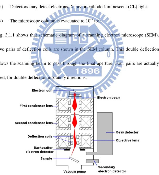
Fig. 3.1.1 shows that schematic diagram of a scanning electron microscope (SEM).
Two pairs of deflection coils are shown in the SEM column. This double deflection
allows the scanning beam to pass through the final aperture. Four pairs are actually
used, for double deflection in x and y directions.
32
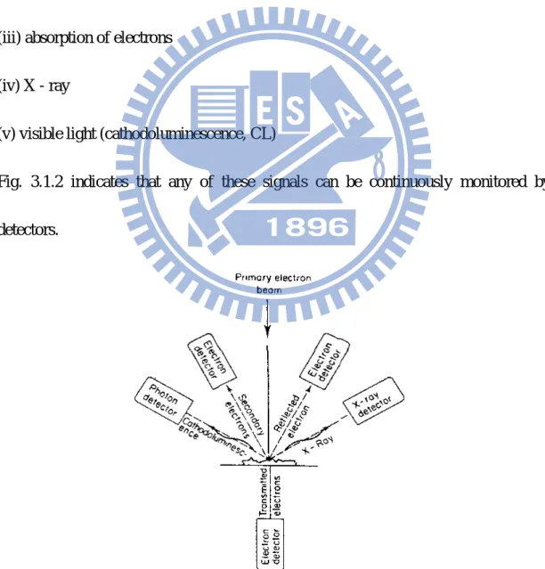
SEM is a technique which forms an image of microscopic region of the specimen
surface. An electron beam from 5~10 nm in diameter is scanned across the specimen.
The interaction of the electron beam with the specimen produces a series of
phenomena such as:
(i) backscattering of electrons of high energy
(ii) secondary electrons of low energy
(iii) absorption of electrons
(iv) X - ray
(v) visible light (cathodoluminescence, CL)
Fig. 3.1.2 indicates that any of these signals can be continuously monitored by
detectors.
33
the sample.[2]
3.2 Cathodoluminescent spectroscopy (CL)
Cathodoluminescence (CL) is a SEM-based technique that can be used for
analyzing the characteristic of semiconductor materials and devices. CL is the
emission of light as the result of electron or “cathode-ray” bombardment. SEM-based
and CL can provide information on the concentration and distribution of luminescent
centers, distribution and density of electrically active defects, and electrical properties
including minority carrier diffusion lengths and lifetimes.
34
3.3 Atomic Force Microscopy (AFM)
Atomic force microscopy (AFM) or scanning force microscopy (SFM) is a very
high-resolution type of scanning probe microscopy (SPM) instead of optical imaging
one. In 1986, the AFM was invented by Gerd Binnig, Christoph Gerber, and Calvin F.
Quate. The AFM is one of the foremost tools for imaging, measuring, and
manipulating matter at the nanoscale. A very tiny, pyramidal probe is attached on the
cantilever. The tip must be very tiny (single atom size) with sharp angle for large-area
scan.
The AFM utilizes a sharp probe moving over the surface of a sample in a raster
scan. When the probe is approaching sample surface, attractive (van der Waals force)
or repulsive force (Coulomb repulsion) between tip and sample is formed and
detected. Forces between the tip and the sample lead to a deflection of the cantilever
according to Hooke's law. The interaction force causes cantilever to shift along z-axis
and thus the topology of sample is obtained. The small probe-sample separation (on
the order of the instrument’s resolution) makes it possible to take measurements over
a small area. To acquire an image the microscope-scans the probe over the sample
while measuring the local property in question. The resulting image resembles an
image on a screen in that both consist of many rows or lines of information placed on
35
lenses, so the size of the probe rather than diffraction effect generally limits their
resolution.
Followings are the operating mode of AFM, shown as the Figs. 3.3[(a)-(c)]:
1. Contact mode: The Interaction mainly comes from repulsive force between tip and
sample. It is easy to obtain atomic-scale resolution, but easy to damage surface of
sample.
2. Non-contact mode: The Interaction mainly comes from van der Waals force
between tip and sample. The tip never touches sample surface; resolution is lower
(~50 nm). The surface of samples is preserved.
3. Tapping mode: The tip touches the surface of samples periodically. The resolution
could be as high as contact-mode. The surface of samples could be damaged
36
(a) (b)
(c)
Fig. 3.3 Operating mode of AFM (a) contact mode, (b) non-contact mode, (c) tapping mode.[2]
3.4 Micro photoluminescence spectroscopy (µ-PL)
Photoluminescence (PL) spectroscopy has been used as a measurement method to
detect the optical properties of the materials because of its nondestructive
characteristics. PL is the emission of light from the material under optical excitation.
Reducing the laser beam spot size to micrometer by beam expanders and objective
lens is the so-called µ-PL. Fig 3.4.1 illustrates the photoluminescence process. The
laser light source used to excite carriers should have large energy band gap than the
semiconductors. When the laser light absorbed within the semiconductors, it should
37
the electrons in the conduction band and the holes in the valance band. When the
electron in an excited state returns to the initial state, it will emit a photon whose
energy is equal to energy difference between the excited state return and the initial
state, therefore, we can observe the emission wavelength peak from PL spectrum.
38
3.5 Reference
[1] http://en.wikipedia.org/wiki/File:Schema_MEB_(en).svg
[2] Class of Materials analysis, S. H. Yang, NCTU in Tainan
39
Chapter 4 Experiment Process
4.1 Experiment Process Flow
First, we reveal the bulk GaN pits of threading dislocation by chemical wet etching.
Second, filling the defect pits by coating silica nanospheres. Finally, regrow UV LED
structure.
In this thesis, we prepare two process samples and a bulk GaN sample as reference.
One of the process sample use molten KOH as etching solution, while the other one
use phosphoric acid. We observe the surface morphology and use optical
measurement to analyze the epitaxial quality.
4.2 GaN surface etching by phosphoric acid and molten KOH
We verified that there are three types of etched pits:screw, edge, mixed(α, β, and γ)type [1]. Each etched pits correspond to different threading dislocations and threading dislocations having a screw component act as strong nonradiative centers
[2], and the different etching liquid may forms different etched pit types. For this
reason, a test round of the two GaN wafer was immersed in molten KOH and
phosphoric acid (H3PO4), respectively.
40
defect density. If the solution temperature or etching time is insufficient, it may lead
to small pit size that is unable to confine the silica nanospheres in the pits. On the
other hand, too much etching time or high solution temperature leads to larger pits
size, which need to re-grow a thicker layer increasing the difficulty to seal the pits.
Moreover, if the GaN is over-etched, the flat area of surface would be too fragile to
provide the platform for re-growth. Therefore, it is important to find an appropriate
recipe for etching process. As shown in fig. 4.2.1, the SEM image of GaN surface
after etching by KOH and H3PO4. In the etching time versus temperature scheme, we
chose 300°C 3 minutes for KOH and 240°C and 4 minutes for H3PO4 etching process.
Both KOH and H3PO4 etching pits size are average about 1.2 um to 1.6 um, and the
pit density is about 107 cm-2 and 106 cm-2 , respectively.
As shown in fig. 4.2.2, three etched pits type are observed. It is known that a screw
type threading dislocation creates a step when it terminates at the GaN surface. In
KOH etching process, these steps are easily attacked by OH-, and further etching
finally stop at the Ga terminate due to the chemical stabilization of Ga face as showed
in fig. 4.2.3 [1]. Finally, the screw type threading dislocations can be etched to an
inverse trapezoid. On the other hand, the edge type etched pits correspond to edge
type threading dislocations. Since every atom in this line has dangling bond, the atom
41
threading dislocations has both screw and edge type morphology.
Fig. 4.2.4 shows the top view SEM image of bulk GaN after etching test. The GaN
etched by KOH revealed three types of etched pits. After calculating the etching pits
density, we found that the edge type pits dominated KOH etching pits, the ratio of
edge type pits is around 85%. On the other hand, We found only screw and mixed
type etched pits in H3PO4 etching sample. The ratio of screw type and mixed type pits
are around 95% and 5%, respectively.
In summary, we could infer that molten KOH prefer to etch edge type dislocation,
while H3PO4 solution prefer to attack screw type dislocation, which is treat as
non-radiative center[2]. In other words H3PO4 solution would much easier reveal
42
(a)
(b)
43
Fig. 4.2.2 The SEM image of GaN wet etching results, three etched pits types are observed.
44
Fig. 4.2.3 [1] (a) Step formed at the beginning of etching screw type threading dislocation. (b) A Ga face to prevent further vertical etching. (c) (d) Edge type threading dislocation was easily etching along the vertical dangling bond line.
(b) (a)
45
(a)
(b)
Fig. 4.2.4 GaN wafer etched by (a)KOH and (b) H3PO4
46
4.3 Coating silica nanospheres on GaN etching surface
We coated diameters 100nm silica nanospheres on GaN surface after revealing
the pits of threading dislocation. The SEM image is shown in fig. 4.3.1. Next step we
removed the silica on the flat surface area and leaves silica nanspheres in the etching
pits. The surface cleaning is the key issue. We wipe off the nanospheres on wafer
surface by dust-free cloth, then clean by ultrasonic vibration in DI water for 5 minutes.
Fig. 4.3.2 shows the difference between our clean process and without using dust-free
cloth. The additional wiping process could totally remove the residual surface
nanospheres.
Fig. 4.3.3 shows the GaN wafer after all cleaning process. We confined the silica
nanospheres in etching pits successfully, and no nanospheres remained on surface.
47
(a) (b)
Fig. 4.3.2 Nanosphere cleaning process with (a) and without (b) dust-free cloth
wiping off the surface.
(a) (b)
Fig.4.3.3 GaN wafer etched by KOHand H3PO4, then spin coating silica nanospheres with diameter 100nm. After cleaning process, the KOH sample (a) and H3PO4 confined the nanospheres successfully.(b)
48
4.4 Regrowth InAlGaN LED structure
The InAlGaN based LED structure were regrown on all samples by using
MOCVD. The LED structure are consisted of a 0.6um u-AlGaN layer, 2.04um
n-InAlGaN layer. Ten pairs of InGaN/InAlGaN multiple quantum well active layer,
29.7nm AlGaN electron blocking layer, and a 55.6 nm p-GaN layer. The LED
structure is showed in Fig. 4.4
The detailed parameters of all samples are shown in table 4.4.
49
Table 4.4 The detail recipe and etching pits density of all process sample
Sample Ref KOH H3PO4
Etching solution - KOH H3PO4
Etching time - 3min 4min
Etching Pits Density(cm-2)
- 1.6x10⁷ 4.25x10⁶
50
4.5 Reference
[1] L. Lu, Z. Y. Gao, B. Shen, F.J.Xu, S.Huang, Z. L. Miao, Y.Hao, Z. J. Yang,
G.Y. Zhang, X. P. Zhang, J. Xu, and D. P. Yu “Microstructure and origin of
dislocation etch pits in GaN epilayers grown by metal organic chemical vapor
deposition,” J. Appl. Phys., 104, 123525 (2008)
[2] T. Hino, S. Tomiya, T. Miyajima, K.Yanashima, S. Hashimoto, and M.Ikeda
“Characterization of threading dislocations in GaN epitaxial layers,” Appl. Phys.
51
Chapter 5 Results and Discussion
5.1 Etching Pits Density analysis
To verify the quality improvement, we etched the p-GaN of LED for etching pits
density (EPD) test again. Fig. 5.1.1 shows SEM image of the etched LED. We observe
that the EPD decrease one order for KOH and two order for H3PO4 sample. This
phenomenon attribute to the success of blocking threading dislocation. The detail
EPD data are shown in table 5.1.
We used SEM observe the LED cross section area. The SEM image for H3PO4 and
KOH is shown in Fig. 5.1.2. We could observe that the propagation of threading
52
Fig. 5.1.1 SEM image of bulk GaN surface and LED surface after EPD test
53
Table 5.1 The EPD data of Bulk GaN and regrow LED surface
5.2 Photoluminescence analysis
Fig. 5.2.1 shows the room temperature PL of the regrow LED. The peak emission
intensity (361nm) of the H3PO4 sample exhibited three times up than the other
sample. We infered that the enhancement could be attributed to fewer defects and
fewer non-radiative centers, which would trap the photo-generated carriers. The
non-radiative center as well as screw type dislocation had been block by silica
nanosphere and led to the strong emission phenomenon.
54
did not exhibit a obvious enhancement. As mention in 4-2, the edge type pits
dominate the KOH etching morphology, which is not non-radiative center.
We fitted the power dependent PL spectrum, and the H3PO4 sample exhibits a
55
Fig. 5.2.1 Photoluminescence spectrum of DSP LED
Fig 5.2.2 Power Dependent PL Fitting of DSP LED
320340360 380400420440460 480500520
-2000 0 2000 4000 6000 8000 10000 12000 14000Inte
ns
ity
(a.
u
)
Wavelength(nm) H3PO4 KOH Ref0
2000 4000 6000 8000 10000
0
5000
10000
15000
20000
25000
30000
35000
H3PO4 KOH RefP
e
ak
Inte
ns
ity
(a.
u
)
Pumping Power(uw)
56
5.3 Cathodoluminescence analysis
The optical characteristic is investigated by SEM and cathodoluminescence(CL)
images as shown in Fig. 5.3.1. The image was taken under the quantum well emission
wavelength as well as 361nm. The results implied the H3PO4 sample exhibited larger
and more uniform luminescence area, which is showed less non-radiative center. We
could infer that the material quality of H3PO4 sample has been improved. However,
the KOH sample quality was decreased for some reason. The decrease may due to the
epitaxial process problem.
We also analyze the CL spectrum under full wavelength with PMT 750 volt. The
intensity trend was in agreement with PL measurement. The results showed in Fig.
57
Figs. 5.3.1 CL measurement of DSP LED and Reference under quantum wavelength
Fig. 5.3.2 CL measurement of DSP LED and Reference under full wavelength
320340360380400420440460480500520
0
20000
40000
60000
80000
100000
120000
Int
e
nsi
ty(
cn
t)
Wavelength(nm)
H3PO4 KOH Ref58
5.4 Internal quantum efficiency
We calculated the internal quantum efficiency (IQE) by liquid Helium cooling
system. We set 20K as IQE 100% point and compared to room temperature. We found the IQE for H3PO4 , KOH and reference sample is 15.7% , 3.7% and 13.4%, respectively. Fig 5.4.1 shows the IQE results. The H3PO4 has been improved, but the KOH sample decreased. The KOH sample may have some epitaxial problem in quantum well.
Fig. 5.4.1 The IQE results of LEDs
0
10
20
30
40
50
0.0
0.2
0.4
0.6
0.8
1.0
H3PO4 KOH RefN
or
m
a
li
ze
d P
L I
nt
e
nsi
ty
(a
.u)
1000/T (K
-1)
59
5.5 Reflection analysis
Fig. 5.5.1 shows the reflection of all LEDs. The reflection of H3PO4 and KOH sample are 2.6% and 2.1% higher than reference in wavelength 361nm. We verified the possibility that using silica nanopheres act as reflector in ultraviolet LED.
Fig. 5.5.2 shows the absorption of all LEDs. The absorption of H3PO4, KOH, and
60
Fig. 5.5.1 Reflection of silica nanospheres embedded LED
Fig. 5.5.2 Absorption of silica nanospheres embedded LED
300
400
500
600
700
800
0
20
40
60
80
100
A
bso
rpt
ion (
%
)
Wavelength (nm)
H3PO4 KOH Reference61
Chapter 6 Conclusion
We simplified the defect passivation process (DSP), replacing PECVD and
CMP process by embedding silica nanospheres. The DSP using silica nanospheres
blocking the quantum well penetration of threading dislocation is much cheaper and
convenience.
Furthermore, we confirmed that the H3PO4 prefer to etch screw type dislocation,
which is treated as non-radiative centers. On the other hand, KOH prefer to attack
edge type dislocation, which is considered no relation with non-radiative center.
Finally, the reflection estimation exhibits a 2% enhancement in ultraviolet
wavelength (361nm) compared to reference sample, which means we could use silica


![Fig. 2.1.2 Radiative and non-radiative recombination in active region. [21]](https://thumb-ap.123doks.com/thumbv2/9libinfo/8409567.179765/27.892.147.754.458.943/fig-radiative-non-radiative-recombination-active-region.webp)
![Fig. 2.1.4 Total internal reflection in GaN-based LED. [21]](https://thumb-ap.123doks.com/thumbv2/9libinfo/8409567.179765/28.892.274.619.455.920/fig-total-internal-reflection-gan-based-led.webp)
![Fig. 2.1.5 The angle of total internal reflection defines the light-escape cone. [21]](https://thumb-ap.123doks.com/thumbv2/9libinfo/8409567.179765/29.892.137.744.133.801/fig-angle-total-internal-reflection-defines-light-escape.webp)
![Table 2.3 Various chemicals etch GaN.[20]](https://thumb-ap.123doks.com/thumbv2/9libinfo/8409567.179765/35.892.204.684.219.817/table-various-chemicals-etch-gan.webp)
![Fig. 2.3.2 Schematic diagrams of the cross section GaN film viewed along [-1-120] direction for N-polar GaN to explain the mechanism of the polarity selective etching](https://thumb-ap.123doks.com/thumbv2/9libinfo/8409567.179765/37.892.190.697.126.947/schematic-diagrams-direction-explain-mechanism-polarity-selective-etching.webp)