行政院國家科學委員會專題研究計畫
期末進度報告
強關聯量子物質之材料、界面、與其衍生性物理
特 性 研 究
-子 計 畫 四 :強 關 聯 量 子 材 料 及 結 構 之 相
分離研究
(3/3)
計畫 別: 整合型 計畫編號: NSC 98-2112-M-009-007-MY3 執 期間: 2009 年 08 月 01 日至 2013 年 01 月 31日 執行單位: 國立交通大學電子物 學系(所) 計畫主持人: 溫增明 處理方式: 期末報告不提供公開查詢 中 華 民 國 102 年 03 月15 日行政院國家科學委員會補助專題研究
計畫
(計畫名稱)
強關聯量子物質之材料、界面、與其衍生性物理
特 性 研 究
-子 計 畫 四 :強 關 聯 量 子 材 料 及 結 構 之 相
分離研究
(3/3)
計畫類別:
□個別型計畫 □整合型計畫
計畫編號:
NSC
98-2112-M-009-007-MY3
執行期間:
2009 年 08 月 01 日至 2013 年 01 月 31 日
執行機構及系所:國
交通大學電子物
學系(所)
計畫主持人:溫增明 共同主持人:莊振益 計畫參與人員:郭 韋 呈 、 宓 君 緯 、 蔡 婷 、 江 堯 薇 、 賴 軍 佑 、 宗 漢 、 王 家彬 成果報告類型(依經費核定清單規定繳交):□精簡報告 □完整報告 本計畫除繳交成果報告外,另須繳交以下出國心得報告: □赴國外出差或研習心得報告 □赴大陸地區出差或研習心得報告 □出席國際學術會議心得報告 □國際合作研究計畫國外研究報告 執 單位:交通大學 電子物 系 中 華 民 國 102 03 月 15 日計畫中文摘要
在近幾年的研究中,在低溫下的鉍錳氧(BMO)鈣鈦礦結構已被證
實具有多鐵的性質。本實驗中我們利用脈衝雷射濺鍍膜系統在鋁酸
鑭
(LAO)基板上磊晶出鉍和錳的氧化物薄膜。接著利用高解析度
X-Ray 繞射儀確認薄膜的晶體結構、利用吸收光譜(XAS)探測在薄膜中
錳的電子價態、電子穿遂顯微鏡
(TEM)觀測晶格結構、在用壓電力
顯微鏡(PFM)量測鐵電特性以及用超導量子干涉儀(SQUID)了解磁性。
經由以上實驗我們發現成長在鋁酸鑭上的鉍錳氧薄膜同時存在鐵磁
以及鐵電的特性,而後我們將薄膜應用在電阻式記憶體元件,且得
到良好的成果,這項結果使得我們有興趣繼續對此薄膜做進一步的
探討以便瞭解磁電耦合和記憶體元件裡電阻轉態的機制是如何發生
在此薄膜系統裡。
Abstract
Multiferroic materials, which possess coupled electric, magnetic and structural order parameters in the same phase, have attracted considerable attention among strong-correlated complex oxide systems. These materials are not only interesting from a scientific point of view but also promising in novel application possibilities. In previous study, low temperature multiferroic properties in perovskite type BiMnO3 (BMO) has been demonstrated. In this work, through epitaxial strains exerted by LaAlO3 single crystal substrate, we demonstrated the growth of the several possible structures as Mn2O3, MnO2, Bi2O3, …etc, combined within the same thin film. We further revealed manganese valence through the X-ray Absorption Spectroscopy (XAS) measurement and exhibit the mixed +3 and +4 valence of manganese. With LaNiO3 bottom electrode, room-temperature ferroelectricity is demonstrated by Piezoelectric Force Microscopy (PFM). Magnetization-magnetic field curves measured by SQUID magnetometer as a function of temperatures. Ferromagnetic behaviors have been probed from room temperature (300 K) to low temperature (10 K), furthermore, 5 emu/cc of saturation magnetization at 300 K has been observed. In our preliminary results, room temperature ferroelectric and ferromagnetic properties could be coexistent in our material. The outstanding properties of application with resistive random-access memory device have been demonstrated by the resistive switching behavior.
I.
Introduction
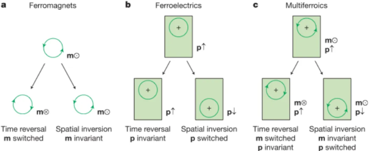
In certainly many scientists have been hardly investigated the magnetic and electric materials and found several the interesting phenomenon such as multiferroic1 property in the thin film or superlattice and further permeate every aspect of modern technology. From the investigation of bulk single crystals to novel characterization techniques that probe order parameters, coupling, and spin dynamics this is truly a diverse field, rich with experimental and theoretical complexity. By definition, a single-phase multiferroic is a material that simultaneously possesses two or more of the so-called ‘‘ferroic’’ order parameters-ferroelectricity, ferromagnetism, and ferroelasticity. The overlap required of ferroic (Fig. 1) materials to be classified as multiferroic is shown schematically in Fig. 2(a). The electricfield E, magnetic field H, and stress σ control the electric polarization P, magnetization M, and strain ε, respectively. In a ferroic material, P, M, or ε are spontaneously formed to produce ferromagnetism, ferroelectricity, or ferroelasticity, respectively. In a multiferroic, the coexistence of at least two ferroic forms of ordering leads to additional interactions. In a magnetoelectric multiferroic, a magnetic field may control P or an electric field may control M (green arrows).( Fig. 2 (b))
Fig. 1. Time-reversal and spatial-inversion symmetry in ferroics. (a) Ferromagnets. The local magnetic
moment m may be represented classically by a charge that dynamically traces an orbit, as indicated by the arrowheads. A spatial inversion produces no change, but time reversal switches the orbit and thus m. (b) Ferroelectrics. The local dipole moment p may be represented by a positive point charge that lies asymmetrically within a crystallographic unit cell that has no net charge. There is no net time
dependence, but spatial inversion reverses p. (c) Multiferroics that are both ferromagnetic and ferroelectric possess neither symmetry. (Adapted from Ref. [2])
Fig. 2. (a) The relationship between multiferroic and magnetoelectric materials. Ferromagnets
(ferroelectrics) form a subset of magnetically (electrically) polarizable materials such as paramagnets and antiferromagnets (paraelectrics and antiferroelectrics). The intersection (red hatching) represents materials that are multiferroic. Magnetoelectric coupling (blue hatching) is an independent phenomenon that can, but need not, arise in any of the materials that are both magnetically and electrically polarizable. In practice, it is likely to arise in all such materials, either directly or via strain.
(Adapted from Ref. [2].) (b) Schematic illustrating different types of coupling present in materials. Much attention has been given to materials where electric and magnetic order is coupled. These materials are known as magnetoelectric materials. (Adapted from Ref. [3].)
A confluence of three factors explains the current high level of interest in magnetoelectrics and multiferroics. First, in 2000, Hill (now Spaldin) discussed the conditions required for ferroelectricity and ferromagnetism to be compatible in oxides,
and declared them to be rarely met4. Her paper in effect issued a grand materials
development challenge that was taken up because empirically there are indeed few multiferroic materials, whatever the microscopic reasons. Second, the experimental machinery for the synthesis and study of various contenders was already in place when this happened. Third, the relentless drive towards ever better technology is aided by the study of novel materials. Aspirations here include transducers and magnetic field sensors, but tend to centre on the information storage industry.
It was initially suggested that both magnetization and polarization could independently encode information in a single multiferroic bit. Four-state memory has
recently been demonstrated5, but in practice it is likely that the two order parameters
are coupled6,7. Coupling could in principle permit data to be written electrically and
read magnetically. This is attractive, given that it would exploit the best aspects of ferroelectric random access memory (FeRAM) and magnetic data storage, while avoiding the problems associated with reading FeRAM and generating the large local magnetic fields needed to write. Unfortunately, significant materials developments will be required to generate magnetoelectric materials that could make a real contribution to the data storage industry. But given the paucity of serious competitors to contemporary memory technologies, the study of novel materials remains important if disruptive technologies are ultimately to emerge.
Recently, a resistive random-access memory have been reported and such a
resistance switch was described in ferroelectric ZnxCd1−xS. many related memory concepts have been described that employ insulator-metal or metal-semiconductor-metal structures to switch the conduction state under voltage bias in a reversible manner that changes the electrical resistance by several orders of magnitude8-14. In our case, the resistive switching properties of Pt/(Bi, Mn)O/Pt structure and displayed a fine result in the typical I-V characteristics measured with two operation modes in resistance switching that will be reported in later section. Magnetoelectric properties exist the magnetic various coupled with a applied electric field and electric various coupled with a applied magnetic field. The manganite complex oxides has configuration of valence structures between neighbor manganite cause the orbital interaction to determine the magnetic properties. The electric behavior of Mn-O-Mn interaction always determine the magnetic structures like the rare-earth manganite. As for room-temperature crystal structure and dielectric property, BiMnO3 is monoclinic and ferroelectric:15,16 in contrast, light rare-earth
manganites ReMnO3 (Re = La–Dy) are orthorhombic and nonferroelectric, whereas,
the heavy ones ReMnO3 (Re = Y, Ho–Lu) are hexagonal and ferroelectric. The
ReMnO3 even exist the antiferromagnetic and colossal magnetoresistance (CMR)
properties. It is noteworthy here that Bi3+ and Re3+ ions are very similar both in valence state and ionic radius.The electronic configuration of Mn3+ ion in BiMnO
3 is
𝑡!!! 𝑒
!! (spin quantum number S=2) as in a famous orbital-ordered manganite LaMnO3.
The ionic radius of Bi3+ (1.24 Å in nine-coordination) on an A-site is very close to that of La3+ (1.22 Å)17. However, BiMnO3 shows the ferromagnetism below ~105 K18,19 in
properties, BiMnO3 is an insulator un-like double-exchange ferromagnets such as
(La,Sr)MnO3. Furthermore, a ferroelectric hysteresis loop has been reported in the
ferromagnetic state of impure samples recently20. The detailed crystal structure of BiMnO3 with the 6s2 lone pair in Bi3+ is monoclinic (space group; C2)21, which
indicates that the system has an off-center distortion responsible for the polar behavior.
The remarkable magnetoelectric properties of BiMnO3 have attracted considerable
attention during the last three years. It is well established that BiMnO3 becomes
ferromagnetically ordered on cooling below 110 K,22-24 and there is good reason to
believe that the ferromagnetism coexists with ferroelectricity. As the recent paper reported25 that the ferromagnetic structure of BiMnO3 is a distorted perovskite that
crystallizes in the monoclinic space group C2 with unit-cell parameters a=9.5317(7) Å, b=5.6047(4) Å, c=9.8492(7) Å, and ß=110.60(1)°. There is no crystallographic phase transition on cooling the polar room-temperature structure to 20 K, lending support to the belief that ferromagnetism and ferroelectricity coexist in BiMnO3.
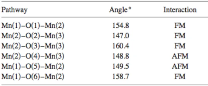
Careful examination of the six unique Mn-O-Mn superexchange pathways between the three crystallographically independent Mn3+ sites shows that four are ferromagnetic and two are antiferromagnetic, thereby confirming that the ferromagnetism of BiMnO3 stems directly from orbital ordering. The coordination
environments for the Bi and Mn atoms are shown in Figs. 3 and 4,25 respectively. The BiOn polyhedra are unsymmetrical as a consequence of the stereochemical activity of
the lone pairs of electrons on the Bi3+ ions. This asymmetry is believed to be the major driving force behind the ferroelectric properties of BiMnO3, as it is in the
behavior of Pb(ZrxTi1-x)O3 (PZT) and related phases. In both BiMnO3 and PZT for
example, the A cations are displaced approximately along the body diagonal of the cubic perovskite subcell. The fact that there is no structural phase transition and that the distortions remain substantially the same on cooling from room temperature to 20 K lends strong support to the belief that BiMnO3 remains ferroelectric in the
ferromagnetic phase.
FIG. 3. Coordination environments of Bi1 and Bi2; showing
the shortest distances in bold and longer ones in dashed lines.
FIG. 4. Coordination environment of the Jahn-Teller distorted Mn cations.
FIG. 5. Three-dimentional magnetic exchange
between the Mn atoms; the thick lines correspond to theoccupied 𝑑!! orbitals.
TABLE I. Primary superexchange interactions in BiMnO3 at 20 K. The bond angle estimated standard deviations are ~0.3°.
Each of the three MnO6 polyhedra shows the axial elongation that is typical of
Jahn-Teller distorted d4 cations in perovskite systems. The orbital ordering that is associated with these distortions in BiMnO3 is the same as that observed at room
temperature (shown as Fig. 5),25 resulting in super-exchange interactions that are largely ferromagnetic (see in Table I).25 In four of the six pathways, the orbital ordering ensures that half filled 𝑑!! orbitals point towards the empty 𝑑!!!!! orbitals
on the next manganese; such interactions are predicted to be ferromagnetic according to the rules proposed by Goodenough26,27 and Kanamori;28 they are strongest when the M-O-M bond angle is close to 180°. We note that three of the four ferromagnetic Mn-O-Mn angles are significantly larger than the antiferromagnetic ones (Table I). There is no instance in which a half filled 𝑑!! orbital points towards another half
filled 𝑑!! orbital, but two cases in which empty 𝑑!!!!! orbitals point towards each
other [through O(4) and O(5)]. Optimally, these interactions would be weakly antiferromagnetic, but this cannot be accommodated in combination with the constraints of the strong ferromagnetic interactions, so the system must be slightly frustrated.
Besides the multiferroic properties of powder structure of BMO, there have another form of BMO to research multiferrioc properties is that established the thin film. As the recent reported29 in 2005, BiMnO3 (010) films (100 nm) were grown
epitaxially on SrTiO3 (001) and 0.2 at. % Nb-doped SrTiO3 (001) substrates using
pulsed laser deposition. The microstructure, electrical, and magnetic properties, and indeed the formation of the correct phase, were found to be very sensitive to growth
parameters. Figures 6(a)–6(d) show AFM images and full width half maxima
(FWHM) of the BMO (010) reflection for BMO films grown at a substrate
temperature30 (Ts) of 450 °C and 0.1 Pa O2 using laser fluences in the range from 1.1
to 2.2 J/cm2. Figure 6(e) shows the magnetization curves for these films at 15 K. A
laser fluence of 1.5 J/cm2 resulted in the lowest surface roughness (scale bar =7 nm,
root-mean-square roughness = 0.5 nm) and largest Ms of 2.2 µB/Mn. This film also
had the largest TC of about 85 K (TC bulk=105 K). Small deviations from this fluence
resulted in an increase of the surface roughness and a decrease of Ms and TC. The
small FWHM indicates good alignment between the film and the substrate.
Using optimal laser fluence of 1.5 J/cm2, the pressure of the flowing oxygen
ambient during growth was varied from run to run in the range of 0.03–0.3 Pa. The narrowest rocking curve and smoothest surface were obtained at 0.1 Pa. Films grown
with 0.1 Pa and 0.3 Pa had the same Ms of 2.2 µB/Mn. On the other hand, when BMO
was deposited in a flowing ambient of 0.03 Pa O2 or 10 Pa Ar, no peaks in XRD or
ferromagnetism could be detected. Similarly, Ts was varied from run to run between
370 and 530 °C. The smoothest surface, smallest FWHM, and largest Ms were
obtained at Ts=450 °C as shown previously in Fig. 6(c). Small changes in temperature
result either in increased surface roughness [Fig. 7(b)] or reduced Ms [Fig. 7(c)]. No
BMO peaks were observed with XRD for films grown at 370 or 530 °C, which suggests that 400 and 500 °C are approximate lower and upper bounds for BMO growth.
FIG. 6. AFM images of 2×2 µm2 regions of 100 nm BMO films grown at 450 °C and 0.1 Pa O 2 with a
each image states the FWHM of the BMO (010) rocking curve. The surface roughnesses are indicated by the scalebars. (e) Magnetization loops obtained at 15 K.
Besides the standard anneal at 370 °C with pO2 = 0.1 Pa, films grown at Ts =410 °
C (prior to establishing the optimal value of Ts =450 °C) were also cooled
immediately after deposition without annealing or annealed in a high oxygen pressure of 50 kPa. In fact, a non-annealed film had the same FWHM and Ms of 1.2 µB/Mn as a standard annealed film, but annealing in the high oxygen pressure significantly
reduced both the intensity of the BMO peak and Ms to 0.12 µB/Mn. This ten-fold
reduction in magnetization has also been observed in bulk ceramic BMO annealed in
air at 500 °C for 4 h.31 As different multiferroic properties consist of bulk and thin
film of BMO displayed the complex magnetoelectric coupling effect lead us have interested to investigate these phenomenon in this system.
FIG. 7. AFM images of 2×2 µm2 regions of 100 nm BMO films grown at a laser fluence of 1.5 J/cm2
using a growth temperature Ts of (a) 400 °C and (b) 500 °C. (c) Magnetization loops taken at 15 K for
BMO films grown at 400, 450, and 500 °C.
II. Result & discussion
a. Analysis of bismuth manganite thin film structure
Bismuth-containing perovskites have attracted much attention as multiferroic and lead-free ferroelectric materials.32-36 Among the multiferroic properties in bismuth manganite complex oxide let we have interested in physical properties of magnetoelectric coupling effect in bismuth manganite thin films. In order to demonstrate our experiment, we deposited the bismuth manganite oxide thin film by means of pulse laser deposition system.
The XRD diffraction patterns of our bismuth manganite powder had been fitted as result revealed the possible structures as Bi2Mn4O10, Bi2MnO20 or Bi2O3 [see in Fig. 8(a)]. In figures 8(b)~(f), we deposited bismuth manganite on different substrates such as LaAlO3, SrTiO3, YAlO3, DyScO3 and NdGaO3 with different growth temperature. In fig. 8(b), we tried to grow BMO on NGO substrate dependence of temperature from 400 °C to 800 °C and have no any crystalline structure on the NGO with all range of growth temperatures besides for 500 °C and 600 °C. As result of the X-ray diffraction pattern from 600 °C sample we compared with previous research
paper37-42 and supposed us to believe that BMO deposited alone a-axis oriented on
NGO. In fig. 8(c), the best condition for DSO substrate seems to 500 °C. Fig. 8(d) show the crystalline growth on YAO among 500 °C and 600 °C and we especially took a look for these two XRD patterns detail separately with determination of d-spacing in BMO thin films. The situation in 600 °C we calculated three peaks near by (110) oriented of NGO and correspond with multiple relations lead us to suppose that BMO grown as one kind of lattice direction on NGO substrate. In Fig. 8(e) there is almost no peak in XRD diffraction patterns with a series of temperature consist with STO substrate. The final comparable substrate, we grown on LAO at different temperature from 400 °C to 550 °C and demonstrated the stable parameters at 500 °C. After all, we demonstrated all substrate but only LAO displayed the repeatable result of crystalline growth.
(b) (c) (d) (e) (f) (a)
FIG. 8. (a) Fitting curves of bismuth manganite. High Resolution X-Ray diffraction patterns measured dependent on different substrates with a sequence of several temperatures dependence of (b) show the BMO deposited on NGO substrate, (c) DSO substrate, (d) YAO substrate, and (e) STO substrate with different temperatures from 400 °C to 800 °C. (f) LAO substrate as different temperature from 400 °C to 550 °C.
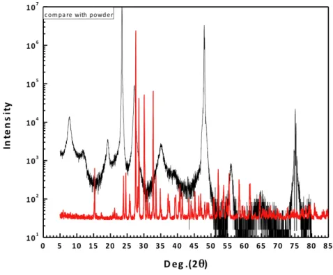
As result of the XRD diffraction patterns of bismuth manganite thin film compared with powder as Fig. 9. revealed that structure of thin film different from powder which lead us to compare with data base from software of PCPDFWIN. As the
comparison, we obtained several possible compounds such as Mn2O3, MnO2, Bi2O3, etc (In Table II). After then, we defined our bismuth manganite thin film named as (Bi, Mn)Ox and the X-Ray diffraction patterns of (Bi, Mn)Ox thin film on LAO substrate
at room temperature shown in figure 10(a). All positions of peak for (Bi, Mn)Ox have
been remarked as those possible bismuth oxide and manganite consist of each orientation of plane indicated by Miller index. We compared with another XRD patterns of BiMnO/LaAlO3 [inset of Fig. 10(a)] deposited with sputtering system by
department of Materials Science and Engineering University of Berkeley, but there is no peak coincide on the same position of XRD patterns under result of comparison. We keep trying to compare with other reference papers and had a same result.
Fig. 9. The (Bi, Mn)Ox thin film compared with bismuth manganite powder presented by X-Ray diffraction patterns.
The surface topography of the surface and growth conditions strongly influences the quality of the grown films. The surface topographies of the thin film, with scan resolutions of 5 x 5 µm2 [shown as figure 10(b)] by using AFM tapping mode scan and display the uniform and smooth surface in (Bi, Mn)Ox thin film. Furthermore, the
thin film morphology on a wide range of scan lengths 5 µm corresponding with the white line in figure 10(b) was scanned as result of figure 10(c). The figure presents the Z-X curve to show that the roughness is about 0.369 nm (Ra) by functional calculations build inside of AFM instrument. This result suppose us to realize that roughness of (Bi, Mn)Ox thin film approach to the lattice constant of LAO substrate.
To understand this XRD pattern of (Bi, Mn)Ox thin film, we calculated d-spacing of
each novel peak and got result to show that each of pattern have no multiple relations compared with all (Bi, Mn)Ox peaks, lending support to belief that components of our
thin film structure combined with several kinds of single crystal structures. In recent work, we keep pushing on measurement of TEM/EDS instrument to realize high resolution lattice structure of (Bi, Mn)Ox thin film to identify that what space group
(Bi, Mn)Ox does in our case, and determined lattice constant along the a, b, c-axis.
FIG. 10. (a) Room temperature X-Ray diffraction pattern of (Bi, Mn)Ox on LAO, (b) the top view of
thin film grown on LAO topography scanned by means of atomic force microscopy, (c) cross-section view of the (Bi, Mn)Ox film dependent on the white line in figure (b).
b. Electric properties
Electric properties of the ferroelectric domain structure of (Bi, Mn)Ox thin films
can be determined and characterized by piezoelectric force microscopy (PFM)43~45. In
this technique, a conductive cantilever with an ac signal induces an alternating
electrical field between the tip and the LaNiO3 (LNO) bottom electrode. Local
converse piezoelectric vibrations induced by the ac field produce displacements of the film. Using a lock-in technique enables the detection and recording of the sign and phase of the piezoelectric vibration, which can be used in conjunction with crystallographic information to determine the polarization direction in the films. Domains with up- and down-polarizations give rise to opposite contrast in out-of-plane (OP)-PFM images and differences in in-out-of-plane components of polarization produce a torque on the atomic force microscope (AFM) cantilever creating contrast in the in-plane (IP)-PFM images. However, domains with polarization vectors along the scanning cantilever’s long axis do not give rise to any IP-PFM contrast. On the contrary, domains with polarization pointing to the right with respect to the cantilever’s long axis produce an opposite tone to domains with a polarization pointing to the left. This is caused by the antiphase IP-piezoresponse (PR) signals produced by these domains. By combining the OP- and IP-PFM images, therefore, we can identify the polarization direction of each domain.
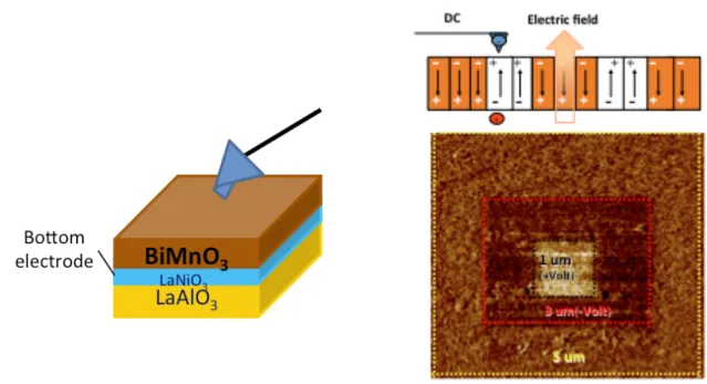
Electrical control of ferroelectric behavior in (Bi, Mn)Ox thin films relies on
controlling the ferroelectric switching. To switch the films locally, a dc bias is applied
to a conducting AFM tip while scanning over the desired area. In figure 10, 5×5 µm2
region have no any dc bias and following step we applied a dc bias during the region
3×3 µm2 build by red dotted line and last applied a opposite dc bias in area 1×1 µm2.
From 5×5 µm2 region presents the random direction of polarization and in the
following step through the vertical dc bias in (Bi, Mn)Ox surface display the deep
bias correspond with up-polarization and in the last region 1×1 µm2 applied the opposite dc bias caused the light color than outside dependent on down-polarization. Through the PFM scan, we identified the ferroelectric properties of (Bi, Mn)Ox thin
film and the next step of measurement is determinate value of polarization in (Bi, Mn)Ox ferroelectric domain probe by PFM in cooperation school named National
Cheng Kung University.
FIG. 11. The phase diagram scanned by means of piezoelectric force microscopy dependence on applied dc bias as different direction consist with different regions.
c. Magnetic properties
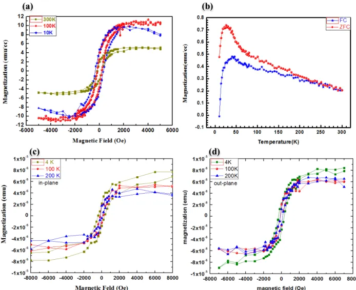
On figure 12(a), we plot the magnetization (M) vs applied magnetic field (H)
perpendicular to c-axis oriented of LAO substrate for a 80-nm-thick (Bi, Mn)Ox film
with a sequence of three kinds of different temperatures for 10 K, 100 K, and 300 K after subtracting the diamagnetic contribution of the LAO substrate. We observe a
clear ferromagnetic behavior with a coercive field of 200 Oe measured in at 100 K
similar to 300 K, 300 Oe at 10 K, and a remanence of 2.07 emu/cm3 at 300 K, 4.11
emu/cm3 at 100 K, 4.73 emu/cm3 at 10 K, respectively. The shape of the
magnetization loops indicates that the easy axis clearly lies in ab-plane and c-plane compared with result of out-plane [Fig. 12(d)] of LAO substrate. The saturation
magnetization compared with 10 K, 100 K, and 300 K is approach to 10 emu/cm3 at
1200 Oe similar to 100 K, and 5 emu/cm3 at 2000 Oe. We can easily see that 10 K
and 100 K have the same value of saturation magnetization supported us to speculate that variation of spin structure among this range of temperature is greatly small until to 300 K. As demonstrated in figure 12(b), magnetization dependent on temperature curve has been measured with FC and ZFC curves at an applied magnetic field of 300 Oe.
The separation of difference was observed between the ZFC and FC curves below
about 260 K with no difference above this temperature. The first transition temperature is about 65 K and the second transition temperature is about 30 K. From
this result, we supported that our (Bi, Mn)Ox thin film have last two kinds of single
crystal combined with each other caused by the antiferromagnetic behavior appear from 260 K to 65 K and coupled with tendency towards ferromagnetic from 65 K, this result caused the non-symmetrical magnetic hysteresis loop. Figure 12(c) and (d) display the M-H hysteresis loop with different applied magnetic field perpendicular and parallel to (100) orientation of LAO. The saturation magnetization of the out-plane applied H is bigger than in-out-plane ones.
(a) (b)
(c) (d)
FIG. 12. (a) magnetization hysteresis cycles measured at different temperature 10 K, 100 K, 300 K with the magnetic field applied perpendicular to c-axis oriented of LAO, (b) Magnetization dependence of temperature from 10 K to 300 K in the applied magnetic field of 300 Oe, (c) and (d) show the M-H curves with different direction of apply magnetic field in- and out-plane dependence of 4 K, 100 K and 200 K, respectively.
In the further experiments, we employed as a systematic x-ray absorption spectroscopy (XAS) in NSRRC study of valence state of magnesium in (Bi, Mn)Ox
thin films. Figure 13(a), shows the Mn TEY XAS spectra and their comparison with the reference data46 of Mn2+ (MnO), Mn3+ (LaMnO3), and Mn4+ (EuCo0.5Mn0.5O3 and
SrMnO3)from Ref [47]. Similar PFY spectra, although slightly distorted by saturation
effects in fluorescence-yield modes,47 were obtained as shown in Fig. 13(b), which shows that our spectra come from (Bi, Mn)Ox intrinsic electronic structures shown the
Mn L2,3-edges XAS spectra at room temperature. We can clearly saw that the Mn L3
-edge built of three peaks similar to combination curve of Mn4+ (EuCo0.5Mn0.5O3) and
Mn3+ (LaMnO
3) curves compared with reference XAS data.
This figure indicated that there have two valence states of Mn3+ and Mn4+ mixed
structure in our (Bi, Mn)Ox thin film relies on different lattice structures combined
together in thin film. From this result, we speculated that mixed spin structure of Mn3+ and Mn4+ valence state caused ferromagnetism and antiferromagnetism behavior coupled in one (Bi, Mn)Ox thin film correspond with magnetic measurement
like magnetization dependence of applied magnetic field and magnetization dependence of temperature we have reported and this suggestion needs more experiments to identify it relies on TEM measurement to realize the lattice structure and XMLD, XMCD to know the information of magnetic properties in the (Bi, Mn)Ox thin films.
FIG. 13. (a) Mn 2p XAS spectra and their comparison with the reference data of Mn2+ (MnO), Mn3+(LaMnO
3), and Mn4+ (EuCo0.5Mn0.5O3 and SrMnO3) from Ref [47], (b) Mn L2,3-edges of TEY
XAS spectra measured at 300 K in National Synchrotron Radiation Research Center in Taiwan.
d. Application of RRAM
Resistive random-access memory (RRAM) is a new non-volatile memory type
being developed by many companies. The technology bears some similarities to CBRAM and phase change memory. Different forms of RRAM have been disclosed, based on different dielectric materials, spanning from perovskites to transition metal oxides to chalcogenides. Even silicon dioxide has been shown to exhibit resistive switching as early as 1967,48 and has recently been revisited.49The basic idea is that a dielectric, which is normally insulating, can be made to conduct through a filament or conduction path formed after application of a sufficiently high voltage. The conduction path formation can arise from different mechanisms, including defects, metal migration, etc. Once the filament is formed, it may be reset (broken, resulting in high resistance) or set (re-formed, resulting in lower resistance) by an appropriately applied voltage. Recent data suggest that many current paths, rather than a single filament, are probably involved.50
A memory cell can be deduced from the basic memory cell in three different ways. In the simplest approach, the pure memory element can be used as a basic memory cell, resulting in a configuration where parallel bitlines are crossed by perpendicular wordlines with the switching material placed between wordline and bitline at every cross-point. This configuration is called a cross-point cell. Since this architecture will lead to a large parasitic current flowing through non selected memory cells, the cross-point array has a very slow read access. A selection element can be added to improve the situation. A series connection of a diode in every cross-point allows to reverse bias all non selected cells. This can be arranged in a similar compact manner as the basic cross-point cell. Finally a transistor device (ideally a MOS Transistor) can be added which makes the selection of a cell very easy and therefore gives the best random access time, but comes at the price of increased area consumption.
For random access type memories, a transistor type architecture is preferred while the cross-point architecture and the diode architecture open the path toward stacking memory layers on top of each other and therefore are ideally suited for mass storage devices. The switching mechanism itself can be classified in different dimensions. First there are effects where the polarity between switching from the low to the high resistance level (set operation) is reversed compared to the switching between the high and the low resistance level (reset operation). These effects are called bipolar switching effects. On the contrary, there are also unipolar switching effects where both, set and reset operation, require the same polarity, but different voltage magnitude.
Another way to distinguish switching effects is based on the localization of the low resistive path. Many resistive switching effects show a filamentary behavior, where only one or a few very narrow low resistive paths exist in the low resistive state. In contrast, also homogenous switching of the whole area can be observed. Both effects can occur either throughout the entire distance between the electrodes or happen only in close proximity to one of the electrodes. Filamentary and homogenous switching effects can be distinguished by measuring the area dependence of the low resistance state.
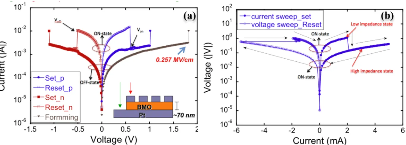
Typical dc current-voltage (I-V) characteristics from Pt/(Bi, Mn)Ox/Pt device is
shown in Fig. 14(a). First using the dc voltage sweep method with a current compliance of 10 mA, there, a sudden increase of current occurs near 1.8 V and, then, is limited at 10 mA, which is called forming process. After forming process, the Pt/(Bi, Mn)Ox/Pt device reaches its low impedance state, called ON-state. By
sweeping a voltage bias to negative over VOFF, the device is switched from the low impedance state to the high impedance state called OFF-state. The state holds on high impedance state after sweeping the bias voltage from −1.2 to 0.5 V. The resistances of high impedance state and low impedance state are about 600 Ω and 50 Ω at −0.5 V, respectively. On the contrary, the voltage sweep toward positive over VON is performed to switch back to the ON-state, and there is no current compliance needed again, which is different from the general paper reported Pt/ZrO2/Pt and Al/ZrO2/Al devices51. In Fig. 14(b) shows the current sweep to control the resistance switching behavior and displays the ON- and OFF-state like the voltage sweep process. The state holds on low impedance state after sweeping the current from 2 to 5 mA. The
resistances of high impedance state and low impedance state are about 600 Ω and 50 Ω at −0.5 V, respectively.
Fig. 14. (a) Typical resistive switching I-V curves of Pt/(Bi, Mn)Ox/Pt device. (b) Current
sweep to control the resistance switching behavior of Pt/(Bi, Mn)Ox/Pt device.
In Fig. 15(a) depicts the endurance of the Pt/(Bi, Mn)Ox/Pt device. The resistive
switching cycle, including one turn-on and one turn-off processes, was applied on the device for more than 100 times, and the resistances of both high impedance state and low impedance of state measured at –0.5 V. The results show that both high impedance state and low impedance state are stable on 600 Ω and 50 Ω and the resistance ratio of two states holds at least 12 after applying a number of bias voltages.
In Fig. 15(b) depicts the retention time of the device. During the measurement, a read
voltage which cannot change the memory state was applied after a span, and the resistances of two states measured at −0.5 V are indicated in Fig. 15(b). The results show that the retention time is longer than 3×10! s, and the resistance ratio of two
states remains higher than 12.
(a) (b)
Fig. 15. Plots of (a) Endurance of the Pt/(Bi, Mn)Ox/Pt which can be over 100 cycles in each
time of resistance sweeping include ON- and OFF-state and (b) retention time of (Bi, Mn)Ox
device which can be over 30000 s at 500 mV.
As result of resistive switching the forming process was performed at initial time, to achieve by sweeping from 0 to 1.8 V dc voltage bias on Pt top electrode with a current compliance of 10 mA, is necessary, and the forming electric field for (Bi, Mn)Ox in this work is much smaller than those reported for other similar structure
which is Pt/metal oxide/Pt in literatures52~54. After then, the (Bi, Mn)Ox thin film
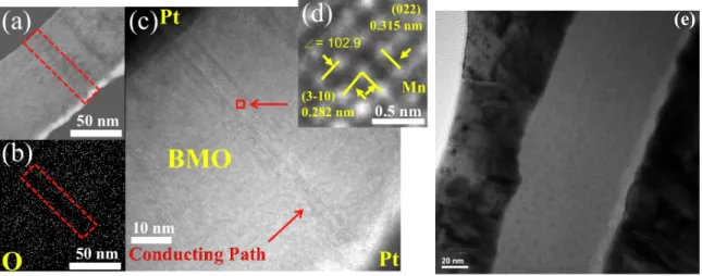
shows a low resistance state (LRS), considered as a nonvolatile on state in the RRAM device, which can be ascribed to the optimal redox conditions and thermal formation or ions migration of the conducting paths (CPs). The TEM high resolution result Fig. 16(a) shows current filament formed after resistive switching compared with Fig. 16(e), as the EDS mapping [Fig. 16(b)] displayed the oxygen vacancy and detail image shown as Fig. 16(c). the filament clearly presented in the (Bi, Mn)Ox profile
image. The structures had been recrystallized around the filament to form the conducting path through the (Bi, Mn)Ox thin film. The further evidence shown as Fig.
16(d) presented the metal manganese structure.
Fig. 16. TEM high resolution image after resistive switching displayed with (a) conducting path form in the (Bi, Mn)Ox thin film, (b) the EDS mapping of oxygen density, (c) local magnified image of
filament and inset of red square (d) shows the situation of arrangement of atoms and before resistive switching profile image shows in (e).
III.
The approach, step and progress of this topic
The major work is that how to repeat the high quality thin film. On the basis of this reason, it is necessary to grow new thin film for basically analyze and phase checking
like lattice structure measured by using instrument of X-Ray. The (Bi, Mn)Ox thin
films were deposited using pulsed laser deposition (COMPex-pro) with a KrF laser (λ=248 nm), a target-substrate distance of 6 cm and a repetition rate of 5 Hz and
grown on the c-oriented LaAlO3 (100) substrate (instrument image shown as Fig. 17).
The chamber was evacuated to a base pressure of 10-5 Torr and deposition was carried
out at 80 mTorr of oxygen background pressure. The deposition performed at 500 °C dependent on the deposition time. At last, temperature decrease with rate of 20 °C /min to room temperature under 300 Torr of oxygen background pressure (detail parameters of deposition shown as TABLE III).
Fig. 17. (a) PLD system include Excimer Laser and chamber. (b) chamber inside environment include
target, substrate.
Substrate Laser Beam Target
TABIE III. Deposition parameters of (Bi, Mn)Ox
The most important thing is that analysis of lattice structure, because of our (Bi,
Mn)Ox thin film display the new phase that reference papers have never seen before. So we design series of experiments to analyze the thin film structure and determine what phase such as using a high-resolution X-Ray diffractometer, film crystallinity was assessed, and film thickness was determined using low-angle reflectivity and
measured symmetry property in (Bi, Mn)Ox by four-circle high resolution x-ray
diffraction (XRD) (shown in Fig. 18) in National Synchrotron Radiation Research Center (NSRRC).
Until now working, we still keep analyzing the structure of (Bi, Mn)Ox thin film
and from the result, we supported that our thin film has two or more structures combined with manganite oxide and bismuth oxide. As result of Φ-scan, the in-plane scan displayed the different symmetric structures mixed in the same film. But these
data were not enough to determine the fine structure of (Bi, Mn)Ox thin film. We need
Fig. 18. The structural drawing of four-circle high resolution x-ray diffraction (Φ-scan ) site in the NSRRC.
The thin film surfaces were studied in tapping mode with a Multimode Atomic Force Microscope (AFM). The roughness of thin film surface decide the quality of
(Bi, Mn)Ox. If there are too many particles in the surface [shown in Fig. 19(a)] means the deposition parameters were not good. If the topic scan show the smooth surface [Fig. 19(b)] indicate that sample allowed to next step which scan by means of PFM shown as Fig. 19(d) to make sure the ferroelectric property. We can determine that the
nanostructure [Fig. 19(c)], domain structure or single phase in (Bi, Mn)Ox sample.
Fig. 19. Top view of AFM tapping mode scan with the result of (a) particles on sample surface, (b) smooth surface, (c) nanostructure and (d) phase diagram scanned by PFM.
(b) (a)
(c)
10. Dewar Isolation cabinet
11. Dewar
12. Printer
13. Magnetic power supply
14. Temp. controller
15. Console Cabinet
16. Power distribution unit
17.MPMS controller
18. Gas/Magnet control
unit
19. Computer
20. Monitor
In order to realize the magnetic behavior, we used the SQUID (Fig. 20) to study the magnetization behavior and cooperated with NSRRC to realize the valence of manganite and other magnetic properties. The temperature dependent on magnetic susceptibility (M-T curve) and apply magnetic field dependent on magnetic susceptibility (M-H curve) were measured using a Quantum Design® SQUID system
vibrating sample magnetometer with the magnetic field applied along an in-plane perpendicular to (100) LAO and out-plane parallel to (100) LAO direction. Prior to the magnetic measurements, the silver dag was removed from the back of the substrates with emery paper. As the result of the SQUID measurement, we can understand which kind of magnetic properties like ferromagnetic, antiferromagnetic,
diamagnetic and paramagnetic behaviors the (Bi, Mn)Ox belongs to.
We further search the valence of magnesium compared with different plane
between in-plane and out-of-plane using X-ray Magnetic Linear Dichroism (XMLD)
in NSRRC. Soft x ray magnetic dichroism spectroscopies play an ever increasing role
in improving our understanding of complex magnetic nanostructures as these techniques provide elemental and chemical site-specific magnetic information with high sensitivity and tunable probing depth. X ray spectromicroscopy techniques such as photoemission electron microscopy (PEEM) add spatial resolution down to a few nm. Using spectroscopic information for magnetometry and magnetic microscopy, i.e., to determine the alignment of magnetic moments relative to the crystal axes and to image domains, requires detailed knowledge and theoretical understanding of the spectral shape and magnitude of dichroism signals as well as their dependence on the relative orientation of polarization, external field, and crystallographic axes. Among these solution of XMLD measurement we performed to probe the valence of manganite (shown as Fig. 21) and determine the magnetic properties of (Bi, Mn)Ox.
Fig. 21. Mn L2,3-edges of TEY XAS spectra measured at 300 K in National Synchrotron Radiation Research Center in Taiwan.
Moreover, we in order to determine which kind of lattice structure of our sample, for example, lattice constant a, b, c axis, stoichiometry of element configuration, phase determination and geometric arrangement of crystallographic unit cell. After then, we will establish the mechanism to explain the magnetic behavior even
magnetoelectric coupling effect if it exist consist with TEM result. So that, The (Bi,
Mn)Ox thin film structure were measured by using Philips TECNAI-20 Transmission Electron Microscopy/Energy Dispersive Spectrometers (TEM/EDS).
The resistivity was obtained with four-point path measurement by closed cycle
refrigerator system (Tlowest = 13 K) from room temperature to 20 K (Fig. 22). Among
this measurement, we can check metal property of our sample.
Fig. 22. Resistance dependence of temperature (R-T) curve measured by four-point path cryogenic closed cycle refrigerator system.
Furthermore, we will use the LCR meter (Inductance (L), Capacitance (C), and
Resistance (R)) is a piece of electronic test equipment used to measure the inductance, capacitance and, resistance of a component. In the usual versions of this instrument these quantities are not measured directly, but determined from a measurement of impedance. The necessary calculations are, however, incorporated in the instrument's circuitry; the meter reads L, C and R directly with no human calculation required. We can further study electric properties by LCR meter which probe the polarization versus electric field (P-E) hystersis loops with E parallel and perpendicular to c-axis
of LAO substrate will be carried out at cryogenic temperatures. We can even apply the magnetic field into P-E measurement for deep study the magnetoelectric coupling effect.
Conclusion :
We searched the metal element bismuth combined with manganite thin film. In series of experiments such as XRD diffraction patterns to show the several phase of bismuth oxide and manganite mixed in the same thin film. At first, we identified the bismuth manganite target by used of XRD as possible structures of Bi2Mn4O10, Bi2MnO20 and Bi2O3, then the most stable repeatable condition of (Bi, Mn)Ox thin
film growth have been demonstrated by PLD system. AFM scanning process which measure the topographic pictures in which we decided the quality of (Bi, Mn)Ox thin
film and configuration of structure, SQUID resented the ferromagnetic properties, PFM displayed the ferroelectric behavior, and last XAS presented the mixed valence of Mn3+ and Mn4+ in our (Bi, Mn)Ox thin film. From these result led us to speculate that (Bi, Mn)Ox thin film has several possible structures such like Mn2O3, MnO2, Bi2O3, …etc, compared with data base. For application, we applied our sample to do the resistive switching in application of RRAM and obtained critical result.
Future work :
As result of our experiments, we have not sure about the fine structures of our thin film system. The following step of our experiment is to identify the fine structure of (Bi, Mn)Ox thin film dependence on magnetic behavior of powder measurement by using SQUID to compare with result of thin film. After then, we will measure the phi-scan of our sample to determine the lattice structure of (Bi, Mn)Ox thin film compare with result of magnetic properties and other several experiment, for example of TEM high resolution and diffraction pattern analysis.
Moreover, we will back to sinter our target of bismuth manganite to demonstrate the perovskite structure of BMO and then grow the thin film to compare with present sample. After all, the related magnetic properties such as spin structures will been probed as XAS cooperate with NSRRC and magnetoelectric coupling effect mechanism will be performed with (Bi, Mn)Ox and perovskite-type BMO thin film.
The application of RRAM will still keep performing and establish the mechanism for the high resistance state and low resistance state correspond with (Bi, Mn)Ox and perovskite-type BMO thin film cooperate with NTU.
Reference :
[1] Schmid,H.Multi-ferroicmagnetoelectrics.Ferroelectrics162, 665–685(1994).
[2] W. Eerenstein1, N. D. Mathur1 & J. F. Scott, Nature 442, 759-765 (17 August 2006).
[3] L.W. Martin, S.P. Crane, Y.-H. Chu, M.B. Holcomb, M. Gajek, M. Huijben, C.-H. Yang, N. Balke, R. Ramesh, J. Phys. Condens. Matter. 20 (2008) 434220.
[4] Hill, N. A. Why are there so few magnetic ferroelectrics? J. Phys. Chem. B 104, 6694–-6709(2000).
[5] Gajek, M. et al. Multiferroic tunnel junctions. Preprint at khttp://arxiv.org/condmat/0606444l (2006).
[6] Schmid, H. On a magnetoelectric classification of materials. Int. J. Magn. 4, 337–-361 (1973). [7] Ascher, E., Rieder, H., Schmid, H. & Sto ̈ssel, H. Some properties of ferromagnetoelectric nickel- iodine boracite, Ni3B7O13I. J. Appl. Phys. 37, 1404–-1405(1966).
[8] K.Terabe,T.Hasegawa,T.Nakayama,andM.Aono,“Quantizedconduc- tance atomic switch,” Nature, vol. 433, no. 7021, pp. 47–50, Jan. 2005.
[9] T. Sakamoto, H. Sunamura, H. Kawaura, T. Hasegawa, T. Nakayama, and M. Aono, “Nanometer- scale switches using copper sulfide,” Appl. Phys. Lett., vol. 82, no. 18, pp. 3032–3034, May 2003. [10] M. N. Kozicki, C. Gopalan, M. Balakrishnan, M. Park, and M. Mitkova, “Non-volatile memory based on solid electrolytes,” in Proc. NVMTS, 2004, pp. 10–17.
[11] S. Seo, M. J. Lee, D. H. Seo, E. J. Jeoung, D.-S. Suh, Y. S. Joung, I. K. Yoo, I. R. Hwang, S. H. Kim, I. S. Byun, J.-S. Kim, J. S. Choi, and B. H. Park, “Reproducible resistance switching in polycrystalline NiO films,” Appl. Phys. Lett., vol. 85, no. 23, pp. 5655–5657, Dec. 2004.
[12] A. Beck, J. G. Bednorz, C. Gerber, C. Rossel, and D. Widmer, “Repro- ducible switching effect in thin oxide films for memory applications,” Appl. Phys. Lett., vol. 77, no. 1, pp. 139–141, Jul. 2000. [13] Y. Watanabe, J. G. Bednorz, A. Bietsch, C. Gerber, D. Widmer, A. Beck, and S. J. Wind,
“Current-driven insulator–conductor transition and non- volatile memory in chromium-doped SrTiO3 single crystals,” Appl. Phys. Lett., vol. 78, no. 23, pp. 3738–3740, Jun. 2001.
[14] S. Tsui, A. Baikalov, J. Cmaidalka, Y. Y. Sun, Y. Q. Wang, Y. Y. Xue, C. W. Chu, L. Chen, and A. J. Jacobson, “Field-induced resistive switch- ing in metal-oxide interfaces,” Appl. Phys. Lett., vol. 85, no. 2, pp. 317– 319, Jul. 2004.
[15]G. A. Smolenskii and I. E. Chupis, Sov. Phys. Usp. 25, 475 (1982).
[16] T. Kimura, S. Kawamoto, I. Yamada, M. Azuma, M. Takano, and Y. Tokura, Phys. Rev. B 67, 180401(R) (2003).
[17] R.D. Shannon, Acta Crystallogr., Sect. A: Cryst. Phys., Diffr., Theor. Gen. Crystallogr. 32, 751 (1976).
(Leningrad) 7, 2993 (1966) (Sov. Phys. Solid State 7, 2993 (1966)).
[19] F. Sugawara, S. Iida, Y. Syono, and S. Akimoto, J. Phys. Soc. Jpn. 25, 1553 (1968).
[20] A. Moreira dos Santos, S. Parashar, A.R. Raju, Y.S. Zhao, A.K. Cheetham, and C.N.R. Rao, Solid State Commun. 122, 49 (2002).
[21] T. Atou, H. Chiba, K. Ohoyama, Y. Yamaguchi, and Y. Syono, J. Solid State Chem. 145, 639 (1999).
[22] I. Troyachuk, N.V. Samsonenko, E.F. Shapovalova, I.M. Kolesova, and H. Shymczak, J. Phys.: Condens. Matter 8, 11 205 (1996).
[23] F. Sugawara, S. Iida, Y. Syono, and S.-i. Akimoto, J. Phys. Soc. Jpn. 20, 1529 (1965).
[24] V. Bokov, I.E. Myl’nikova, S.A. Kizaev, M.F. Bryzhina, and N.A. Grigoryan, Fiz. Tverd. Tela (Leningrad) 7, 2993 (1966) (Sov. Phys. Solid State 7, 2993 (1966)).
[25] A. Moreira dos Santos and A. K. Cheetham, T. Atou, Y. Syono, Y. Yamaguchi, K. Ohoyama, and H. Chiba, PHYSICAL REVIEW B 66, 064425 (2002).
[26] J.B. Goodenough, Phys. Rev. 100, 564 (1955).
[27] J.B. Goodenough, J. Phys. Chem. Solids 6, 287 (1958). [28] J. Kanamori, J. Phys. Chem. Solids 10, 87 (1959).
[29] W. Eerenstein, F. D. Morrison and J. F. Scott, N. D. Mathur, Appl. Phys. Lett. 87, 101906 (2005). [30] E. Ohshima, Y. Saya, M. Nantoh, and M. Kawai, Solid State Commun. 116, 73 (2000).
[31] H. Faqir, H. Chiba, M. Kikuchi, Y. Syono, M. Mansori, P. Satre, and A. Sebaoun, J. Solid State Chem. 142, 113 (1999).
[32] Ramesh, R.; Spaldin, N. A. Nat. Mater. 2007, 6, 21.
[33] Eerenstein, W.; Mathur, N. D.; Scott, J. F. Nature 2006, 442, 759. [34] Khomskii, D. I. J. Magn. Magn. Mater. 2006, 306, 1.
[35] Fiebig, M. J. Phys. D: Appl. Phys. 2005, 38, R123.
[36] Baettig, P.; Ederer, C.; Spaldin, N. A. Phys. ReV. B 2005, 72, 214105.
[37] Sugawara, F.; Iiida, S.; Syono, Y.; Akimoto, S. J. Phys. Soc. Jpn. (1968), 25, 1553.
[38] Tomashpol’skii, Y. Y.; Zubova, E. V.; Burdina, K. P.; Venevtsev, Y. N. Inorg. Mater. (1967), 3, 1861.
[39] Atou, T.; Chiba, H.; Ohoyama, K.; Yamaguchi, Y.; Syono, Y. J. Solid State Chem. (1999), 145, 639.
[40] Seshadri, R.; Hill, N. A. Chem. Mater. (2001), 13, 2892.
[41] Moreira dos Santos, A.; Cheetham, A. K.; Atou, T.; Syono, Y.; Yamaguchi, Y.; Ohoyama, K.; Chiba, H.; Rao, C. N. R. Phys. ReV. B (2002), 66, 064425.
[42] Kimura, T.; Kawamoto, S.; Yamada, I.; Azuma, M.; Takano, M.; Tokura, Y. Phys. ReV. B (2003), 67, 180401(R).
[43] Zavaliche, F., et al., Appl. Phys. Lett. (2005) 87, 182912. [44] Zavaliche, F., et al., Appl. Phys. Lett. (2005) 87, 252902. [45]Zavaliche, F., et al., Phase Transit. (2006) 79, 991.
[46] H. Wadati,D. G. Hawthorn, T. Z. Regier, G. Chen, T. Hitosugi, T. Mizokawa, A. Tanaka, and G. A. Sawatzky, Appl. Phys. Lett. 97, (022106).
[47] A. N. Vasiliev, O. S. Volkova, L. S. Lobanovskii, I. O. Troyanchuk, Z. Hu, L. H. Tjeng, D. I. Khomskii, H.-J. Lin, C. T. Chen, N. Tristan, F. Kretzschmar, R. Klingeler, and B. Buchner, Phys. Rev. B 77, 104442 (2008).
[48] D. R. Lamb and P. C. Rundle, Br. J. Appl. Phys. 18, 29-32 (1967).
[49] I.-S. Park et al., Jap. J. Appl. Phys. vol. 46, pp. 2172-2174 (2007). [50] D. Lee et al., Appl. Phys. Lett. 90, 122104 (2007).
[51] I. G. Baek, M. S. Lee, S. Seo, M. J. Lee, D. H. Seo, D. S. Suh, J. C. Park, H. S. Kim, I. K. Yoo, U. I. Chung, and J. T. Moon, in IEDM Tech. Dig., 2004, pp. 587–590.
[52] Wen-Yuan Chang, Yen-Chao Lai, Tai-Bor Wu,Sea-Fue Wang, Frederick Chen, and Ming-Jinn Tsa, Appl. Phys. Lett. 92, 022110 (2008).
[53] Chih-Yang Lin, Dai-Ying Lee, Sheng-Yi Wang, Chun-Chieh Lin, Tseung-Yuen Tseng, Surface & Coatings Technology 203 (2008) 628–631.
[54] Gyeong-Su Park, Xiang-Shu Li, Dong-Chirl Kim, Ran-Ju Jung, Myoung-Jae Lee, and Sunae Seo, Appl. Phys. Lett. 91, 222103 (2007).
國科會補助專題研究計畫項下出席國際學術會議心得
報告
日期: 2012 年 5 月 31 日一、參加會議經過
By this trip in Boston, that’s a beautiful city but very cold. By this time with conference called APS, I learned lots of new idea with my topic. For example, XSTM can realized the band gap and band structure between two different structures at interface like band banding. When my oral come, I introduced my topic and one professor asked me some suggested questions help me to advanced realize another way if my topic after oral. The fourth day, I joined the session : “Interfaces in Complex Oxides-Electronic, Magnetic and Optical Properties” and listened to the topic : “First principles insights into electronic, magnetic, and dynamic effects at and across oxide interfaces”.
二、與會心得
In this APS conference I presented at several sessions not totally the same domain because I wanted to learn something different beside my focused research. There are new knowledge in other domain study and help me to establish frame of experiment and broaden my horizons for example, the complex oxides thin film
計畫編號 NSC 98-2112-M-009-007-MY3 計畫名稱 強關聯量子物質之材料、界面、與其衍生性物理特性研究- 子計畫四:強關聯量子材料及結構之相分離研究 出國人員 姓名
郭韋呈
服 務 機 構 及 職 稱 國 立 交 通 大 學 電子物理系 會議時間 101 年 2 月 26 日 至 101 年 3 月 2 日 會 議 地 點 美國-波士頓 會議名稱(中文)美國物理年會
(英文) American Physical Society
發表論文 題目
(中文)以掃描穿遂顯微鏡探討異質結構鍶錳氧/鑭
錳氧之特性
(英文)
Cross-sectional Scanning Tunneling Microscopy
(XSTM) Investigation on
(SrMnO
3)
n/( LaMnO
3)
nand nanostructures have different domain accompany different direction of polarization cased ferroelectric properties. Their result helps me to realize deeply on my topic.
三、考察參觀活動
(無是項活動者略)
四、建議
I suggest that our government can imitate the way dependence of American physical society holding in the building like a convention center because the presentation room all together in the same building and we can go convenience to any session place. Further more, there are restaurants in the convention center for visitors, we can eat directly if do not want to go outside. We should invite a little more famous speaker separate from any domain of sciences to give advanced knowledge.
五、攜回資料名稱及內容
The topic which title is Electrically controllable spontaneous magnetism in nanoscale mixed phase multiferroics is a great helpful for me. The abstract is that magnetoelectrics and multiferroics present exciting opportunities for electric-field control of magnetism. However, there are few room-temperature ferromagnetic-ferroelectrics. Among the various types of multiferroics the bismuth ferrite system has received much attention primarily because both the ferroelectric and the antiferromagnetic orders are quite robust at room temperature. Here we demonstrate the emergence of an enhanced spontaneous magnetization in a strain-driven rhombohedral and super-tetragonal mixed phase of BiFeo3. using X-ray magnetic circular dichroism-based photoemission electron microscopy coupled with macroscopic magnetic measurements, we find that the spontaneous magnetization of the rhombohedral phase is significantly enhanced above the canted antiferromagnetic moment in the bulk phase, as a consequence of a piezomagnetic coupling to the adjacent tetragonal-like phase and the epitaxial constraint. Reversible electric-field control and manipulation of this magnetic moment at room temperature is also shown.
六、其他
I obtained much useful novel knowledge from other domain of sciences and had a wonderful experience of life in America.
國科會補助專題研究計畫項下出席國際學術會議心得
報告
日期: 2012 年 5 月 31 日一、參加會議經過
學生朱培源於101 年 2 月 26 至 3 月 2 日參加美國物理年會於波士頓,會議 期間參與許多方面的物理演說,包括凝態計算物理、固態物理實驗、新的 超導體材料、發光元件、磁性材料、以及最熱門的拓撲絕緣體。二、與會心得
在參加完了會議之後,並激起了許多實驗上的靈感,雖然實驗上的方法不盡 相同,但是在加了我們學校上儀器與師資上的優勢(核磁共振系統、超導量子 干涉儀、AFM 與 TEM),可以讓我們更加瞭解新穎的物理行為。三、考察參觀活動(無是項活動者略)
四、建議
計畫編號 NSC 98-2112-M-009-007-MY3 計畫名稱 強關聯量子物質之材料、界面、與其衍生性物理特性研究- 子計畫四:強關聯量子材料及結構之相分離研究 出國人員 姓名朱培源
服 務 機 構 及 職 稱 國 立 交 通 大 學 電子物理系 會議時間 101 年 2 月 26 日 至 101 年 3 月 2 日 會 議 地 點 美國-波士頓 會議名稱(中文)美國物理年會
(英文) American Physical Society
發表論文 題目
(中文)在矽基板上成長氧化鋅產生室溫發光效應
(英文)
Enhanced Free Excition and Direct Band-Edage
Emissions at Room Temperature in ZnO Films Grown on
Si Nanopillars by Atomic Layer Deposition
近來已著手相關的實驗流程,也有顯著的發現,全因在不同的地方增廣視野, 也希望在未來能讓更多的同學與老師們,參與國際型會議增加學術交流的機 會。
五、攜回資料名稱及內容
六、其他
國科會補助專題研究計畫項下出席國際學術會議心得
報告
日期: 2012 年 5 月 31 日一、參加會議經過
會議第一天,在已經相當龐大的會場中湧入了滿滿的人潮,仔細搜尋一番,不 難發現發現許多物理大師與諾貝爾得主的身影,如伊利諾大學,Prof. Lane Martin, 英國劍橋大學,Prof. James Scott, 與新科諾貝爾獎得主等等…會議第一 天早上八點學生完成註冊後,便於各大Session中聽取來自世界各地之傑出教授, 博士後,博士生之論文發表與討論,第一天包涵邀請演講與論文發表在內,約 有一千兩百人次之講座,為此過程中學生僅挑出同領域中代表性之演說與發表 參加,有問題的地方學生會加以提出並尋求專家之意見,第一天會議結束於約 下午五點半,令人獲益良多。 計畫編號 NSC 98-2112-M-009-007-MY3 計畫名稱 強關聯量子物質之材料、界面、與其衍生性物理特性研究- 子計畫四:強關聯量子材料及結構之相分離研究 出國人員 姓名武卿亞
服 務 機 構 及 職 稱 國 立 交 通 大 學 物理研究所 會議時間 101 年 2 月 26 日 至 101 年 3 月 2 日 會 議 地 點 美國-波士頓 會議名稱(中文)美國物理年會
(英文) American Physical Society
發表論文 題目
(中文) 二維電子氣在異質介面之鐵電特性之控制
(英文)
Ferroelectric control of two dimensional
會議第二天,學生挑戰最新學術與工業界研究都相當熱門之topological insulator議題參加,過程中學生聽取了三個邀請演講與約十個發表演講,獲益 極多,也因此學生在會議中得到一些結合graphene與學生現今研究之議題之想 法,並與同樣參與本次會議的指導老師討論,獲得指導老師相當正面之評價。 學生並於第二天晚上參加由國家同步輻射中心,台灣大學,清華大學與成功 大學共同舉辦之台灣之夜晚宴,晚宴中,由許多學術界中大名鼎鼎之前輩發 表演說與鼓勵,中研院,國科會也藉此發表正在興建中之國家光子源之願景 與建構過程。交通大學物理所所長林老師也於其中分享本校之成功經驗與願 景,相當精采。 會議第三天,學生於上午發表論文演說,演說過程順利,並成功獲得台下專 家的共鳴。 會議第四天,有了第三天的成功經驗,學生對自我更加抱有信心與期待, 於第四天的會議期間,再次挑出兩個邀請演說與十一個發表演說參加學習, 於第四天也遇到來自成大物理與中山物理的陳宜君老師與邱雅萍老師,兩位 老師邀請學生與其研究生一同參加晚餐,並於晚餐過程中與台灣的學術前輩 熱烈討論,也藉此經驗認識不少同年齡層之研究夥伴。 會議第五天,亦是會議的最後一天,學生再次選擇一個邀請演講與五個 發表論文演講參加,整個會議於下午結束,為大會畫下完美句點,與指導 老師與會議中認識的老師與同學們先約下次再見。
二、與會心得
此次會議為學生第一次到美國參與世界級頂級會議,會議中,除了聽取世界 各大物理領域的專家演說以外,也聽取世界各地的教授們,博士後與博士的 發表演說,除了學習到各種不同的演說技巧與方法,更跨領域地學到不同領 域的專業知識,為學生的研究生涯注入活血。三、考察參觀活動(無是項活動者略)
四、建議
相當感謝學校與教育部的補助與資助,唯跨州至歐美之機票,註冊費用與生 活費用皆偏高,為此即使學生得到相對高額之補助,但對於家境較困難之學 生則仍然吃力許多,希望學校與相關單位,能適量的提高,或修改相關的補 助規範,讓表現優良但經濟環境吃緊的學生可以有更多躍上國際舞台的機會。五、攜回資料名稱及內容
Title: Ferroelectric control of two dimensional electron gas in oxide
heterointerface Content of conference data (please see my attached file of ppt.)
六、其他
本次學生第一次於國外參與國際會議,首先謝謝國科會與學校單位提供本次之 部分補助讓學生得以成形,研究工作為國家基本建設與研究之基石,希望有機 會或預算寬裕時可以多補助學生們類似的預算,台灣國際能見度也能藉由這些 機會與會議交流中,進而大量提昇台灣國際能見度。國科會補助專題研究計畫項下出席國際學術會議心得
報告
日期: 2012 年 6 月 31 日一、參加會議經過
On the first day, the meeting start at eight o’clock. This is also the first day for the participate complete their registration. I attended some major sessions to listen to the distinguished professor around the world, post-doctoral, thesis published with discussions. On that day, I listened the speech of Prof. Ron Rouff with title: “Graphene – based and graphene derived materials and their properties. In this object, I realized that graphene based materials are promising because of their electronic and thermal transport, mechanical properties, high specific surface area, that they can act as an atom thick layer, barrier or membrane. In addition, I also attended the talk “ MEMS: the Ideal Intergrated Functionality” of Prof. Kurt Petersen which I can learn a alot from this talk. The presentation about no silicon-based technology fits the definition of “more than Moore” better than MEMS. Beginning as an obscure cottage industry about 40 years ago, MEMS has grown to a $10B market which touches the
計畫編號 NSC 98-2112-M-009-007-MY3 計畫名稱 強關聯量子物質之材料、界面、與其衍生性物理特性研究- 子計畫四:強關聯量子材料及結構之相分離研究 出國人員 姓名
武卿亞
服 務 機 構 及 職 稱 國 立 交 通 大 學 物理研究所 會議時間 101 年 6 月 19 日 至 101 年 6 月 20 日 會 議 地 點 香港-香港理工大學 會議名稱(中文)
(英文) International Symposium on Integrated
Functionalities
發表論文題目

![FIG. 13. (a) Mn 2p XAS spectra and their comparison with the reference data of Mn 2+ (MnO), Mn 3+ (LaMnO 3 ), and Mn 4+ (EuCo 0.5 Mn 0.5 O 3 and SrMnO 3 ) from Ref [47], (b) Mn L 2,3 -edges of TEY](https://thumb-ap.123doks.com/thumbv2/9libinfo/8439888.181784/22.892.128.780.756.1064/fig-spectra-comparison-reference-lamno-euco-srmno-edges.webp)