國 立 交 通 大 學
電子工程學系 電子研究所碩士班
碩 士 論 文
利用原子層沉積系統成長氧化鋁閘極介
電層於砷化鎵基板之研究
Al
2O
3Gate Dielectric on GaAs by Atomic
Layer Deposition System
研 究 生:張 競 之
指導教授:簡 昭 欣 博士
利用原子層沉積系統成長氧化鋁閘極介
電層於砷化鎵基板之研究
Al
2O
3Gate Dielectric on GaAs by Atomic
Layer Deposition System
研 究 生:張 競 之 Student:Ching-Chih Chang
指導教授:簡 昭 欣 博士 Advisor:Chao-Hsin Chien
國 立 交 通 大 學
電子工程學系電子研究所碩士班
碩 士 論 文
A ThesisSubmitted to Department of Electronics Engineering & Institute of Electronics College of Electrical and Computer Engineering
National Chiao Tung University in partial Fulfillment of the Requirements
for the Degree of Master
in
Electronics Engineering & Institute of Electronics June 2007
Hsinchu, Taiwan, Republic of China
利用原子層沉積系統成長氧化鋁閘
極介電層於砷化鎵基板之研究
研 究 生:張 競 之 指 導 教 授:簡 昭 欣 博士
國立交通大學
電子工程學系電子研究所碩士班
摘 要
砷化鎵擁有高電子遷移率、較大的能帶隙、功率耗損低及較大的崩潰電場 等優點,因此用它取代矽基板做電晶體等應用具有可行性。 就砷化鎵晶圓的濕式化學清洗而言,我們希望能夠達到抑制原生氧化層的 效果。從 XPS 分析圖發現,當鹽酸濃度的比例下降,對於抑制原生氧化層的能 力愈佳。然而,低於鹽酸濃度 10%,對於砷的氧化物的去除能力,是呈現負成 長。除此之外,如果在鹽酸中加入雙氧水,基板更容易被氧化,產生更厚的原 生氧化層,因此降低了清洗的能力。同時,我們也發現硫化銨溶液對於原生氧 化層的抑制也具有效用。 我們利用原子層沉積系統成長氧化鋁作為閘極介電層。就漏電因素而言, 我們選擇基板加熱至 300o C,然後再沉積氧化鋁,除此之外,亦使用交界鈍化層(IPLs)試圖使沉積在基板上的薄膜能夠有較佳的效果,其中,疊上一層薄薄的 矽及硫化銨鈍化是兩種最常見的交界鈍化層。並且發現,這兩種方法確實對於 抑制原生氧化層有很大的功效,而且有助於沉積高品質的氧化鋁薄膜,尤其是 將清洗完的砷化鎵基板浸泡在硫化銨溶液中。我們亦研究出,使用硫化銨溶液 約 2%並浸泡至其中 30 秒為硫鈍化的最佳效果。 在長完氧化鋁之後,將晶圓做沉積後快速熱退火(PDA)並試圖讓薄膜較佳 化。在做完 600o C 快速熱退火之後,C-V 曲線的確變得更陡峭,而遲滯現象也降 低了,但是卻造成漏電流變大,尤其是在氮氣環境下做快速熱退火。這是因為 在氮氣環境下比起在氧氣環境下產生了較多的砷與砷的鍵結(As layer)於介電 層裡,而這種鍵結是在氧化鋁薄膜中形成漏電流的最主要的因素。 最後討論電容結構的可靠度問題。發現,隨著應力的增加,做硫化銨鈍化 的樣品,更能承受應力使得漏電流不至於增加太快。當我們考慮漏電流、遲滯 現象以及接面載子補捉密度(Dit),則認為有做硫鈍化以及在氧氣環境下做快速 熱退火,是最佳的選擇。
Al
2O
3Gate Dielectric on GaAs by Atomic
Layer Deposition System
Student:Ching-Chih Chang Advisor:Dr. Chao-Hsin Chien
Department of Electronics Engineering and Institute of Electronics
National Chiao Tung University, Hsinchu, Taiwan
Abstract
GaAs offers the advantages of high electron mobility, rich band gap engineering, low power consumption and high breakdown fields and thus is expected to outperform Si in the specific metal-oxide-semiconductor (MOS) applications.
With wet-chemical cleaning of GaAs wafers, it is necessary to effectively suppress the formation of native oxide before dielectric deposition. From XPS spectra, we found that HCl solution could better eliminate native oxide with decreasing concentration, but with a limit of around 10%. Less than 10%, the situation became worse. Moreover, as we used the mixture solution of HCl and H2O2, the substrates would be oxidized and cleaning
effect decreased. We also found that (NH4)2S passivation was effective in suppression of
In this thesis, we grew Al2O3 by atomic layer deposition system (ALD). For low
leakage current, the growth temperature was set at 300o
C. Prior to dielectric deposition, we employed additional interfacial passivation layers (IPLs) in order to deposit excellent Al2O3 film. Si capping and (NH4)2S passivation were the two most commonly used IPLs
techniques. We found that these two methods were effective in eliminating native oxide and in turn very helpful in achieving high-quality Al2O3 film deposition. In particular, we
found that dipping in 2% (NH4)2S solution for 30s was the optimized treatment condition.
After depositing Al2O3, we conducted post deposition annealing (PDA) to further
improve the deposited film. We observed that the C-V curves of the samples became sharper and their hysteresis decreased significantly with PDA at 600o
C concomitant with larger leakage current, especially in N2 atmosphere. We believe it is due to the fact that
N2 annealing would cause more As layer incorporated into the dielectric than O2, which is
likely to form the leakage current path.
Finally, the reliability of MOS capacitors has been characterized and discussed. It was observed that (NH4)2S treatment was effective in preventing rapid Jg increase during
stressing. Considering not only Jg, hysteresis but also Dit, O2 PDA with sulfide treatment
誌 謝
兩年,說長不長,說短不短,但是我在這兩年期間,完成了碩士學位。儘 管過得跌跌撞撞,所有的東西,從無到有,靠著大家的幫忙,在拼拼湊湊之下, 終於完成了我的第一本論文。 首先要感謝我的指導老師 簡昭欣 博士,您是最大的功臣,總是讓我資源 充足,無後顧之憂的前進。感謝兆欽學長,當學弟有實驗或分析上的問題時, 一定會放下手邊的事情,為我解決困難;也要謝謝明瑞學長,辛苦的帶我們討 論 paper,讓我們了解更多。 同時,也要感謝國家儀科中心的蕭健男副組長,願意提供機台讓我做研究; 更要感謝同樣身為屏東人的志忠學長,除了在儀器使用上給予支援,在一個陌 生的地方能夠遇到同鄉人,總是親切,並給我更多的鼓勵;還要謝謝清大材料 博士班致傑學長的儀器教學及歡樂。 謝謝我的實驗伙伴曾治國,總是不厭其煩的提醒我,並給我實驗支援,讓 我不致於顧此失彼;也要感謝其他要一起畢業的實驗室同學以及學弟,還有我 的大學同學,有你們的陪伴,為煩悶的生活裡注入了更多快樂的元素。 除此之外,更要感謝我的父母,將我栽培長大,雖然曾經讓你們失望,但 是沒有你們一路的支持,也沒有今天的我;我的阿公,電話裡有你的聲音,讓 我心裡感覺更安心;還有姐姐,不斷的給我生活上的協助,從家裡幫我帶來媽 媽的愛心,讓我的煩燥生活充滿更多愉快。 感謝佩琪,從大學到碩士畢業,經歷了一千多個日子,給我更多的支持與 鼓勵,讓我身邊多了一隻手,時時拉著我。 最後,祝福每一個曾經幫助以及陪伴著我的人,過著愉快的生活。
Contents
Abstract (Chinese)
... IAbstract (English)
...IIIAcknowledgement
... VContents
...VIFigure Captions
...IXTable Captions
... XVChapter 1 Introduction
---11-1
General Background
---11-2
Motivation
---31-3
Organization of the Thesis
---5Chapter 2 The Cleaning Process of GaAs Substrate
---92-1
Introduction
---92-2
Experimental Procedures
--- 102-3
Results and Discussion
--- 11Chapter 3 Atomic Layer Deposited Al
2O
3on GaAs
--- 243-1
Introduction
--- 243-2
Experimental Procedures
--- 253-3
Results and Discussion
--- 263-3-1 ALD Temperature optimization--- 26
3-3-2 Interfacial Passivation Layer on GaAs --- 27
3-4
Summary
--- 31Chapter 4 Thermal Effect of Al
2O
3/GaAs by ALD
--- 454-1
Introduction
--- 454-2
Experimental Procedures
--- 464-3
Results and Discussion
--- 474-3-1 Electric and Physical Characteristics --- 47
4-3-2 Reliability Issues --- 50
4-4
Summary
--- 51Chapter 5 Conclusions and Future Work
--- 645-1
Conclusions
--- 64References
...70Figure Captions
Chapter 1 Introduction
Fig. 1-1 The equivalent oxide thickness versus generation technology node for (a) microprocessor and (b) low power.
Fig. 1-2 J limit versus Jg simulated for high-performance logic.
Fig. 1-3 Energy gap versus dielectric constant for SiO2, Si3N4, Al2O3, ZrSiO4, HfSiO4,
ZrO2, and HfO2.
Chapter 2 The Cleaning Process of GaAs Substrate
Fig. 2-1 XPS spectrum As 2p3 after different cleaning processes of table 2 Fig. 2-2 XPS spectrum As 3d after different cleaning processes of table 2 Fig. 2-3 XPS spectrum Ga 2p3 after different cleaning processes of table 2 Fig. 2-4 XPS spectrum Ga 3d after different cleaning processes of table 2 Fig. 2-5 XPS spectrum As 2p3 after different cleaning processes of table 4 Fig. 2-6 XPS spectrum As 3d after different cleaning processes of table 4 Fig. 2-7 XPS spectrum Ga 2p3 after different cleaning processes of table 4 Fig. 2-8 XPS spectrum Ga 3d after different cleaning processes of table 4
solution
Fig. 2-10 XPS spectrum As 3d of cleaning substrates with or without (NH4)2S solution
Fig. 2-11 XPS spectrum Ga 2p3 of cleaning substrates with or without (NH4)2S
solution
Fig. 2-12 XPS spectrum Ga 3d of cleaning substrates with or without (NH4)2S solution
Chapter 3 Atomic Layer Deposited Al
2O
3on GaAs
Fig. 3-1 Atomic layer deposition (ALD) reaction mechanism Fig. 3-2 ALD apply on IC fabrication (Juppo, 2001) [47]
Fig. 3-3 Multi-frequency C-V characteristics of MOS capacitors (Pt/Al2O3/GaAs) by
ALD (60 cycles) at (a) 100o
C (b) 300o
C
Fig. 3-4 Growth rate of different surface temperature (K) on Si
Fig. 3-5 The effect of temperature on J-V characteristics of Pt/Al2O3/GaAs MOS
capacitor made by ALD (60cycles)
Fig. 3-6 Dit vs. Vg characteristics of Pt/Al2O3/GaAs MOS capacitor made by ALD
(60cycles) at 100o
C and 300o
C
Fig. 3-7 Jg vs. CET for MOS capacitors (Pt/Al2O3/GaAs) made by ALD (100oC and
300o
Fig. 3-8 C-V (10 kHz) curves of Pt/Al2O3/GaAs MOS capacitors with different IPLs.
The Al2O3 was deposited by ALD (300oC, 60 cycles).
Fig. 3-9 XPS spectra (a) As 2p3 and (b) Ga 2p3 after ALD-Al2O3 (300oC, 60cycles)
Fig. 3-10 XPS spectra (a) As 3d and (b) Ga 3d after ALD-Al2O3 (300oC, 60cycles)
Fig. 3-11 Multi-frequency C-V characteristics of MOS capacitors (Pt/Al2O3/GaAs)
without and with sulfide passivation. The Al2O3 was deposited by ALD
(300o
C, 60 cycles).
Fig. 3-12 C-V curves of Pt/ Al2O3/GaAs capacitors before and after 400oC PMA. The
Al2O3 was deposited by ALD (300oC, 60 cycles).
Fig. 3-13 Jg versus different IPLs for Pt/Al2O3/GaAs MOS capacitors made by ALD
(300o
C, 60 cycles)
Fig. 3-14 (a) C-V characteristics of Pt/Al2O3/GaAs MOS capacitors without IPL and
(b) ΔC and ΔV versus different IPLs by ALD (300o
C, 60 cycles)
Fig. 3-15 C-V (10 kHz) curves of Pt/Al2O3/GaAs MOS capacitors with different IPLs.
The Al2O3 was deposited by ALD (300oC, 60 cycles).
Fig. 3-16 Plot of the ac loss (Gp/ω) vs. frequency for different biases on
Pt/Al2O3/GaAs MOS capacitors by ALD (300oC, 60) cycles without IPL
Fig. 3-17 Interface state density (Dit) as a function of gate voltage for MOS capacitors
(Pt/AlO/GaAs) made by ALD (300o
Fig. 3-18 Dit versus different IPLs for MOS capacitors Pt/Al2O3/GaAs made by ALD
(300o
C, 60 cycles)
Fig. 3-19 Gate leakage current density versus different IPLs for Pt/Al2O3/GaAs MOS
capacitors made by ALD (300o
C, 60 cycles)
Chapter 4 Thermal Effect of Al
2O
3/GaAs by ALD
Fig. 4-1 C-V curves at 10 kHz of MOS capacitors (Pt/Al2O3/GaAs) with and without
O2 600oC PDA 60s
Fig. 4-2 Typical 10 kHz C-V curves of Pt/Al2O3/GaAs capacitors with and without
O2 600oC PDA 60s
Fig. 4-3 Leakage current density Jg vs. Vg in the accumulation regime for
Pt/Al2O3/GaAs capacitors with and without O2 600oC PDA 60s
Fig. 4-4 Multi-frequency C-V characteristics of MOS capacitors (Pt/Al2O3/GaAs)
with O2 and N2 600oC PDA. The Al2O3 was deposited by ALD (300oC, 100
cycles)
Fig. 4-5 Multi-frequency C-V characteristics of MOS capacitors (Pt/Al2O3/GaAs)
with O2 and N2 600oC PDA. The Al2O3 was deposited by ALD (300oC, 60
Fig. 4-6 Typical 10 kHz C-V curves of Pt/Al2O3/GaAs capacitors with N2 and O2
600o
C PDA 60s. The sulfide treatment was the same as figure 4-5.
Fig. 4-7 Leakage current density Jg vs. Vg in the accumulation regime for
Pt/Al2O3/GaAs capacitors with N2 and O2 600oC PDA 60s
Fig. 4-8 The HRTEM images of N2 PDA Al2O3 film by ALD 100 cycles on GaAs.
The sulfide treatment was the same as figure 4-5.
Fig. 4-9 The HRTEM images of O2 PDA Al2O3 film by ALD 100 cycles on GaAs.
The sulfide treatment was the same as figure 4-5.
Fig. 4-10 The HRTEM images of O2 PDA Al2O3 film by ALD 60 cycles on GaAs.
The sulfide treatment was the same as figure 4-5.
Fig. 4-11 Dependence of CET on physical thickness of Al2O3 on Pt/Al2O3/GaAs MOS
capacitors with O2 and N2 600oC PDA
Fig. 4-12 Jg versus CET for Pt/Al2O3/GaAs MOS capacitors with O2 and N2 600oC
PDA
Fig. 4-13 XPS spectra As 2p3 and Ga 2p3 after 600o
C PDA. Passivation was (NH4)2S:H2O=1:20, dipping 5 min.
Fig. 4-14 The leakage current density (Jg) as a function of stress time after constant
Fig. 4-15 Hysteresis as a function of stress time after constant voltage stress (a) Vg =
4.5 V (b) Vg = 4.8 V
Fig. 4-16 The interface state density (Dit) after constant voltage stress Vg = 4.5 V as a
function of stress time
Chapter 5 Conclusions and Future Work
Fig. 5-1 Jg vs. CET for MOS capacitors (Pt/Al2O3/GaAs) made by ALD-300oC and
sputtering
Fig. 5-2 Multi-frequency C-V characteristics of MOS capacitors (Pt/Al2O3/GaAs)
with and without AlON
Fig. 5-3 Typical 10 kHz C-V curves of Pt/Al2O3/GaAs capacitors with and without
AlON
Fig. 5-4 Leakage current density Jg vs. Vg in the accumulation regime for
Table Captions
Table 1 Properties of undoped semi-conductors at 300K
Table 2 Wet-chemical cleaning processes (WCP) used in this study
Table 3 Chemical ratio by XPS spectra of As 2p3 and Ga 2p3 according to different cleaning processes
Table 4 Wet-chemical cleaning processes (WCP) used in this study
Table 5 Chemical ratio by XPS spectra of As 2p3 and Ga 2p3 according to different cleaning processes
Table 6 Average of Dit and Jg at CET = 40 Å of Pt/Al2O3/GaAs MOS capacitor made
by ALD at 100o
C and 300o
C
Chapter 1
Introduction
1-1 General Background
As the dimensions of complementary metal oxide semiconductor (CMOS) devices are scaled down to keep the continuous improvement on device performance, the thickness of the traditional SiO2 gate dielectric will steadily decrease to 1.2 nm, which resulting in large
leakage current and poor reliability. According to the first order current-voltage relationship, the ideal drive current IDS in a n-channel MOSFET can be expressed as
2 1 ( ) ( ) 2 ox DS n GS T ox W I V V t L ε μ = − (1.1) where εox is the permittivity of gate oxide, t is the gate oxide thickness, ox μn is the mobility for electrons, W is the channel width, L is the effective channel length, VGS is the applied gate-to-source voltage and V is the threshold voltage. In addition to T decrease the gate oxide thickness, others of the parameters in the above equation can be adjusted to improve the device driving capability. However, large VGS apparently creates an undesirably high electric field across the gate oxide, and the device reliability will be deteriorated in turn. Moreover, the reduction of V about 200 mV is limited because of T the induced statistical fluctuations in thermal energy at a typical operation circumstance of up to 100o
gate oxide capacitance are simple to achieve the higher driving current and chip density, directly. Although the scaling down of Si device dimensions is a continuous solution in the past two decades, the feature sizes of conventional Si MOSFETs have approximate to its fundamental physical limits. Therefore, new materials with higher electron mobility and novel device structures must be developed.
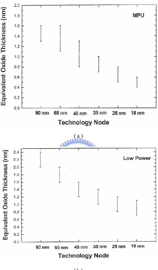
Currently, the CMOS technology node of 90 nm is well developed. According to the International Technology Roadmap for Semiconductors (ITRS) [1], the equivalent oxide thickness (EOT) should be less than 1.6 nm for next generation. Figure 1-1 (a) and (b) depict the shrinking trend of EOT as a function of technology node for microprocessor and low power devices. Although silicon oxy-nitride (SiON) gate dielectric has replaced SiO2
to achieve 90 nm technology node by its better dielectric integrity and lower stress induced leakage current, the dielectric constant of SiON is not high enough for 65 nm technology node. Besides, as the thickness is less than 1.2 nm, the direct tunneling effect will be a very critical issue to overcome. Thus, the resulting gate leakage current will not only degrade the performances of devices but increase the power dissipation. From figure 1-2, the leakage current limit cannot be met by using SiON after 2008. Therefore, the high dielectric constant (high-k) materials are imperious demands.
Recently, high-k materials such as Al2O3, ZrO2, HfO2, and their silicates [2-14] have
inversely proportional to their band-gap, as shown in figure 1-3 [15]. The narrower band-gap and smaller band offset would enhance Schottky emission of carriers. Furthermore, the trap-assisted tunneling, Frenkel-Poole emission and the hopping effect should be still solved. Consequently, there are several issues must be improved before those high-k materials replace SiO2 and SiON.
(1) Thin interfacial layer
(2) Low interface state density (Dit<1011 eV/cm2)
(3) Low gate leakage current (4) Good gate compatibility (5) Good thermal stability (6) Less mobility degradation
Moreover, a higher carrier transport in MOSFETs is considered through the increase of channel mobility. On the other hand, we could replace Si substrates by III-V compound substrates because their electron mobility is three times grater than Si at least. However, several problems which we mention above remain to be solved.
1-2 Motivation
III-V compound semiconductors offer the advantages of high electron mobility (Table 1), rich band gap engineering, low power consumption [16-19] and high breakdown fields
and thus are expected to outperform Si in certain metal-oxide-semiconductor (MOS) applications such as high-speed and high power devices. In contrast to the present commercially available III-V metal-oxide-semiconductor field transistors (MOSFETs) and high electron mobility transistors (HEMTs), which exhibit small forward gate voltages limited by the Schottky barrier heights, the III-V MOSFETs feature a much larger logic swing which gives a greater flexibility for digital integrated circuit (IC) designs and higher current gain cutoff frequency.
One key challenge in the III-V technology is to identify thermodynamically stable insulators on the III-V's that give a low interfacial density of states (Dit) and a low
leakage current. The intensive efforts in questing for such competitive insulator/III-V systems have finally yielded fruitful results with the discovery of high-k dielectric Ga2O3-Gd2O3 [20, 21] mixture or Gd2O3 [22, 23] on gallium arsenic (GaAs) and atomic
layer deposition (ALD) Al2O3 [24-32] on GaAs, in which a low electrical leakage current
and a low Dit have been achieved. The employment of Al2O3 deposited by ALD as a gate
dielectric layer along with an implantation and rapid thermal annealing (RTA) for activation implanted ions has led to the demonstration of the first inversion-channel n-GaAs MOSFETs.
1-3 Organization of the Thesis
In chapter 2, we first developed the cleaning process of GaAs substrates. Different concentration of mixture solutions were tested for GaAs wafer cleaning. For GaAs substrates, it is important to suppress native oxides such as As oxides, As layer, and Ga oxides. Through X-ray photoelectron spectroscopy (XPS), we could analyze the oxide composition and differentiate which cleaning method is the optimization.
In chapter 3, we chose Al2O3 by atomic layer deposition (ALD) as our dielectric layer
and studied the interfacial layer between Al2O3 and GaAs surface. Then, we had to try
which temperature was better to grow Al2O3 films. Finally, we tried our best to suppress
the native oxides and deposit excellent films on GaAs substrates for our metal oxide semiconductor (MOS) capacitors fabrication process.
In chapter 4, we employed post deposition annealing (PDA) in different atmospheres in an attempt to improve the quality of our Al2O3 films. Even though PDA did bring about
the improvement in some electrical properties, it caused the leakage current increased significantly. Thus, we should explain and solve this problem. Finally, the reliability of MOS capacitors was discussed and found which condition would not be affected with stress time increasing.
In the end of this thesis, chapter 5, gave the conclusion and suggestions for future works.
( a )
( b )
Fig. 1-1 The equivalent oxide thickness versus generation technology node for ( a ) microprocessor and ( b ) low power. [1]
Fig. 1-2 Jg limit versus Jg simulated for high-performance logic. [1]
Fig. 1-3 Energy gap versus dielectric constant for SiO2, Si3N4, Al2O3, ZrSiO4, HfSiO4, ZrO2,
Chapter 2
The Cleaning Process of GaAs Substrate
2-1 Introduction
In the fabrication process of industrial microelectronics, the wafers go through several wet chemical treatments, since it is essential to prepare a clean, defect-free and atomically smooth semiconductor surface for the purpose of studying the surface chemistry and film growth at each stage. Nevertheless, an inhomogeneous layer of amorphous oxide, such as native oxide, always forms on the air-exposed surface owing to the presence of unsaturated dangling bonds. For example of the mainstream silicon devices, surfaces terminated by silicon hydride are gaining popularity for the growth of gate oxide, which is used in the fabrication of deep submicron ultra-large integrated circuits.
. The performances of the devices on GaAs substrates as well as silicon depend on a high degree of perfection in both bulk and surface quality of the substrate. The cleaning and etching processes are widely used as wafer pretreatment prior to growth. The purpose of these treatments is to make a metallic-impurity-free surface, particle-free surface, and a very thin oxide layer. Native oxides are the most considerable of above. Although the wafer is packaged in an inert atmosphere, the native oxides already formed before packaging can undergo changes due to the different nature of the Ga and As oxides [33].
Thus, we should try our best to suppress Ga and As oxide. There were some wet chemical treatments which were tested in our fabrication process, and sought for the optimized cleaning procedures for GaAs substrate.
2-2 Experimental Procedures
N-type (Si) doped 2-inch GaAs (100) wafers were used in the cleaning experiments. In this work, only wet chemical treatments were tested in part considering the usability and feasibility of clean processes in the clean room. First, the samples were rinsed in the deionized water (DI. water) about 3 min. We soaked the samples in different diluted chemical solutions which were including hydrochloric acid (HCl) [50] and hydrogen peroxide (H2O2) about 5 min. Different concentration of solution would result in different
suppressive effects of oxides. After removing the native oxide, all samples were rinsed in the DI. water about 3 min again. Finally, all samples were dried by N2 blowing. After
cleaning, we analyzed characterization of the oxide composition by X-ray photoelectron spectroscopy (XPS). The Ga 2p3, Ga 3d, As 2p3, and As 3d core level spectra were analyzed by least-squares fitting calculations assuming components consisting of a Lorentzian line shape convoluted with a Gaussian broadening function after subtraction of the background.
2-3 Results and Discussion
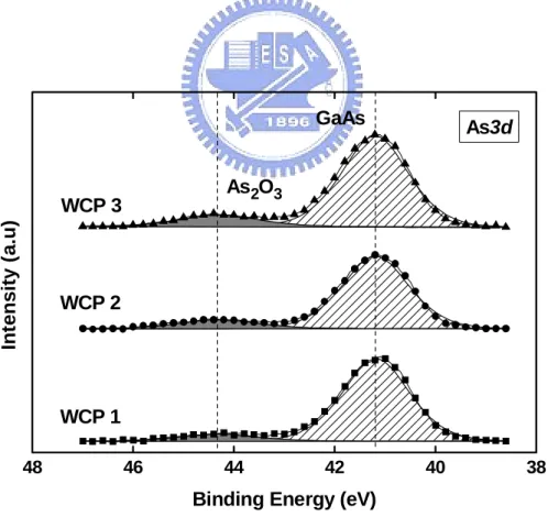
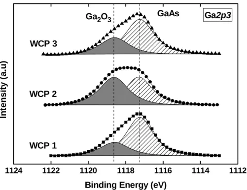
Table 2 shows the wet-chemical cleaning process (WCP) used in the study. We chose HCl and H2O2 mixture solution for our cleaning process. Figure 2-1 to 2-4 display the
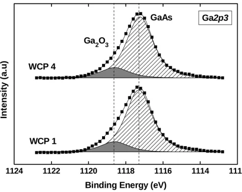
core-level spectra of As 2p3, As 3d, Ga 2p3, and Ga 3d for the GaAs substrates after WCP, respectively. The binding energies of As2O3, As-As (called As layer), and GaAs substrate
are 1326 eV, 1324.6 eV, and 1322.9 eV in As 2p3 spectrum, respectively. As figure 2-1 shown, it was observed that WCP 1 could suppress more As oxides than WCP 2. Moreover, As layer was less after WCP 1. From table 3, it could be pointed out more clearly. By using WCP 1, the ratios of Asoxide/AsGaAs and Aslayer/AsGaAs were 0.63 and 0.17, respectively.
Both of them were lower than by using WCP 2, and it meant that stronger concentration of HCl solution suppressed more As oxides and As layer, indeed. The binding energies of As2O3, As layer, and GaAs substrate are 44.3 eV, 41.9 eV, and 41.2 eV in As 3d spectrum,
respectively [34-37]. From As 3d spectrum as shown in figure 2-2, the same tendency happened to As oxides again. However, As layer existed the interfacial surface between native oxides and substrate rather than deep substrate. Thus, we could not find As layer in As 3d core-level spectrum. The binding energies of Ga2O3 and GaAs substrate are 1118.6
eV and 1117.2 eV in Ga 2p3 spectrum, respectively. In figure 2-3, the Ga2O3 intensity of
WCP 1 was lower than WCP 2. It could also be observed the same tendency in table 3. The Gaoxide/GaGaAs ratio of WCP 1 was 0.37 and lower than WCP 2. In Ga 3d spectrum, the XPS
spectrum is dominated by peaks at 20.6 eV and 19.2 eV which are assigned as Ga2O3 [38]
and GaAs substrate [39], respectively. We could observe the same situation in figure 2-4. In other words, stronger concentration of HCl solution suppressed more Ga oxides, indeed. As the mixture solution of HCl and H2O2, WCP 3, was employed, we found that WCP
3 would not be more effective against native oxides than WCP 1. As figure 2-1 to 2-4 and table 3 shown, it was observed the As oxides, As layer, and Ga oxides intensity of WCP 3 were all higher than WCP 1. It was because H2O2 oxidized the substrate resulting in oxides
increasing after WCP 3. Therefore, WCP 1 was the better of the three wet-chemical cleaning processes displayed in table 2.
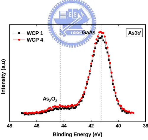
As above mentioned, WCP 1 which was used the stronger concentration of HCl solution and not mixed with H2O2 was more effective against native oxides. Thus, if we
employed much stronger HCl solution, WCP 4 as shown in table 4, the elimination of native oxides might be much better. From figure 2-5, the As oxides intensity of WCP 4 seemed to be higher than WCP 1, and in figure 2-7, there was the same tendency of Ga2O3.
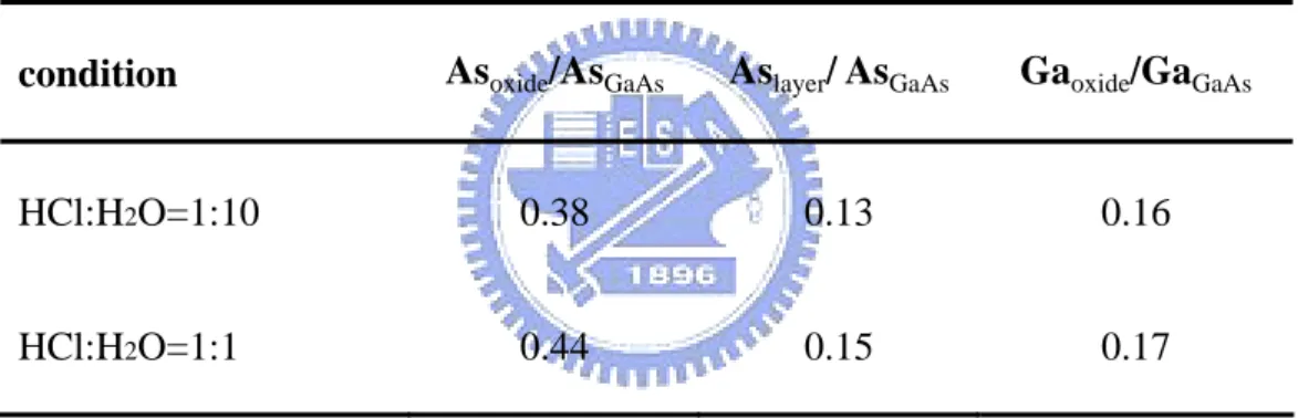
As figure 2-6 and 2-8 shown, we could not distinguish which cleaning process was better, because the GaAs substrate intensity was higher than As or Ga oxides in deep substrate by using not only WCP 1 but WCP 4. From table 5, it could be found that the ratios of Asoxide/AsGaAs, Aslayer/ AsGaAs, and Gaoxide/GaGaAs by employing WCP 4 were 0.44, 0.15, and 0.17,
effect of WCP 4 was worse than WCP 1, and WCP 4 could not suppress more native oxides in other words. Therefore, the concentration of HCl solution about 10% which we used in WCP 1 was the optimization of this study. One thing should be mentioned especially that the chemical ratios by employing HCl solution about 10% were all different from table 3 and 5. There were two reasons because we did not experiment at the same time and the XPS instrument might cause the error. In other words, the experiment was not repeatibale.
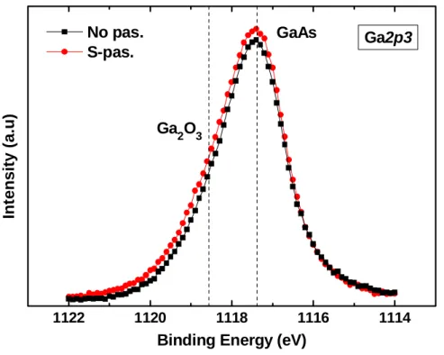
It is not enough to eliminate native oxides by only using HCl solution. Many researches have been reported that sulfide treatment could suppress the formation of native oxides, especially (NH4)2S solution. Therefore, (NH4)2S solution [40-44] about 1% was
used to passivate on the GaAs surface, after dipping in HCl solution about 10%. As figure 2-9 shown, we found that (NH4)2S treatment could eliminate more As oxides and As layer
than without treatment. From figure 2-10, it could be pointed out clearly that As oxides almost disappeared in deep substrate. However, nothing was different from with and without (NH4)2S treatment, from 2-11 and 2-12. This was because (NH4)2S solution
passivated on GaAs substrate could protect moisture against formation of native oxides. Thus, it was effective against native oxides to use (NH4)2S solution.
2-4 Summary
In this chapter, we studied different cleaning processes and different suppression effects of native oxides. It was found that about 10% was the optimization of the concentration of HCl solution for eliminating native oxides. More or less 10% HCl solution would decrease the cleaning effect resulting in the increasing of As oxides, As layer, and Ga oxides intensity. As the mixture solution of HCl and H2O2 was used, the
suppression of As and Ga oxides would be worse resulting from H2O2 oxidizing the
substrate. Thus, H2O2 would not be employed in our cleaning process. After dipping in HCl
solution about 10%, (NH4)2S solution about 1%, not the optimization, was used as a
Table 2 Wet-chemical cleaning processes (WCP) used in this study
WCP 1 WCP 2 WCP 3
DI. water rinse , 3 min DI. water rinse , 3 min DI. water rinse , 3 min
HCl:H2O=1:10 , 5min HCl:H2O=1:100 , 5min HCl:H2O2:H2O=1:1:10 , 5min
1330 1328 1326 1324 1322 1320 1318 WCP 1 WCP 2 As-As As2O3 GaAs As2p3 In te n s it y ( a .u)
Binding Energy (eV) WCP 3
Fig. 2-1 XPS spectrum As 2p3 after different cleaning processes of table 2
48 46 44 42 40 38 WCP 3 WCP 2 WCP 1 As2O3 As3d Int e nsit y ( a .u)
Binding Energy (eV) GaAs
1124 1122 1120 1118 1116 1114 1112 WCP 3 WCP 2 WCP 1 GaAs In te nsit y ( a .u )
Binding Energy (eV)
Ga2p3 Ga2O3
Fig. 2-3 XPS spectrum Ga 2p3 after different cleaning processes of table 2
24 22 20 18 16 Ga 2O3 WCP 1 WCP 2 WCP 3 In te n s it y ( a .u )
Binding energy (eV)
Ga3d GaAs
Table 3 Chemical ratio by XPS spectra of As 2p3 and Ga 2p3 according to different cleaning processes
condition Asoxide/AsGaAs Aslayer/ AsGaAs Gaoxide/GaGaAs
HCl:H2O=1:10 0.63 0.17 0.37
HCl:H2O=1:100 0.93 0.28 1.05
HCl:H2O2:H2O=1:1:10 0.83 0.24 0.46
Table 4 Wet-chemical cleaning processes (WCP) used in this study
WCP 1 WCP 4
DI. water rinse , 3 min DI. water rinse , 3 min HCl:H2O=1:10 , 5min HCl:H2O=1:1 , 5min
1330 1328 1326 1324 1322 1320 1318 1316 GaAs As-As As2O3 WCP 4 WCP 1 In ten sit y ( a.u )
Binding Energy (eV)
As2p3
Fig. 2-5 XPS spectrum As 2p3 after different cleaning processes of table 4
48 46 44 42 40 38 WCP 1 WCP 4 In ten sit y ( a.u )
Binding Energy (eV)
As3d GaAs
As2O3
1124 1122 1120 1118 1116 1114 1112 Ga2O3 GaAs WCP 1 WCP 4 Int e nsit y ( a .u )
Binding Energy (eV)
Ga2p3
Fig. 2-7 XPS spectrum Ga 2p3 after different cleaning processes of table 4
24 22 20 18 16 WCP 1 WCP 4 In ten sit y ( a.u )
Binding Energy (eV)
Ga3d GaAs
Ga2O3
Table 5 Chemical ratio by XPS spectra of As 2p3 and Ga 2p3 according to different cleaning processes
condition Asoxide/AsGaAs Aslayer/ AsGaAs Gaoxide/GaGaAs
HCl:H2O=1:10 0.38 0.13 0.16
1332 1330 1328 1326 1324 1322 1320 1318 In tensit y ( a.u )
Binding Energy (eV)
As2p3 GaAs As2O3 As-As no pas. S-pas.
Fig. 2-9 XPS spectrum As 2p3 of cleaning substrates with or without (NH4)2S solution
48 46 44 42 40 38 S-pas. no pas. In te nsit y ( a .u )
Binding Energy (eV)
As3d GaAs
As2O3
1122 1120 1118 1116 1114 No pas. S-pas. Int e nsity ( a .u)
Binding Energy (eV)
Ga2p3 GaAs
Ga2O3
Fig. 2-11 XPS spectrum Ga 2p3 of cleaning substrates with or without (NH4)2S solution
22 21 20 19 18 17 No pas. S-pas. Int e n s ity ( a .u )
Binding Energy (eV)
Ga3d GaAs
Ga2O3
Chapter 3
Atomic Layer Deposited Al
2O
3on GaAs
3-1 Introduction
As mentioned in chapter 1, there are more defects on the interface between high-k materials and GaAs substrate. Thus, we should use stable deposited mechanism to grow high quality films such that defects on interfacial layer could be decreased. Al2O3 deposited
by atomic layer deposition system (ALD) is just what we need. Al2O3 is a widely used
insulating material as gate dielectric, tunneling barrier and protection coating due to its excellent dielectric properties, strong adhesion to dissimilar materials, and its exceptional thermal and chemical stabilities. Al2O3 has a high band gap (~ 9 eV), a high breakdown
electric field (5-30 MV/cm) [45, 46], a high permittivity (8.6-10), high thermal stability (up to at least 1000o
C), and remains amorphous under typical processing conditions. The leakage current observed in ultrathin Al2O3 on GaAs is equivalent to or lower than that of
the state-of-the-art SiO2 on Si. The breakdown electric field of Al2O3 film thicker than 50 Å
can be up to ~ 10 MV/cm; this value is near the bulk breakdown electric field for SiO2.
ALD is an ultrathin film deposition technique based on sequences of self-limiting surface reactions, which enables thickness control on the atomic scale. The mechanism of ALD is like chemical vapor deposition (CVD), but it is step by step. However, AlO films
are grown by using alternating pulses of Al(CH3)3 (TMA, the aluminum precursor) and
H2O (the oxygen precursor) in the presence of N2 carrier gas flow. Its mechanism is as
figure 3-1 shown, and we call these processes one cycle. First, TMA is fed into the reactor and react with the OH bond on the GaAs substrate. Then, the reactor is purged with pure N2 gas to clean out products and residual TMA. Third, H2O is purged into the reactor and
forms Al2O3 on surface. Finally, the reactor is purged with pure N2 gas again to clean out
products and residual H2O. Step by step, Al2O3 films could be deposited layer by layer.
According to this characteristic, we could decrease voids for aspect ratio, as figure 3-2 shown.
3-2 Experimental Procedures
Metal oxide semiconductor (MOS) capacitors were fabricated on (100) oriented n-type Si doped GaAs wafers with a doping concentration of 1 x 10¹⁸
/cm3
. The optimized cleaning procedure which was mentioned in chapter 2 was used for GaAs wafers. Al2O3
films were deposited by ALD and Pt about 700 Å grown by sputtering was through a shadow mask to form the top gate electrode about 4 x 10⁻⁴
cm2
. The backside of GaAs substrate would be deposited a Al film about 3000 Å by thermal coater to reduce the contact and series resistances. As above mentioned, two challenges, suppressing native oxides and depositing excellent films, should be solved. We could passivate (NH4)2S
solution on GaAs surface to eliminate native oxides, and we had to find out the optimization. There is one heater in ALD system which is like CVD, and substrates could be deposited at different temperature. However, it should be found out the optimized temperature to grow excellent films on GaAs. The capacitance-voltage (C-V) and conductance- voltage (G-V) curves were measured using an HP4284 LCR meter, while the current-voltage (I-V) characteristics were measured using a Keithley 4200 semiconductor analyzer system. For physical analysis, characterization of the oxide composition was analyzed by X-ray photoelectron spectroscopy (XPS).
3-3 Results and Discussion
3-3-1 ALD Temperature optimization
To sure the optimized temperature, (NH4)2S passivation did not be used after cleaning.
We chose two kinds of temperature, 100o
C and 300o
C, to grow Al2O3 films by ALD.
Figure 3-3 (a) and (b) show capacitor multi-frequency C-V characteristics of MOS capacitors (Pt/Al2O3/n-GaAs) by ALD (60 cycles) at 100oC and 300oC, respectively. It
could be observed that the capacitance at 300o
C in the accumulation regime was higher than 100o
C. The growth rate at 100o
C was faster than 300o
C on Si, as shown in figure 3-4 [48]. Certainly, growth rate would be different from substrates and machines, but the same tendency. In other words, the AlO film deposited on GaAs at 100o
300o
C at the same cycles. Thus, thicker films resulted in lower capacitance and leakage current density, as figure 3-3 and 3-5 shown.
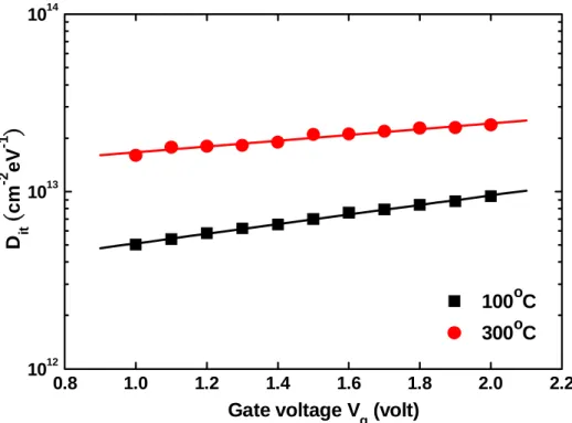
We had employed the conductance method [49] for more accurate estimate of the interface trap density (Dit). Figure 3-6 shows Dit vs. Vg at 100oC and 300oC. It can be seen
apparently that Dit at 300oC was higher than 100oC, which probably associated with poor
quality of the interfacial layer. However, it would be observed from figure 3-7 that the gate leakage current density (Jg) at 300oC was lower than 100oC at the same capacitance
equivalent thickness (CET). As table 6 shown clearly, Dit at 300oC was nearly one order
higher than 100o
C, but Jg (CET = 40 Å) at 300oC was three orders lower than 100oC. Thus,
considering the gate leakage current issues, 300o
C was chosen as the deposited temperature to grow ALD-Al2O3 on GaAs substrates.
3-3-2 Interfacial Passivation Layer on GaAs
Many researches have been reported that an interfacial passivation layer (IPL) could be added on the GaAs surface to eliminate native oxides which are not suppressed easily and to deposit excellent dielectric layer on GaAs. Two of IPLs are dipping in (NH4)2S
solution and capping one thin Si layer (called Si capping) [50-52]. Si capping was sputtered 10 Å by using a 4 in. Si target and 60 W dc power. In additional, the conditions of sulfide treatment were (NH4)2S(aq.) about 2% dipping 30s, 30m, and (NH4)2S(aq.) about
Figure 3-8 display C-V (10 kHz) curves of Pt/Al2O3/GaAs MOS capacitors with
different IPLs, and the Al2O3 film was deposited by ALD (300oC, 60 cycles). (NH4)2S(aq.)
passivation ( ~2%, 30s) was the best in this work, since the C-V characteristic which was dipped in (NH4)2S solution about 2% 30s showed sharper curve with higher accumulation
capacitance. This was indicated that (NH4)2S(aq.) passivation ( ~2%, 30s) was effective to
suppressed native oxides resulting in the gate dielectric constant increasing. However, the accumulation capacitance of Si capping was almost the same as control (without IPL), but the flat band shifted to negative voltage direction, which meant that positive traps formed by Si capping. From As 2p3 and Ga 2p3 XPS spectra, as figure 3-9 (a) and (b) shown, both of sulfide treatment and Si capping eliminated larger As and Ga oxides than without IPL. After sulfide treatment was done, we would like to know if As-S and Ga-S bonds formed on the surface, certainly. Figure 3-10 (a) displays that no As-S bond signal was on the interfacial layer between Al2O3 film and GaAs substrate. From Ga 3d core level spectrum
shown in figure 3-10 (b), the binding energy at 23.6 eV overlaps with O 2s core level [53]. In other words, Ga-O and Ga-S bonds signals could not be observed, but the Al-O bond signal could be pointed out at 23.6 eV. Moreover, since we used Al Kα X-rays to excite As
and Ga, S 2p and S 2s core level spectra, not shown, overlap with the Ga 3s peak and As LMM Auger peak [54], respectively. Thus, the sulfide treatment effect could not be understood from XPS spectra, directly.
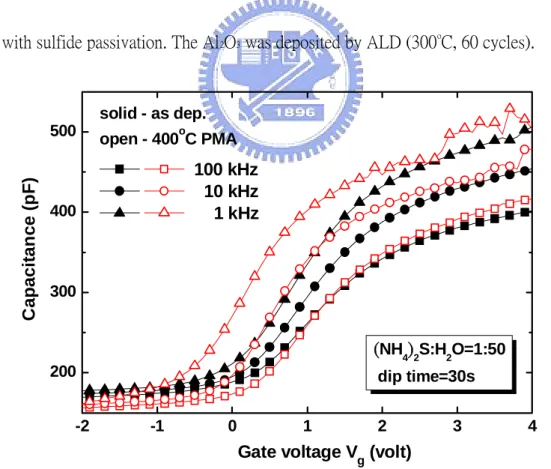
Figure 3-11 shows C-V characteristics of MOS capacitors (Pt/Al2O3/GaAs) without
(control) and with (NH4)2S passivation (~2%, dipped 30s), and the Al2O3 film was grown
by ALD (300o
C, 60 cycles). We could find that the accumulation capacitance with passivation were higher than without passivation at 100 kHz to 1 kHz. It was indicated that sulfide treatment was effective to improve the interface on the GaAs surface and made the Al2O3 films grown excellently. After Pt gate deposited by sputtering, post metallization
annealing (PMA) 60s in N2 atmosphere at 400oC was employed and this process attempted
to densify Pt gate. However, it was observed that the gate leakage current density (Jg) after
PMA increased such that the accumulation capacitance displayed abnormal curve at 1 kHz, as figure 3-12 shown. Figure 3-13 shows clearly that Jg increased after N2 PMA. This was a
different condition from Si which thermal process caused Jg increasing instead of being
better. Thus, it would be discussed in chapter 4.
Figure 3-14 (a) displays multi-frequency C-V curves characteristics of MOS capacitor without IPL (control). The interface state would influence frequency dispersion and hysteresis of MOS capacitor. Therefore, we employed ΔC and ΔV corresponding with the interface state density (Dit) [55]. ΔC and ΔV could be expressed as
(@1 kHz) (@100 kHz) (@1 kHz) C C C C − Δ = , (3.1) ΔV = V( @ 100 kHz C ) - V( @ 1 kHz C )FB FB , (3.2) where 1 1 1 FB ox DL C =C +C , (3.3)
CDL=1066 pF for GaAs, and Cox=1 kHz Cmax. From figure 3-14 (b), it would be observed
that ΔC and ΔV were lower after passivation. In other words, Dit was decreased by
passivation. Although dipping in (NH4)2S solution about 2% 30s did not result in the
lowest ΔC and ΔV, this method caused higher accumulation capacitance and sharper C-V curve than others. Thus, it was thought that (NH4)2S solution (~2%, dipping 30s) was better
method than others.
Certainly, it would be supposed that (NH4)2S solution diluted about 1% may be better
than 2%. As figure 3-15 shown, using 1% (NH4)2S solution resulted in the accumulation
capacitance lower than 2%. Figure 3-16 displays the ac loss (Gp/ω) vs. frequency for
different biases on Pt/Al2O3/GaAs MOS capacitors by ALD (300oC, 60 cycles) without IPL.
As conductance method was employed to calculate accurate the interface state density (Dit),
as figure 3-17 shown, it was observed that using sulfide passivation decreased Dit, and 1%
(NH4)2S solution was not more effective than 2%. After ALD-Al2O3, the film was annealed
at 600o
C with O2 60s in the rapid thermal annealing chamber and attempted to be densified.
However, Dit and the gate leakage current density (Jg) increased again after thermal
treatment, as figure 3-18 and 3-19 display. Thermal process might not be treated on ALD-Al2O3/GaAs. It could be sure that dipping in 2% (NH4)2S solution 30s is the
3-4 Summary
In this chapter, we discussed how to improve the interfacial layer between Al2O3 and
GaAs surface. First, the optimization ALD-Al2O3 deposition temperature had to be tried,
and 300o
C was the best for growing excellent Al2O3 film, considering the leakage current
issues. Then, the native oxides could be suppressed by interfacial passivation layer (IPL) before depositing Al2O3 films, and (NH4)2S passivation and Si capping were two better
choices of IPLs. However, it was found that dipping in 2% (NH4)2S solution 30s resulted in
larger accumulation capacitance, sharper C-V curves, and lower Dit than others. Thus, it
was supposed that dipping in 2% (NH4)2S solution 30s was the optimization for eliminating
native oxides and growing excellent Al2O3 films. Summarizing the Al2O3/GaAs fabrication
process, we would clean the GaAs wafers by the method mentioned in chapter 2 first, then dip the wafers in the 2% (NH4)2S solution about 30s, and finally deposit Al2O3 at 300oC by
Fig. 3-1 Atomic layer deposition (ALD) reaction mechanism
-3 -2 -1 0 1 2 3 4 100 120 140 160 180 200 100 kHz 10 kHz 1 kHz 100oC dep. temp. C a pacitan ce ( p F)
Gate voltage Vg (volt)
(a) -3 -2 -1 0 1 2 3 4 100 200 300 400 100 kHz 10 kHz 1 kHz 300oC dep. temp. C a pa c it a nc e (p F )
Gate voltage Vg (volt)
(b)
Fig. 3-3 Multi-frequency C-V characteristics of MOS capacitors (Pt/Al2O3/GaAs) by ALD
(60 cycles) at (a) 100o
C (b) 300o
Fig. 3-4 Growth rate of different surface temperature (K) on Si [48] 0.0 0.5 1.0 1.5 2.0 2.5 3.0 10-10 10-9 10-8 10-7 10-6 10-5 10-4 Gate voltage V g (volt) G a te leakage Jg ( A/ c m 2 ) 100oC 300oC
Fig. 3-5 The effect of temperature on J-V characteristics of Pt/Al2O3/GaAs MOS capacitor
0.8 1.0 1.2 1.4 1.6 1.8 2.0 2.2 1012 1013 1014 D it
(
cm -2 eV -1)
Gate voltage V g (volt) 100oC 300oCFig. 3-6 Dit vs. Vg characteristics of Pt/Al2O3/GaAs MOS capacitor made by ALD (60cycles)
at 100o C and 300o C 10 20 30 40 50 60 70 80 90 10-10 10-8 10-6 10-4 10-2 100
300
oC
G ate leak ag e J g @ V g = 2V ( A/ c m 2 ) CET(
Angstrom)
ALD-Al2O3/GaAs100
oC
Table 6 Average of Dit and Jg at CET = 40 Å of Pt/Al2O3/GaAs MOS capacitor made by ALD at 100o C and 300o C ALD-Al2O3 Dit (cm-2eV-1) Jg (A/cm2) 100o C 7 x 10¹² 2 x 10⁻⁴ (CET = 40Å) 300o C 2 x 10¹³ 1 x 10⁻⁷ (CET = 40Å) -3 -2 -1 0 1 2 3 4 100 200 300 400 500
Gate voltage Vg (volt)
control Si cap. 1:50, 30s 1:50, 30m 1:10, 30s C a pacit a n ce ( p F ) Freq.=10 kHz
Fig. 3-8 C-V (10 kHz) curves of Pt/Al2O3/GaAs MOS capacitors with different IPLs. The
1332 1330 1328 1326 1324 1322 w/o IPL Si cap. Sulf.(aq.)=1:50, 30s As2O5 As2O3 As2p3 In te n s ity ( a .u)
Binding Energy (eV) (a) 1126 1124 1122 1120 1118 1116 1114 w/o IPL Sulf.(aq.)=1:50, 30s Si cap. In te nsit y ( a .u )
Binding Energy (eV)
Ga2p3
Ga2O3
(b)
44 42 40 38 w/o IPL 1:50 30s Si cap. GaAs As3d In te n s ity ( a .u)
Binding Energy (eV) (a) 28 26 24 22 20 18 16 w/o IPL 1:50 30s Si cap. GaAs Ga3d In te nsity ( a .u)
Binding Energy (eV) overlap with O2s
(b)
-2 -1 0 1 2 3 4 100 200 300 400 500 (NH4)2S:H2O=1:50 dip time=30s 100 kHz 10 kHz 1 kHz C a pa c ita n c e (p F ) Gate voltage V g (volt) solid - control open - sulfide
Fig. 3-11 Multi-frequency C-V characteristics of MOS capacitors (Pt/Al2O3/GaAs) without
and with sulfide passivation. The Al2O3 was deposited by ALD (300oC, 60 cycles).
-2 -1 0 1 2 3 4 200 300 400 500 (NH4)2S:H2O=1:50 dip time=30s 100 kHz 10 kHz 1 kHz C a pacit a n ce ( p F) Gate voltage V g (volt) solid - as dep. open - 400oC PMA
Fig. 3-12 C-V curves of Pt/ Al2O3/GaAs capacitors before and after 400oC PMA. The Al2O3
was deposited by ALD (300o
10-8 10-6 10-4 10-2 100 C u rr en t d e ns ity J g @ V g = 2V ( A/ c m 2 ) as-dep. 400oC N2 PMA Sulf.(aq.) 1:10, 30s Sulf.(aq.) 1:50, 30m Sulf.(aq.) 1:50, 30s
Si cap.
control
Fig. 3-13 Jg versus different IPLs for Pt/Al2O3/GaAs MOS capacitors made by ALD (300oC,
-3 -2 -1 0 1 2 3 4 100 200 300 400 100 kHz 10 kHz 1 kHz control C a pacitan ce ( p F) Gate voltage V g (volt) CFB = 299 pF Δ
C
ΔV
(a) 15 20 25 30 35 0 1 2 3passivation
ΔV
(v
ol
t)
ΔC (
%
)
Sulf.(aq.) 1:50, 30m Sulf.(aq.) 1:50, 30s Sulf.(aq.) 1:10, 30s Si cap. control as depesited (b)Fig. 3-14 (a) C-V characteristics of Pt/Al2O3/GaAs MOS capacitors without IPL and (b) ΔC
and ΔV versus different IPLs by ALD (300o
-3 -2 -1 0 1 2 3 4 100 200 300 400 500 Freq.=10 kHz w/o IPL 1:50, 30s 1:100, 30s C a pa c ita n c e (p F )
Gate voltage Vg (volt)
Fig. 3-15 C-V (10 kHz) curves of Pt/Al2O3/GaAs MOS capacitors with different IPLs. The
103 104 105 0.0 0.4 0.8 1.2 1.6 2.0 2.0 V Frequency (Hz) 1.0 V Vg = 1.0 V to 2.0 V, step: 0.2 V G p / ω ( μ F/cm 2 ) control
Fig. 3-16 Plot of the ac loss (Gp/ω) vs. frequency for different biases on Pt/Al2O3/GaAs
MOS capacitors by ALD (300o
C, 60) cycles without IPL
1.0 1.2 1.4 1.6 1.8 2.0 1012 1013 1014
D
it(
cm
-2eV
-1)
Gate voltage V
g(volt)
control (NH4)2S:H2O=1:50 (NH4)2S:H2O=1:100Fig. 3-17 Interface state density (Dit) as a function of gate voltage for MOS capacitors
1012 1013 1014 (NH4)2S : H2O = 1 : 100 (NH4)2S : H2O = 1 : 50 control as-dep. 600oC O2 PDA D it
(
cm -2 eV -1)
Fig. 3-18 Dit versus different IPLs for MOS capacitors Pt/Al2O3/GaAs made by ALD
(300o C, 60 cycles) 10-7 10-6 10-5 10-4 10-3 10-2 10-1 100 as-dep. 600oC O2 PDA G a te le ak ag e J g @ V g = 2 V ( A/ c m ) 2
)
(
NH4)
2S : H2O = 1 : 100(
NH4)
2S : H2O = 1 : 50control
Fig. 3-19 Gate leakage current density versus different IPLs for Pt/Al2O3/GaAs MOS
capacitors made by ALD (300o
Chapter 4
Thermal Effect of Al
2O
3/GaAs by ALD
4-1 Introduction
Silicon has been used in COMS technology for decades due to better qualities of its native oxides such as low interface state density and good thermal stability. But, with further downscaling device dimensions and the shrinkage of gate oxide thickness to nanometer range, the leakage current density of SiO2 is too large to be accepted.
GaAs-channel devices which including bulk GaAs and strained GaAs with the integration of high-k gate dielectrics have gained considerable research interest. Some materials which have high dielectric constant are introduced to suppress excessive leakage concern with a thicker physical thickness while still maintaining the capacitance equivalent thickness (CET) of the scaled devices. Up to the present, Al2O3 deposited by atomic layer deposition
system (ALD) are the uppermost candidate among all potential high-k dielectrics. All of Si, Ge and GaAs metal oxide semiconductor field effect transistors (MOSFETs) with high-k gate dielectrics have shown come promising performances [56, 57]. Our work presents the electrical characteristics of Al2O3 thin films deposited on GaAs substrates. Moreover, the
gate leakage current after annealing increased as mentioned in chapter 3. Thus, the effect of thermal processing on entire capacitor structures has to be also studied.
4-2 Experimental Procedures
The GaAs substrates were used (100) Si doped n-type wafers with a doping concentration of 1 x 10¹⁸
/cm3
. The wafers were subjected to the cleaning process of DI. water rinse 3 minutes, followed by diluted HCl solution (1:10) dipping 5 min, and DI. water rinse 3 minutes again. The wafers were dipped in 2% (NH4)2S solution about 30s to
eliminate native oxides. After dried by N2 gas, the Al2O3 films were deposited by ALD at
300o
C. The films were annealed at 600o
C with O2 [45, 58] or N2 1 minute in the rapid
thermal chamber and attempted to be better. Pt gate about 4 x 10⁻⁴
cm2
through a shadow mask was sputtered 700 Å with 45 W dc power, and 400o
C N2 post metallization annealing
(PMA) was employed to densify the metal gates. Finally, Al was deposited by thermal coater on the backside of GaAs wafer to reduce the contact and series resistances. The high resolution transmission electron microscope (HRTEM) technique by JEM-2100F was taken to characterize the crystallinity and interfacial structure of Al2O3 films. The chemical
composition and the state of elements were further analyzed by XPS. A 1486.6 eV Al Kα
radiation source was used for excitation. The capacitance-voltage (C-V) and conductance- voltage (G-V) curves were measured using an HP4284 LCR meter, while the current-voltage (I-V) characteristics were measured using a Keithley 4200 semiconductor analyzer system.
4-3 Results and Discussion
4-3-1 Electric and Physical Characteristics
Figure 4-1 displays C-V curves at 10 kHz of MOS capacitors (Pt/Al2O3/GaAs) with
and without O2 600oC PDA. It could be pointed out that the accumulation capacitance after
O2 600oC PDA 60s was higher than without PDA. It was supposed that as O2 600oC PDA
was employed, O2 reacted with Al2O3 and filled the dangling bonds at high temperature
resulting in increasing the dielectric constant of Al2O3 film and densifying the film.
However, it was found that the capacitance after PDA in the accumulation regime was not saturated but upping. This might be affected by larger leakage current. As figure 4-2 shown, the hysteresis after PDA was smaller than without PDA. It was thought that high temperature caused the traps in the depletion regime lowing such that hysteresis decreased. Although capacitance increased and hysteresis decreased after O2 600oC PDA, the leakage
current which we concerned mostly increased instead, as figure 4-3 shown.
Figure 4-4 displays multi-frequency C-V characteristics of MOS capacitors (Pt/Al2O3/GaAs) with O2 and N2 600oC PDA, and the Al2O3 film was deposited 100 cycles
by ALD at 300o
C. After O2 PDA, the accumulation capacitances at 100 kHz to 1 kHz were
all higher and sharper than N2. Moreover, the flat band all shifted to negative voltage, and
it was meant that the positive traps formed after O2 PDA. However, it could be observed
affected by larger leakage current. As the Al2O3 films was shrunk to 60 cycles, as figure
4-5 shown, the C-V curves with O2 PDA were all larger and sharper. However, the curves
after N2 or O2 PDA at 1 kHz were both affected by larger leakage current. From figure 4-6,
it was pointed out that high temperature resulted in the traps in the depletion regime lowing such that hysteresis decreased. Moreover, it was also found that the hysteresis after O2
PDA was smaller than N2 because O2 filled the dangling bonds in the Al2O3 films. Figure
4-7 shows that the leakage current with N2 PDA was larger two orders than O2.
Nevertheless, the leakage current with O2 PDA was not ignored, indeed.
Figure 4-8 displays the HRTEM cross-sectional image of 100cycles Al2O3 film with
N2 PDA on GaAs substrate. A uniform, continuous, and amorphous Al2O3 film was
observed, and its thickness was about 9.2 nm. The interface between Al2O3 and GaAs
substrate was clear, and the interfacial layer on GaAs surface could be observed. As mentioned above, O2 might fill and densify the Al2O3 film. Thus, as figure 4-9 shown, the
Al2O3 film with O2 PDA was blear and thinner than N2. Moreover, the film after O2 PDA
was damaged easily by focused ion beam (FIB) such that the orientation of substrate surface was not clearer than N2. However, it could be pointed out less interfacial layer
between Al2O3 and GaAs substrate than N2. As the Al2O3 film with O2 PDA was shrunk, it
could be also observed the blear and damaged film as figure 4-10 shown. According to physical thickness by TEM, CET vs. physical thickness graph could be obtained, as figure
4-11 shown. As mentioned that O2 could fill the Al2O3 film and make the dielectric
constant larger, it was demonstrated through figure 4-11. Moreover, the interfacial layer which O2 PDA made was thinner than N2.
Figure 4-12 displays leakage current density (Jg) vs. capacitance equivalent thickness
(CET) graph for Pt/Al2O3/GaAs MOS capacitors with O2 and N2 600oC PDA. It was
observed that Jg caused by N2 PDA was higher than O2 at the same CET. As thermal
process was treated on MOS capacitor of GaAs, the leakage current which we concerned mostly would increase, especially after N2 PDA or PMA. It had been demonstrated by XPS.
As PDA was employed on Al2O3 film, the substrate would produce As and As bonding
resulting in forming As cluster (called As layer). This chemical reaction at high temperature could be expressed
As2O3 + 2GaAs → Ga2O3 + 4As [59].
The product, 4As, was which was called As layer. The metallic As was incorporated into the Al2O3 film [60], creating trapping centers. Accordingly, As layer caused electric
conduction paths [61, 62] to result in larger leakage current. From figure 4-13, it was found that As layer after N2 PDA was more than others. In the upper chemical reaction, it was
known that as GaAs intensity was stronger, the reaction would speed up and produce more Ga2O3 and As layer. In figure 4-13, Ga 2p3 spectrum, it could be observed Ga2O3 intensity
7 that the AsGaAs/Asoxides ratio after N2 PDA was 6.65 larger than others and N2 PDA reacted
more As layer such that Aslayer/Asoxides ratio was 22.3, the highest value in the three
conditions. However, N2 PDA treated on the Al2O3 film was thicker than O2 from TEM. In
other words, it was supposed that N2 PDA made the GaAs substrate out-diffusion such that
the GaAs intensity in the Al2O3 film was higher than O2 resulting in more As layer and
increasing leakage current. In sum, PDA would cause As layer and N2 atmosphere would
make more GaAs diffusing into Al2O3 films than O2 such that the chemical reaction sped up.
Thus, the leakage current after N2 PDA was larger than O2.
4-3-2 Reliability Issues
Reliability is one of the most important issues of high-k material for practical application in electronic product. Thus, it was discussed that sulfide treatment (dipping in (NH4)2S solution ~2% 30s) and PDA affected reliability. Figure 4-15 show the leakage
current density (Jg) as a function of stress time after constant voltage stress (CVS). At CVS
Vg=4.5V, as figure 4-15 (a) shown, the leakage current density (Jg) with N2 PDA was the
largest in the three conditions certainly. Although Jg of O2 PDA + sulf. was larger than O2
PDA, Jg of O2 PDA increased faster than others with stress time increasing such that the
slope of O2 PDA was the sharpest. As the gate bias was added to 5V, it could be found that
the slope of O2 PDA was also the sharpest, as figure 4-15 (b) shown. Thus, it was