A Novel Device Structure for Low-Temperature Polysilicon TFTs with
Controlled Grain Growth in Channel Regions
Li—Jing Cheng, Yin-Lung Lu, Ching-Wei Lin, Ting-Kuo Chang and Huang-Chung Cheng
Institute ofElectronics, National Chiao Tung University, Hsinchu, 300 Taiwan
ABSTRACT
in this paper, we demonstrate a novel device structure of low-temperature polysilicon thin-film transistors (LTPS TFTs) for AMLCD applications with using excimer-laser crystallization (ELC). The device structure consists of a thin channel and a thick source/drain. This structure has its merit in the process of ELC and is capable of improving TFTs' electrical characteristics. During excimer laser irradiation, this kind of recessed structure is able to build up localized lateral thermal gradients in the regions near the steps and entice crystallization from the chillerthick source/drain regions toward the hotter thin channels. Because ofthe development of crystallization process, the average field-effect mobility ofthe devices can be increased to about 350 cm2fV.s, and the on/off current ratios exceed eight orders. In addition to improvement of device performance, the process window ofELC is broadened with the recessed structure.
Keywords: low-temperature polysilicon thin-film transistors (LTPS TFTs), excimer-laser crystallization (ELC), recessed channel, localized lateral thermal gradient
INTRODUCTION
Low-temperature polycrystalline silicon thin-film transistors (LTPS TFTs) have been studied because oftheir potential application in high-performance active matrix thin-film displays on glass substrate. Development of high-performance LTPS TFTs will benefit the cost-effective manufacturing of large-area active matrix liquid-crystal displays (AMLCD) by replacing the off-board driver circuits, thereby paving the way for future "system on glass" (SOG) or even "3-D integration" applications. Excimer-laser crystallization (ELC) is a powerful technology to produce high-quality polycrystalline silicon film with low thermal budget. However, as many prior literatures have shown, the gram size of the ELC polysilicon film is significantly dependent on energy density of laser irradiation. In addition, the energy for producing super-large grains is too critical to hit it right. In order to broaden the process window of ELC and improve crystal uniformity or even control the large grains in specific locations, especially in channels, we should apply some auxiliary method to reduce the sensibility of crystallized grain size to laser energy density and to direct gram growth. Lots of techniques on this issue have been discussed, such as ELC with pre-patterned Si films, with anti-reflective capping patterns or with shield masks. In this work, we have developed an alternative approach to control gram growth by using different thicknesses of x-Si silicon film. When pulsed laser irradiates the a-Si thin film with different thicknesses, the temperature in thin regions will ramp and quench more swiftly than the thick will do. Consequently, the lag of solidification in thin regions generates lateral thermal gradients and obliging grains to grow from the thick films to the thin. Here we tailor the thick silicon regions for source/drain and the thin for channels in order to make grains grow form the source/drain to the channel. Because stronger thermal gradients exist in the films with greater difference in thickness, the grains in the channel regions with thicker source/drain can extend longer. The gram configuration makes devices have low leakage current and high mobility. Importantly, the recessed-channel structure can be used to blunt the sensibility of grain size to applied laser energy, especially in small-dimensional devices.
EXPERIMENTAL
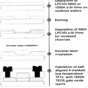
The process, illustrated in Fig. 1, starts with forming a-Si silicon films of 500A and 1000A individually on two oxidized wafers by LPCVD at 550°C with silane source. Next, we remove the a-Si silicon films at the channel regions and then deposit another 500A a-Si silicon films to form recessed-channel structures. The recessed structures consist of 500A channel regions and 1000 or l500A sources/drains. After excimer laser irradiation at 400°C, the crystallized silicon films are used to fabricate general self-aligned four-masked TFTs with 1000A TEOS gate oxide. The maximum temperature of all
InDisplay Technologies Ill, I-Wei Wu, Heiju Uchilke, Editor, 51
Proceedings of SPIE Vol. 4079 (2000) • 0277-786X1001$15.OO
52
processes is 600°C. Finally, some devices are passivated by NH3 plasma treatment at 300°C for four hours. In order to prove our prediction, we have observed the results of grain growth at the channels by SEM micrographs and compared the electrical characteristics of ELC recessed-channel TFTs with that of the conventional structure in different laser energy densities.
RESULTS AND DISCUSSIONS
Narrow process window ofELC harms the uniformity of TFTs' electrical characteristics. We ascribe this poor result to super lateral growth (SLG) phenomenon [1] appearing at a critical laser energy density irradiation. Laser energy fluctuation makes grains randomly grow from the residual nucleation sites at the silicon-oxide interface. More importantly, if a laser source with fixed energy density is applied, the number of the residual nucleation sites is predominately dependent on the thickness of silicon films. So the uniformity of film thickness and laser energy density becomes a potent influence on the uniformity of device performance. However, if the different thicknesses of silicon film are fabricated artificially, lateral thermal gradients can be generated after laser irradiation. By doing so, the residual nucleation sites can be controlled in the thick regions ifthe laser energy exceeds a level that is able to completely melt the thin regions.
Fig. 2 shows a simulation result of temperature profile after 3Ons-pulsed laser irradiation in a step silicon structure formed on an oxide substrate. We can find that lateral thermal gradient exists near the step region, while homogeneous nucleation resulting from completely melting dominates the crystallization process in the region far from the step. The result also tells us that the homogeneous grain growth will eventually hinder lateral growing grains if the recessed regions are too long. But ifthe solid-liquid interface laterally moves swifter, it is likely to overcome the homogeneous nucleating grains and stretch longer into the channels. Therefore, the strength of thermal gradient determinates the ability of lateral growth. By increasing the difference of film thickness, we can build up stronger lateral thermal gradients to enhance lateral grain growth. The SEM micrographs shown in Fig. 3 are good evidences to corroborate our idea to control grain growth in channel region with recessed structure. We observe that the grains can extend to about O.9prn from the two sides, 1 000 A source/drain regions, toward the center of 500A channel region, and the grains in recessed film with 1 500A source/drain can
stretch to about 1 5p.m.
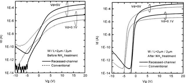
Fig. 4 shows Id-Vg curves of recessed-channel and conventional TFTs with 2p.m channel length before and after NH3 plasma treatment. We can see that the device performance of ELC recessed-channel TFTs is superior to that of the conventional. The recessed-channel TFTs display greater on-current and field-effect mobility; furthermore, minimum-current and subthreshold swing are lower either after or before plasma treatment. In our opinion, the higher field-effect mobility and lower subthreshold swing result from better crystallinity and the longitudinal grain growth in the channel regions. Additionally, since the extending grains have less intra-grain defects near drain junctions, the leakage current, which results from thermionic field emission tunneling mechanism [2], can be suppressed in the recessed-channel TFTs. The typical electrical characteristics of recessed-channel (black) and conventional TFTs before and after plasma treatment
are listed in Table 1.
Fig. 5exhibitsthe influence of channel length on ELC recessed-channel TFTs. The recessed structure shows its merit in improving device performance especially when the channel length is getting shorter. Beside, it is thanks to lateral thermal gradients occurring in the recessed structure that we can insensate the effect of laser energy density upon grain size. Fig. 6 tells us that if the applied laser energy density is greater than a critical level that makes the SOOA channel regions
completely melted (referring to the data of the conventional 500A-thick TFTs), the device performance is about the same. The reason is that during higher-energy laser irradiation, all of the silicon residual nucleation sites disappear in the channel regions. When lateral grain growth can be artificially controlled in the process of crystallization, the process window of ELC will be broadened.
CONCLUSION
Recessed-channel TFTs fabricated by using ELC have shown superior device performance to the conventional. With this kind of structure for ELC, higher field effect mobility, lower subthreshold swing and lower minimum-current can be obtained. We attribute the results to longitudinal grain growth along the channels and lower intragrain defects near drain junctions. Furthermore, the process window can be broadened, because lateral grain growth is artificially controlled in the process of crystallization.
REFERENCE
1 James S. Im and H. J. Kin, AppI. Phvs. Let!.. vol. 64, p. 2303, 1994.
[21 l.-W
Wu.A.G Lewis, T.-Y Iluang. W.B Jackson, and A Chiang. Electron Devices Meeting, 1990. Technical Digest.. International ,p.867 , 1990.Deposition of
LPCVD 500A or
I000A a-Si films on
oxidized wafers
Etching
Deposition of 500A
LPCVD a-Si filmsfor recessed
channels
Excimer laser
irradiation
Fabriation of
self-aligned 4-maskedlow-temperature
TFT5 with I000A
TEOS gate oxide layers
iOOflA
'.'
-. 5O0.
5-. - --. 720 nm (a) (b)Fig. 3 The SEM micrographs of Secco etched ELC recessed-structure silicon films.
(a) Grains extend about 0.9 J.m from the two sides, 1000 A source/drain regions, toward the center of SOOA channel region. (h) Grains extend about I .51.tm from the left side, 1500 A source/drain region, toward the right, 500A channel region
t. ..--....--
____
Excimer laser irradiation
Fig. I The brief process flow of recessed TFTs.
Fig. 2 Simulation of a temperature profile, in Kevine
degree, at the edge of a recessed silicon film aler
laser irradiation. The upper region above zero is
silicon and the bottom, silicon dioxide.Typical electrical characteristics of recessed-channel (black) and conventional TFTs before and after plasma treatment.
PEE on/off Vth (V) SS
(cm2N.s) @Vd=5V (mV/dec) 2p
With plasma 158 8E8 -3.26 270 treatment 156 3E8 -3.28 312 Without 2p
I •AII
74.3 5E5 1.71 2620 plasma treatment 5p 48.9 4E7 2.0 2460 V 1 E-4 1E-6 1E-8 V 1E-lO 1E-12 1E-14 -10 -5 Vg (V)Fig.4 Id-Vg curves of 2-tm recessed and conventional TFTs before (left) and after (right) NH3 plasma treatment. TABLE 1 0 5 10 15 20 Vg (V) 400 11:300 200 E C) 100
U-0
After NH3 plasma treatment
I I
. Recessed lETs
0
ConventionalTFTsAfter NH3 plasma treatment
I
I 400 C') 300>
0 200
E C.) a) 100U-0
.
2
5 10 Channel length (pm)Fig.5 Thecomparison of field-effect mobilities of recessed and conventional TFTs with different channel lengths.
Conventional TFTs
54
220 250 280 310 340
Laserenergy density (mJ/cm2)
Fig.6 The comparison of field-effect mobilities of recessed and conventional TFTs prepared with different laser energy densities.