Optical and electrical investigations of isoelectronic In-doped GaN
films
C.K. Shu*, W.H. Lee, Y.C. Pan, C.C. Chen, H.C. Lin, J. Ou, W.H. Chen, W.K. Chen,
M.C. Lee
Department of Electrophysics, National Chiao Tung University, Hsinchu, Taiwan, 300, ROC
Received 20 August 1999; accepted 19 December 1999 by Z.Z. Gan; received in final form by the Publisher 27 January 2000
Abstract
The optical and electrical properties of isoelectronic In-doped GaN films grown by metalorganic vapor phase epitaxy (MOVPE) were investigated by X-ray, photoluminescence (PL), Hall and Raman measurements. As a result, adequate In-doping quantity causes not only a reduction of yellow luminescence and unintentional background concentration, but an enhanced mobility and decrease in the widths. The improved crystalline and optical qualities of GaN films may be attributed to the decrease in defects.䉷 2000 Elsevier Science Ltd. All rights reserved.
Keywords: C. Impurities in semiconductors; D. Optical properties; D. Phonons; E. Luminescence
Although the optoelectronic applications of the group III-nitride materials have progressed rapidly, because of great improvements on film quality in terms of carrier mobility, dislocation density and deep levels, it is still challenging to obtain high quality samples [1–3]. It is known that the isoelectronic doping in conventional semiconductors was useful to enhance the optical and electrical properties. For example, N-doping had increased the quantum efficiency of GaP by approximately two orders of magnitude, and In-doping in GaAs had achieved the reduction of dislocation density by more than one order of magnitude [4–6]. However, there appears so far no thorough investigation of isoelectronic doping effects on group III-nitrides [7]. In our first attempt [8], we examined the In-doped GaN films that were grown on a 600 buffer layer at 1000⬚C and observed the improved optical flatness, but the optimal doping level and electrical property had not been deter-mined yet. In the present work, we have extended the In-doping level to two times higher and applied on better qual-ity samples in order to check whether there is any further improvement. As a result, we obtained an optimum con-dition under which the defect-related yellow luminescence (YL) was suppressed and the minimum carrier concen-tration and maximum mobility were achieved as well.
Our GaN film samples of⬃1.2 mm thick were grown on a (0001) sapphire substrate at 1035⬚C by metalorganic vapor phase epitaxy (MOVPE) [9]. Prior to top layer growth, a 350 GaN buffer layer was deposited at 525⬚C for strain relaxation. We fixed the flow rates for ammonia and trimethylgallium (TMGa) at 0.7 standard liter per minute and 10.3mmol min⫺1, respectively. For isoelectronic doping, we added trimethylindium (TMIn) at various flow rates from 0 to 4.4mmol min⫺1. This series of samples shows relatively weaker YL, larger I2 and higher
trans-parency than the previous series of samples. The crystalline structure and optical property of the as-grown films were first measured by double crystal X-ray diffraction rocking curve (XRC), Raman scattering and photoluminescence (PL) utilizing the systems described previously [10]. Then, by the Hall measurements, we determined the carrier concentration and mobility.
The influence of isoelectronic doping on the optical prop-erties of GaN is shown by PL spectra in Fig. 1. They all have the dominant I2peak at 358 nm and two weak features at 366
and 377 nm that are associated with the I3and
donor–accep-tor pair (DAP) transitions [11]. Since the YL is very weak, it is enlarged by 200 times and yet shows no multiple inter-ference effect that may be due to non-flat surface. As the TMIn flow rate increased, the I2 intensity dropped off
rapidly by a factor of ⬃40 and the YL reduced almost to zero. It is similar to Si-doped GaN [12], that the PL intensity
Solid State Communications 114 (2000) 291–293
SSC 5149
0038-1098/00/$ - see front matter䉷 2000 Elsevier Science Ltd. All rights reserved. PII: S 0 0 3 8 - 1 0 9 8 ( 0 0 ) 0 0 0 3 7 - 5
PERGAMON
www.elsevier.com/locate/ssc
decreases with the decreasing dopant concentration (refer to Fig. 2(b)). Apparently, the In-incorporation of proper amount can reduce the background concentration by compensating dislocations such that the radiative transitions are diminished [13]. Since the surface migration rate of In is higher than that of Ga, In may occupy the Ga site and form the radiation killers [14]. So far, no PL report for InN has appeared yet, probably because In atoms play as lumines-cence killers. The reason for such radiation quenching is still unknown and needs more studies. However, too much incor-poration of In atoms caused film deterioration, just like that of In over-doped GaAs and GaP [4–6].
Since the line width is due partly to the structural defects (such as dislocations, and vacancies VN and VGa, we thus
show the full-widths-at-half-maximum (FWHM) of the I2
and XRC (0002) peaks in Fig. 2(a). They resemble each other and both approach a minimum under a flow rate about 3mmol min⫺1. It reveals that the crystalline and opti-cal properties had been improved to some extent. We also notice that the film is indeed more transparent than those under flow rates below 2.8 and above 3.3mmol min⫺1. For comparison, the Hall mobility and concentration are also plotted in Fig. 2(b). As the flow rate increased to 2.8mmol -min⫺1, the mobility was enhanced and the concentration lowered. These trends are reversed for further increase in flow rate. The optimal electrical property occurs again under a flow rate about 3mmol min⫺1that is consistent with the XRC and PL results. In conventional III–V materials, the
background concentration often increases with the extrinsic impurity doping and the mobility decreases due to degraded lattice scattering. For n-type GaN, the prevailing dislo-cations introduce acceptor centers that will capture electrons to form negatively charged dislocations [15]. These will scatter electrons and cause mobility to decrease that may apply to our samples under the flow rates of 4.4 and less than 2.2mmol min⫺1.
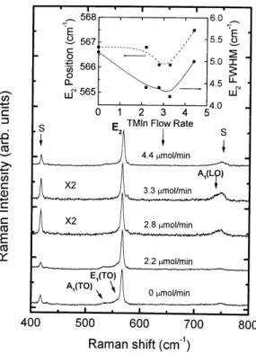
The Raman spectra of all our samples clearly show the hexagonal E2mode at 566 cm⫺1in Fig. 3 that confirms no
alloy formation by isoelectronic doping up to 4.4mmol -min⫺1. If the strain-free E2mode is at 568 cm⫺1, all films
are subjected to the tensile stress from 0.1 to 0.24 GPa [16]. For the undoped and In-doped films (under 2.2mmol -min⫺1), the E2line shape appears asymmetric that is resulted
from a combination of E1(TO) and A1(TO) features at 559
and 534 cm⫺1. This indicates the presence of partially mixed grain orientations that is manifested by the large diffused scattering. For those prepared under the TMIn flow rates of 2.8 and 3.3mmol min⫺1, they look more transparent as revealed by the larger signals from sapphire substrate. Now, both TO modes become unobservable reflecting the improved crystal orientation again. Concerning the A1(LO)
mode at 736 cm⫺1, it only shows up at 2.8 and 3.3mmol -min⫺1. The absence of A1(LO) mode is believed to be due to
the screening effect by high background concentration. On basis of the phonon–plasmon interaction model [17], we
C.K. Shu et al. / Solid State Communications 114 (2000) 291–293 292
Fig. 1. Photoluminescence spectra of different In-doped GaN films. Fig. 2. (a) X-ray (0002) FWHM and photoluminescence FWHM versus different TMIn flow rate. (b) The carrier concentration and Hall mobility versus different TMIn flow rate.
calculated the carrier density that increases from below 1× 10¹⁸ to above 1× 1019cm⫺3 for the flow rate from 2.8 to 4.4mmol min⫺1. These are consistent with those determined by Hall measurements as discussed earlier. However, we should add an extra note that the A1(LO) mode appears
always in our previous series of samples, which seems to be irrelevant to the background concentration. Its appear-ance may be related to some unidentified defects that need more studies.
In summary, we have obtained an optimal value for the isoelectronic In-doping in MOVPE-grown GaN films. The experimental results show reduced dislocation density, carrier densities and suppressed deep levels in PL for film samples after proper incorporation of In atoms using the TMIn flow rate of⬃3 mmol min⫺1.
Acknowledgements
We are grateful for the support from the National Science Council of ROC under grant numbers NSC88-2112-M009-021, 022 and 031.
References
[1] S. Nakamura, M. Senoh, S. Nagahama, N.I. Iwasa, T. Yamada, T. Matsushita, Y. Sugimoto, H. Kiyoku, Jpn. J. Appl. Phys. 36 (2) (1997) L1059.
[2] S. Nakamura, M. Senoh, S. Nagahama, N.I. Iwasa, T. Yamada, T. Matsushita, H. Kiyoku, Y. Sugimoto, T. Kozaki, H. Umemoto, M. Sano, K. Chocho, Appl. Phys. Lett. 72 (1998) 211.
[3] M. Harada, Nikkei Electronics Asia, News/Focus December 30 (1997).
[4] P.K. Bhattacharya, S. Dhar, P. Berger, F.Y. Juang, Appl. Phys. Lett. 49 (1986) 470.
[5] W. Walukiewicz, Appl. Phys. Lett. 54 (1989) 2009. [6] M.K. Lee, T.H. Chiu, A. Dayem, E. Agyekum, Appl. Phys.
Lett. 53 (1988) 2653.
[7] B. Monemar, O. Lagerstedt, J. Appl. Phys. 50 (1979) 6480. [8] C.K. Shu, J. Ou, H.C. Lin, W.K. Chen, M.C. Lee, Appl. Phys.
Lett. 73 (1998) 641.
[9] H.C. Lin, J. Ou, W.K. Chen, W.H. Chen, M.C. Lee, Jpn. J. Appl. Phys. 36 (2) (1997) L598.
[10] H.C. Lin, C.K. Shu, J. Ou, Y.C. Pan, W.K. Chen, M.C. Lee, J. Cryst. Growth 189/190 (1998) 57.
[11] W. Shan, T.J. Schmidt, X.H. Yang, S.J. Hwang, J.J. Song, B. Goldengerg, Appl. Phys. Lett. 66 (1995) 985.
[12] J. Neugebauer, C.G. Van de Walle, Appl. Phys. Lett. 69 (1996) 503.
[13] H.M. Ng, D. Doppalapudi, D. Korakakis, R. Singh, T.D. Moustakas, Proceedings of the Second International Conference on Nitride Semiconductors, ICNS’97, 27–31 October, Tokushima, Japan, 1997, p. 10 (M1-3).
[14] H. Beneking, P. Narozny, N. Emeis, Appl. Phys. Lett. 47 (1985) 828.
[15] G.Y. Zhang, Y.Z. Tong, Z.J. Yang, S.X. Jin, J. Li, Z.Z. Gan, Appl. Phys. Lett. 71 (1997) 3376.
[16] P. Perlin, C. Jauberthie-Carillon, J.P. Itie, A.S. Miguel, I. Grzegory, A. Polian, Phys. Rev. B 45 (1992) 83. [17] T. Kozawa, T. Kachi, H. Kano, H. Nagase, J. Appl. Phys. 77
(1995) 4389.
C.K. Shu et al. / Solid State Communications 114 (2000) 291–293 293