Broadband SiGe/ Si quantum dot infrared photodetectors
C.-H. Lin, C.-Y. Yu, C.-Y. Peng, W. S. Ho, and C. W. Liua兲
Department of Electrical Engineering, National Taiwan University, Taipei, Taiwan 106,
Republic of China and Graduate Institute of Electronics Engineering, National Taiwan University, Taipei, Taiwan 106, Republic of China
共Received 26 August 2006; accepted 30 November 2006; published online 12 February 2007兲 The broadband absorption of metal-oxide-semiconductor SiGe/ Si quantum dot infrared photodetectors is demonstrated using boron␦doping in the Si spacer. The peak at 3.7– 6m results from the intersubband transition in the SiGe quantum dot layers. The other peak at 6 – 16m mainly comes from the intraband transition in the boron ␦-doping wells in the Si spacers. Since the atmospheric transmission windows are located at 3–5.3 and 7.5– 14m, broadband detection is feasible using this device. The␦doping in SiGe quantum dots and Si0.9Ge0.1quantum wells is also investigated to identify the origin of the absorption. © 2007 American Institute of Physics. 关DOI:10.1063/1.2433768兴
I. INTRODUCTION
Broadband infrared detection is attractive in thermal im-aging, target identification, medical, and other applications.1 Broadband photodetectors demonstrated so far are based on III-V materials.2,3With the advantages of integration with Si electronics and low cost,4the Si-based broadband detectors are highly desirable.
A quantum dot infrared photodetector共QDIP兲 provides the advantages of no polarization selection rule 共normal in-cident兲, small dark current, and high operation temperature. Due to the Stranski-Krastanov growth mode of quantum dots 共QDs兲, the size of dots and width of wetting layers are hardly changed. As a result, the absorption region is limited to a certain wavelength. Quantum wells 共QWs兲 with different thickness or compositions can be fabricated to achieve mul-ticolor detection.5However, strain due to the misfit between Ge and Si has to be considered to avoid the formation of dislocations.
We present a metal-oxide-semiconductor 共MOS兲 SiGe/ Si QDIP with␦doping in the Si spacer, with a broad-band spectrum covering most of the 3–5.3 and 7.5– 14m atmospheric transmission windows. The␦doping in Si spac-ers provides the QDs with a sufficient hole concentration and forms a␦-doping well in Si. Due to the strong electric field formed by locally ionized dopants and band gap narrowing by delocalization of acceptor states in the reciprocal space, a QW is formed in the valence band of Si spacers.6The holes in QDs could be excited by mid-wavelength infrared 共3.7–6m detection兲. The ␦-doping QWs contribute to long-wavelength infrared detection through intraband transi-tion共cutoff wavelength at 16m兲. Boron␦doping in QDIPs achieves broadband detection without increasing the process complexity, as compared with the complex process to incor-porate SiGe QWs.
The MOS structure uses an ultrathin tunneling oxide to allow carrier tunneling under infrared excitation and to
re-duce dark current. This simple structure of the MOS detector is attractive for integration with Si electronics. Note that the detector should be operated in the inversion bias region to reduce dark current.
II. DEVICE FABRICATION
The 20-period SiGe QDs with a 2 – 3 nm wetting layer were grown on 100 mm p-type共100兲 Si substrates with the resistivity of 15– 25⍀ cm by ultrahigh vacuum chemical va-por deposition共UHVCVD兲. Due to different in situ anneal-ing times and interdiffusion between Si and Ge, the top SiGe dot with shorter annealing time after formation has a higher Ge concentration 共⬃60%兲 as compared to the bottom SiGe dot 共⬃40%兲,7,8 which suffers longer annealing time after formation. The different Ge concentrations are due to the difference in thermal budget after growth. The Ge concentra-tion variaconcentra-tion reflects the broad peaks in photoluminescence and absorption measurements. A 2 nm layer of low-temperature 共50 °C兲 oxide9 was deposited on top of the sample by liquid phase deposition 共LPD兲 to fabricate MOS tunneling diodes10 共Fig. 1兲. SiGe QD layers were separated
by 80 nm Si spacer layers. Boron 共1019 cm−3兲 was ␦ intro-duced in the middle of the growth of each Si spacer layer. Al was deposited on top of the oxide to form the gate electrode 共with an area of 3⫻10−2cm2兲, and also deposited on the back of the sample to form the Ohmic contact.
The large valence band offset between Si and SiGe forms discrete quantum states in the SiGe QDs. Under infra-red exposure, the confined holes can be excited and contrib-ute to the photocurrent. The spectral response is measured by a Fourier transform infrared 共FTIR兲 spectrometer 共Perkin-Elmer Spectrum 2000兲 coupled with a cryostat and an SR570 current preamplifier. The incident light is unpolarized and the devices are under normal incidence.
To further study the absorption mechanism, two other samples with the same␦-doping profile are also measured for comparison 共Table I兲. The “␦-spacer” and “␦-QD” samples have the same QD structure, but with different␦-doping lo-cations. The former is in the Si spacer, while the latter is in
a兲Author to whom correspondence should be addressed; electronic mail:
JOURNAL OF APPLIED PHYSICS 101, 033117共2007兲
0021-8979/2007/101共3兲/033117/4/$23.00 101, 033117-1 © 2007 American Institute of Physics
the SiGe QD layer. The “␦-SiGe01” sample has five-period 7-nm-thick Si0.9Ge0.1quantum wells with the boron␦doping in quantum wells.
III. RESULTS AND DISCUSSION
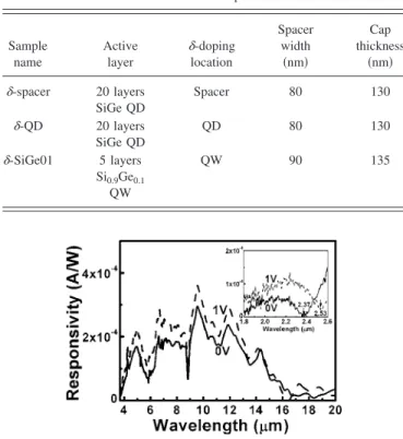
At 15 K, the absorption spectra can be grouped into three regions, including a 1.8– 2.37m peak 共the inset of Fig.2兲, a 3.7–6m peak, and a 6 – 16m peak共Fig.2兲. The
schematic energy levels in Si/ SiGe/ Si QDs are shown in Fig.3.
The 1.8– 2.37m peak results from the intervalence band transition 共E1 in Fig. 3兲 between heavy hole ground
state共HH1兲 and the continuum states. When the applied volt-age increases from 0 to 1 V, the cutoff wavelength shifts from 2.37m共0.52 eV兲 to 2.53m共0.49 eV兲 共the inset of Fig.2兲. Holes, which are excited by photons with energy less
than the energy difference between the ground state and the barrier, can tunnel through the triangular barrier at 1 V共Fig.
3兲. The redshift is characteristic of bound-to-continuum
transition.11,12
The photoluminescence共PL兲 spectrum at 10 K is shown in Fig. 4. Since the conduction band offset at the Si/ SiGe heterojunction is very small and the ground state 共HH1兲 is very close to the valence band edge of SiGe dots, the HH1-to-continuum transition energy approximately coincides with the energy gap difference between Si 共1.17 eV兲 and SiGe dots共0.7 eV兲.
The hole concentration of light hole ground state共LH1兲 is smaller than that of HH1. The LH1-to-continuum transi-tion should be much weaker than the HH1-to-continuum transition, and no obvious absorption is observed.
The 3.7– 6m peak results from the intersubband tran-sition 共E2 in Fig. 3兲 between the ground state of light hole 共LH1兲 and the first excited state of light hole 共LH2兲 in the SiGe-dot layers. The 3.7– 6m peak does not shift as the gate voltage increases, since the LH1-to-LH2 transition 共3.7–6m peak兲 occurs between two bound states, and the influence of a triangular barrier is small.
The continuous supply of holes to the SiGe/ Si QDs is necessary when the photogenerated holes are collected by the electrode at the bottom of the substrates 共Fig.5兲. Two
pos-sible mechanisms could be responpos-sible for the supply of holes. One is the electron-hole pair generation at oxide/ semiconductor interface. The electrons in the valence band jump into the conduction band via interface states, and tun-nel into the gate electrode through the thin oxide共2 nm兲, and
FIG. 1. The structure of the MOS SiGe/ Si QDIP. The 20-layer SiGe quan-tum dots were formed by ultrahigh vacuum chemical vapor deposition, and the␦doping was introduced in the Si spacer. The inset shows the TEM photograph of SiGe quantum dots.
TABLE I. Condition of three different samples.
Sample name Active layer ␦-doping location Spacer width 共nm兲 Cap thickness 共nm兲 ␦-spacer 20 layers SiGe QD Spacer 80 130 ␦-QD 20 layers SiGe QD QD 80 130 ␦-SiGe01 5 layers Si0.9Ge0.1 QW QW 90 135
FIG. 2. Spectral response of the␦-spacer sample at 0 and 1 V共15 K兲. The inset shows the response at shorter wavelength, indicating cutoff wavelength at 2.37m at 0 V and 2.53m at 1 V.
FIG. 3. The schematic energy levels in Si/ SiGe/ Si quantum dots under different biases. The band is not flat at 0 V since the flatband voltage is negative.
FIG. 4. The photoluminescence共PL兲 spectrum of the␦-spacer sample at 10 K. The band edge of the SiGe dot signal corresponding to HH1 to con-duction band in SiGe dot is⬃0.7 eV.
033117-2 Lin et al. J. Appl. Phys. 101, 033117共2007兲
the holes are left in the valence band. The other mechanism is that holes tunnel from the gate electrode to Si.
The 6 – 16m peak mainly comes from the intraband 共intersubband or intervalence band兲 transition in the boron
␦-doping wells in the Si spacers. For the shorter wavelength part in the 6 – 16m peak共about 6–10m兲, there are other possible transitions in QDs such as the intersubband transi-tion from HH1 to HH2 and the intervalence band transitransi-tion from HH1 to LH1. However, the excited states 共HH2 and LH1兲 are far from the top of the barrier, preventing photoex-cited carriers to be efficiently collected.13Therefore, the tran-sitions 共HH1 to HH2 and HH1 to LH1兲 may have a small contribution to the 6 – 10m absorption. Moreover, oxygen with an impurity level of 160 meV共7.8m兲 may also con-tribute to the 6 – 10m absorption.14
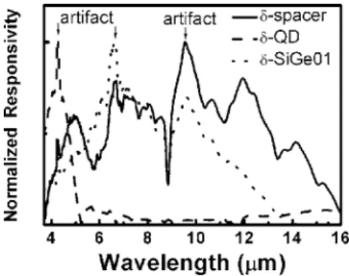
For comparison, the infrared spectra of the three samples in Table I are shown in Fig. 6. The cutoff wavelengths of
␦-spacer and␦-SiGe01 samples at the low energy end are 16 and 14m, respectively. These transitions result from the intraband transition of␦-doping well共Fig.7兲. The blueshift
of the cutoff wavelength of the ␦-SiGe01 sample as com-pared with the ␦-spacer sample is probably due to the addi-tional quantum confinement of Si0.9Ge0.1 QW outside the
␦-doping well. Note that there is a valence band offset of ⬃75 meV between Si and Si0.9Ge0.1. The long-wavelength 共⬍14m兲 transition in the ␦-SiGe01 sample cannot origi-nate from intraband transition of Si0.9Ge0.1 QW due to the
QW’s shallow depth, where the cutoff wavelength should be larger than 16.5m 共75 meV兲. No absorption around 6 – 16m is observed in the␦-QD sample. Since the valence band barrier of SiGe QD is large enough to block the photo-excited holes from the␦-doping well, the photoexcited car-riers cannot be collected by the electrode共Fig.7兲.
For the intersubband transition from LH1 to LH2, the cutoff wavelengths of the ␦-QD sample and the ␦-spacer sample are 5 and 6 m, respectively. The smaller cutoff wavelength of the ␦-QD sample may be due to the many body effect, since the hole concentration in the QDs is higher. The many body effect increases the intersubband transition energy.15,16
Note that there are some artifacts, such as 2.6, 4.3, 6.6, and 9.5m共Fig.6兲, due to the absorption from the
measure-ment environmeasure-ment.
The normalized detectivity D*is
D*=
冑
A⌬fNEP =
冑
A⌬fin/R , 共1兲
where A is the detector area 共3⫻10−2 cm2兲 and ⌬f is the equivalent bandwidth of the electronic system. The noise equivalent power is defined as in/ R, where in is the current noise and R is the responsivity. At 1 V, the current noise is limited by the dark current and can be approximated as the shot noise共2eId⌬f兲1/2, where I
dis the measured dark current. At 0 V, the dark current approaches zero, and the current noise should be approximated as Johnson noise共4kTG⌬f兲1/2, where G is the measured conductance.
Therefore, D* can be simplified as
D*=
冑
冑
AR2eId at 1 V, 共2兲
D*=
冑
冑
AR4kTG at 0 V. 共3兲
Figure8 shows the detectivity at 1 and 0 V bias at dif-ferent temperatures. At 15 K and 1 V bias, the peak detec-tivity is found to be 4.3⫻108cm Hz1/2/ W at 9.6m and 2.6⫻108cm Hz1/2/ W at 4.9m. The peak detectivity in-creases to 3.9⫻109cm Hz1/2/ W at 9.6m and 2.3 ⫻109cm Hz1/2/ W at 4.9m when the bias decreases from 1 to 0 V. Note that the conductance measured at 15 K is 2 ⫻10−7 S. The detectivity decreases as operating temperature increases. The values of detectivity are very low in
compari-FIG. 5. Two possible mechanisms responsible for the hole supply.共a兲 Elec-trons in the valence band jump into the conduction band via interface states and tunnel into the gate electrode through the thin oxide, and the holes are left in the valence band.共b兲 Holes tunnel from the gate electrode to Si.
FIG. 6. Comparison of the spectral responses of the␦-spacer sample, the
␦-QD sample, and the␦-SiGe01 sample at 15 K共at 1 V bias兲. Both the
␦-spacer sample and the ␦-SiGe01 sample have a long-wavelength transition.
FIG. 7. The schematic detection of long-wavelength infrared inside the
␦-doping layer. The long-wavelength infrared photoexcited carriers can be collected in the ␦-spacer sample and ␦-SiGe01 sample. No absorption around 6 – 16m is observed in the␦-QD sample, since the valence band barrier of SiGe QD is too large to block the photoexcited hole from the
␦-doping well.
033117-3 Lin et al. J. Appl. Phys. 101, 033117共2007兲
son with that of commercialized detectors. Further optimiza-tion should be done for higher detectivity. Dark current re-duction and responsivity enhancement may be the effective steps to improve the detectivity. The dark current could be reduced with a passivation technique to decrease the inter-face states at Si/LPD SiO2 interface. Antireflection coating could be used in order to increase the responsivity.
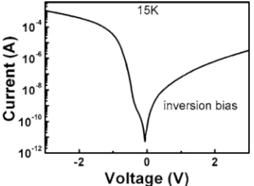
Under negative bias, the electrons in Al gate tunnel to the semiconductor, and this large dark current prevents the detector operation at the negative bias共Fig.9兲.
IV. CONCLUSIONS
There are three detection regions for the QDIP with␦ doping in the Si spacer, including 1.8–2.37, 3.7–6, and 6 – 16m. The 1.8– 2.37m peak results from the interval-ence band transition from HH1 to the continuum states in the SiGe-dot layers. The 3.7– 6m peak results from the
inter-subband transition from LH1 to LH2 in the SiGe-dot layers. The cutoff wavelengths of the LH1-to-LH2 transition of the
␦-QD and ␦-spacer samples are 5 and 6m, respectively. The blueshift of the ␦-QD sample may be due to the many body effect. The intraband transition in ␦-doping quantum wells contributes to long-wavelength infrared detection 共6–16m兲. The cutoff wavelengths at the low energy end of
␦-spacer and␦-SiGe01 samples are 16 and 14m, respec-tively. The blueshift of the cutoff wavelength of the
␦-SiGe01 sample is probably due to the additional quantum confinement of Si0.9Ge0.1QW outside the␦-doping well. At 15 K and 0 V, the peak detectivity is found to be 3.9 ⫻109cm Hz1/2/ W for the 6 – 16m peak and 2.3 ⫻109cm Hz1/2/ W for the 3.7– 6m peak.
ACKNOWLEDGMENTS
This work is supported by the U.S. Air Force Office of Scientific Research/AOARD under Contract No. FA 520904P0441 and the National Science Council, Taiwan, R.O.C. under Contract nos. 2221-E-002-357 and 95-2221-E-002-370.
1P. G. Datskos, S. Rajic, L. R. Senesac, and I. Datskou, Ultramicroscopy
86, 191共2001兲.
2J. Park, S.-J. Jo, S. Hong, and J.-I. Song, Solid-State Electron. 46, 651
共2002兲.
3G. Karunasiri, J. S. Park, J. Chen, R. Shih, J. F. Scheihing, and M. A.
Dodd, Appl. Phys. Lett. 67, 2600共1995兲.
4R. People, J. C. Bean, C. G. Bethea, S. K. Sputz, and L. J. Peticolas, Appl.
Phys. Lett. 61, 1122共1992兲.
5S. V. Bandara et al., Appl. Phys. Lett. 86, 151104共2005兲.
6J.-h. Zhu, D.-w. Gong, B. Zhang, F. Lu, C. Sheng, H.-h. Sun, and X.
Wang, Phys. Rev. B 54, 2662共1996兲.
7M. H. Liao, C.-H. Lin, C.-H. Lee, T.-H. Cheng, T.-H. Guo, and C. W. Liu,
ECS Meeting, Cancun, Mexico, No. 1278共2006兲.
8O. G. Schmidt and K. Eberl, Phys. Rev. B 61, 13721共2000兲.
9B.-C. Hsu, S. T. Chang, C.-R. Shie, C.-C. Lai, P. S. Chen, and C. W. Liu,
Tech. Dig. - Int. Electron Devices Meet. 2002, 91.
10C. W. Liu, M. H. Lee, C. F. Lin, I. C. Lin, W. T. Liu, and H. H. Lin, Tech.
Dig. - Int. Electron Devices Meet. 1999, 749.
11B. F. Levine, J. Appl. Phys. 74, R1共1993兲.
12V. D. Jovanovic, P. Harrison, Z. Ikonic, and D. Indjin, J. Appl. Phys. 96,
269共2004兲.
13R. P. G. Karunasiri, J. S. Park, Y. J. Mii, and K. L. Wang, Appl. Phys. Lett.
57, 2585共1990兲.
14S. M. Sze, Physics of Semiconductor Devices, 2nd ed.共Wiley, New York,
1985兲, Part 1, p. 21.
15G. Karunasiri, Jpn. J. Appl. Phys., Part 1 33, 2401共1994兲.
16Z. Chen, C. M. Hu, P. L. Liu, G. L. Shi, and S. C. Shen, J. Appl. Phys. 82,
3900共1997兲. FIG. 8. The detectivity of the␦-spacer sample at different temperatures. The
3.7– 6m detection has a peak at 4.9m, and the 6 – 16m detection has a peak at 9.6m.
FIG. 9. Dark current of the␦-spacer sample at 15 K. The detector is oper-ated at inversion bias.
033117-4 Lin et al. J. Appl. Phys. 101, 033117共2007兲