國 立 交 通 大 學
電子工程學系 電子研究所碩士班
碩 士 論 文
銦鎵摻雜之非晶態氧化鋅薄膜電晶體在環境與照光偏壓下穩定度
之研究
Study of Environment Effects and Bias Illumination Stability for
Amorphous Indium-Gallium-Zinc-Oxide Thin Film Transistors
研 究 生:李岳恆
指導教授:施敏
院士
指導教授:
張鼎張 博士
銦鎵摻雜之非晶態氧化鋅薄膜電晶體在環境與照光偏壓下穩定度之研究
Study of Environment Effects and Bias Illumination Stability for Amorphous
Indium-Gallium-Zinc-Oxide Thin Film Transistors
研 究 生:李岳恆 Student:Iue-Hen Li
指導教授:施敏 院士 Advisor:Prof. S. M. Sze
張鼎張 博士 Prof. Ting-Chang Chang
國 立 交 通 大 學
電子工程學系 電子研究所
碩 士 論 文
A Thesis
Submitted to Department of Electronics Engineering and Institute of Electronics
College of Electrical Engineering and Computer Science National Chiao Tung University
in partial Fulfillment of the Requirements for the Degree of
Master in
Electronics Engineering June 2011
Hsinchu, Taiwan, Republic of China
i
銦鎵摻雜之非晶態氧化鋅薄膜電晶體在環境與
照光偏壓下穩定度之研究
研 究 生:李岳恆 指導教授:施敏 院士
張鼎張 博士
國立交通大學電子工程學系電子研究所碩士班
摘要
近年來,隨著液晶顯示器的尺寸越來越大,用來使液晶旋轉的電晶體所需要 的電子遷移率(mobility)也必須越來越高,但是傳統的非晶矽薄膜電晶體的電子遷 移率太低(< 1 cm2 /V s) ,因此擁有高電子遷移率(<10 cm2/V s)的非晶金屬氧化物 薄膜電晶體對於未來顯示器的應用上非常有潛力,故銦鎵摻雜之非晶態氧化鋅 (α-InGaZnO)薄膜電晶體是我們所要研究的重點。 雖然α-IGZO薄膜電晶體有非高的電子遷移率,但往往會受到環境、照光以 及長時間操作偏壓而對元件產生起始電壓(threshold voltage)的偏移,故我們的實 驗分成兩大部分來探討,第一部分主要是針對α-IGZO薄膜電晶體對氣氛的關係, 我們可以發現到氧氣在含水的環境中或者是較高的溫度下可以更有效率的吸附 在α-IGZO薄膜電晶體上,造成起始電壓向右飄移。第二部主要為測試元件在照 光以及負偏壓下不穩定性的探討,在照長波常以及負偏壓的條件下可以看到電容 有一個提早抬升的趨勢,我們將這個現象歸因於有donor-like 型態的缺陷產生於ii
介面,但是這個現象在照短波長以及負偏壓下並看不到,這是因為照短波長的光 可以產生大量的電洞,這些電洞累積在介面,當在量測的時候這些累積的電洞屏 蔽掉了介面donor-like 型態的缺陷,導致在C-V的量測上沒有提早抬升的趨勢。
iii
Study of Environment Effects and Bias
Illumination Stability for Amorphous
Indium-Gallium-Zinc-Oxide Thin Film Transistors
Student:Iue-Hen Li
Advisor:Prof. S. M. Sze
Prof.
Ting-Chang Chang
Department of Electronics Engineering and Institute of Electronics
National Chiao Tung University
Abstract
In recent years, the higher mobility is needed for thin film transistor (TFT) mainly used to twist the liquid crystal for the larger size display. The mobility of traditional amorphous silicon TFT is too low (< 1 cm2/V s), while the amorphous metal oxide has mobility higher than 10 cm2/V s, which is a very promising material for the future display application. Therefore, the amorphous Indium-Gallium-Zinc-Oxide (α-InGaZnO) is the main topic that we want to research.
Although the α-IGZO TFT has very high mobility, it is always suffer from the instability of environment, illumination and long term bias stress which cause the threshold voltage (VTH) shift. We can separate our study into two parts. The first part
we want to discuss is the relation between the α-IGZO TFT and oxygen. We found that oxygen absorbs on α-IGZO is much more efficiently under water-containing or
iv
higher temperature condition, causing a positive threshold voltage shift. The second part is mainly the examination of α-IGZO TFT instability under the negative bias stress with light. We can find that the stretch-out phenomenon of C-V transfer curve under negative bias stress with long wavelength of light. We contribute this phenomenon to the donor-like traps creation at the interface between gate insulator and channel. However, the C-V transfer curve stretch-out phenomenon disappeared under the negative bias stress with short wavelength of light. It may be due to the huge amount of holes generated through illumination with short wavelength of light. These holes could accumulate at the interface and screen the donor-like traps.
v
Acknowledgement
碩士生活兩年很快就過去了,這兩年來,一路從新竹修課到高雄做實驗,讓 我得到的不僅只是知識上的充實,也讓我體會到很多待人處事的道理,我十分感 謝施敏老師以及張鼎張老師,總是不厭其煩的在 group meeting 中教導相關的知 識,使我在半導體相關的領域可以懂得更多,看得更廣,以及在我研究上的指導 與論文的修改,使得當我在困難以及不知所措時可以得到解決。 另外我特別想感謝的是宛芳學姊,很感謝學姊不厭其煩地教導我有關研究領 域相關的知識、機台的量測、數據分析等等…,在我做實驗的時候往往能夠得到 學姊的幫忙,使得研究不會像無頭蒼蠅般的亂做一通,另外我要感謝富彥、美娜、 書瑋、原瑞、柏鈞、敏甄、佳盛、志豪、仕承、德智、詠恩、冠張、禹鈞、侑廷、 聖堯、學志、文宏、侑廷、耿維、君寶、天宇等學長姐於研究過程中給予建議及 指正,感謝一起走過這段日子的同學們:柔妙、菀琳、儀憲、凱弘、雅琪、承瑋、 國孝、偉立、奕介、祐松、冠任、志誠等,總是可以在我實驗碰到瓶頸的時候陪 我聊天散心以及加油打氣,以及碩一的學弟妹們:昌蓓、哲丘、君昱、明諺、峻 豪、天健等,有你們,讓實驗室變得好熱鬧,看你們在實驗室專心的準備期中期 末考,似乎又讓我回到了碩一的時光,還有要感謝遠在新竹的Q博,在我在高雄 做實驗的期間,總是很辛苦地幫我打點好學校一些大大小小的事情,讓我不用來 回奔波,以及在SD中的文少與vivian,讓我在閒暇時刻不會感到無聊。 最後我想感謝的是我的家人:把我照顧得很好的爸爸、三不五時從紐西蘭打 網路電話回來關心我的媽媽、幫我修改英文的哥哥與常常帶我去看電影以及吃早 午餐的阿姨,有你們的關心與照顧,使得我在做研究的時候沒有後顧之憂,讓我 得以重整思緒重新出發。因為有你們,得以讓我完成此本碩論,Thank you all。李岳恆 謹識 交通大學 2011 年
vi
Contents
Chinese Abstract ... i
English Abstract ... iii
Acknowledgement ... v
Contents ... vi
Figure Captions ... viii
Chapter 1 Introduction ... 1
1.1 Amorphous Oxide Semiconductor ... 1
1.2 Origin of High Electron Mobility for Amorphous Oxides Semiconductor ... 2
1.3 The Promising Material of Amorphous Oxide Semiconductor ... 3
1.4 Why Use a-IGZO? ... 4
Chapter 2 Motivation ... 10
2.1 Illumination instability ... 10
2.2 Electrical Instability... 14
2.3 Environment Instability ... 19
Chapter 3 Fabrication and Characterization ... 25
3.1 Fabrication Process of a-IGZO TFTs ... 25
3.2 Methods of Device Parameter Extraction ... 26
Chapter 4 Results & Discussion ... 28
4.1 Water Induce Oxygen Adsorption ... 28
4.2 Oxygen Adsorption Would Passivate Trap ... 33
4.3 Negative Illumination Bias Stress Instability (NBIS) ... 52
vii
5.1 Oxygen Absorption Effect ... 70
5.2 Negative Illumination Bias Stress Effect ... 70
Reference ... 71
viii
Figure Captions
Chapter 1
Introduction
Figure 1-2-1 Band gap formation mechanisms in (a) covalent and (b,c) ionic semiconductors.
[1.1]
………..7
Figure 1-2-2 Schematic orbital drawings for the carrier transport paths (conduction band bottoms) in crystalline and amorphous semiconductors.
………...………..7
Figure 1-3-1 Graphical summary of require carrier mobility for future displays.[1.3]
………...………...………..8
Figure 1-4-1 Amorphous formation of IGZO thin films.[1.1]
………9
Figure 1-4-2 Electron transport properties of IGZO thin films.[1.1]
…...…9
Chapter2
Motivation
Figure 2-1-1 Qualitative description of UV-illumination effects.[2.2]
..…...13
Figure 2-1-2 A possible atomicconfiguration model for metastable donor model.The large red sphere shows a weakly bonded oxygen ion, and the lightred sphere shows a metastable site.[2.3]
………...13
Figure 2-2-1 Comparison of the effect of a positive and a negative gate biasstress on the transfer characteristics. [2.18]
………...17
Figure 2-2-2 Hysteresis sweeps −10 to 10, −20 to 20, and −30 to 30 V weremade consecutively. [2.18]
……...17
Figure 2-2-3 Subgap DOSs extracted from the device simulations. [2.21]...18
Figure 2.3.1 The Schematic diagram of oxygen molecular adsorbed on theix
Figure 2.3.2 The electron in the conduction band are cpatured by oxygen, the space charge are appaer causing an upward band bending.
………....22
Figure 2.3.3 The Schematic diagram of water molecular donor elecrons toα-IGZO TFT. [2.29]
………...…....23
Figure 2.3.4 The Schematic band diagram of water been as trap for (a) thinner(b) thicker.
…...………...23
Figure 2-3-5 Schematic showing the electric-field-induced (a) adsorption ofoxygen molecules and (b) desorption of water molecules under positive gate bias stress. [2.28]
…...24
Chapter3
Fabrication and Characterization
Figure 3-1-1 The device structure of α-IGZO TFT………25
Chapter 4
Result & Discuss
Figure 4-1-1 The measurement system for different ambient condition……...30
Figure 4-1-2 The I-V transfer curve under different partial pressure of
nitrogen……….……30
Figure 4-1-3 The I-V transfer curve under different partial pressure of
oxygen...31
Figure 4-1-4 The I-V transfer curve under different partial pressure of water-containing oxygen. ...31
Figure 4-1-5 The threshold voltage shift for different ambient. ...32
x
Figure 4-2-2 The I-V transfer curve for different partial pressure of the oxygen molecular which absorbed on α-IGZO at 273K………40
Figure 4-2-3 The I-V transfer curve for different partial pressure of the oxygen molecular which absorbed on α-IGZO at 303K………41
Figure 4-2-4 The I-V transfer curve for different partial pressure of the oxygen molecular which absorbed on α-IGZO at 333K. …………..…41
Figure 4-2-5 The I-V transfer curve for different partial pressure of the oxygen molecular which absorbed on α-IGZO at 363K. ……..………42
Figure 4-2-6 The threshold voltage (VTH) shift under different oxygen partial
pressure at different temperature. ..……….….42
Figure 4-2-7 The subthreshold swing (S.S.) shift under different oxygen partial pressure at different temperature……….….43
Figure 4-2-8 The C-V transfer curve of α-IGZO TFT. ……….43
Figure 4-2-9 The surface potential as a function of gate voltage. ………..…..44
Figure 4-2-10 (a) The flat band condition (b) The maximum surface potential as gate voltage larger than threshold voltage (VTH) of α-IGZO. 44
Figure 4-2-11 The maximum surface potential as a gate voltage larger than threshold voltage. ………..…..45
Figure 4-2-12 The density of state of of α-IGZO TFT. ………..45
Figure 4-2-13 The C-V detects range among two red dash lines. [4.8] …...…..46
Figure 4-2-14 The C-V transfer curve for different partial pressure of the oxygen molecular which absorbed on α-IGZO at 273K. ………..46
Figure 4-2-15 The C-V transfer curve for different partial pressure of the oxygen molecular which absorbed on α-IGZO at 303K. ………..……47
Figure 4-2-16 The C-V transfer curve for different partial pressure of the oxygen molecular which absorbed on α-IGZO at 333K. ..………47
xi
Figure 4-2-17 The C-V transfer curve for different partial pressure of the oxygen molecular which absorbed on α-IGZO at 363K………....48
Figure 4-2-18 The density of state for different partial pressure of the oxygen molecular which absorbed on α-IGZO at 273K. …………...48
Figure 4-2-19 The density of state for different partial pressure of the oxygen molecular which absorbed on α-IGZO at 303K. ………..49
Figure 4-2-20 The density of state for different partial pressure of the oxygen molecular which absorbed on α-IGZO at 333K. ………...……..49
Figure 4-2-21 The density of state for different partial pressure of the oxygen molecular which absorbed on α-IGZO at 363K. …...……..50
Figure 4-2-22 The flat band voltage shift for back to back sweep under vacuum and vacuum which is oxygen already absorbed. ...……..50
Figure 4-2-23 The schematic band diagram of flat band voltage (VFB) shift
because of charge trapping in the a-IGZO. ...………..…..51
Figure 4-3-1 The I-V transfer curve under 653 nm wavelength of light illumination. ………..…..60
Figure 4-3-2 The C-V transfer curve under 653 nm wavelength of light illumination. ………..…..60
Figure 4-3-3 The I-V transfer curve under 556 nm wavelength of light illumination. ………..…..61
Figure 4-3-4 The C-V transfer curve under 556 nm wavelength of light illumination. ………..…..61
Figure 4-3-5 The I-V transfer curve under 500 nm wavelength of light illumination. ………..…..62
Figure 4-3-6 The I-V transfer curve under 500 nm wavelength of light illumination. ………..…..62
xii
Figure 4-3-7 The subgap density of state distribution forα-IGZO. [4.8]…….63
Figure 4-3-8 The schematic of electron in the deep trap under three different wavelength illumination condition. ……….63
Figure 4-3-9 The I-V transfer curve under 653 nm wavelength of light illumination and VG-VTH = -30V. ………...…….64
Figure 4-3-10 The C-V transfer curve under 653 nm wavelength of light illumination and VG-VTH = -30V. ………...…….64
Figure 4-3-11 The I-V transfer curve under 556 nm wavelength of light illumination and VG-VTH = -30V. ………...…….65
Figure 4-3-12 The C-V transfer curve under 556 nm wavelength of light illumination and VG-VTH = -30V. ………...…….65
Figure 4-3-13 The I-V transfer curve under 500 nm wavelength of light illumination and VG-VTH = -30V. ………...…….66
Figure 4-3-14 The IC-V transfer curve under 500 nm wavelength of light illumination and VG-VTH = -30V. ………...…….66
Figure 4-3-15 The ISE-TCAD C-V simulation for α-Si TFT with donor-like state below Ei. ………..…...…….67
Figure 4-3-16 (a)The schematic of donor-like trap generate region within the bandgap of a-IGZO under NBIS. (b) Only the donor-like trap near source and drain could contribute to C-V transfer curve stretch-out. ……….………..…...…….67
Figure 4-3-17 The schematic is (a) hole could generate donor-like interface trap (b) too much holes accumulate at the interface. ……..…...…….68
Figure 4-3-18 (a) the donor-like trap could become neutral as below Fermi level. (b) the donor-like trap could not become neutral as below Fermi level because the accumulated holes screen it………68
xiii
Figure 4-3-19 The C-V stretch-out appears in the recovery under dark environment………..69
Figure 4-3-20 The C-V stretch-out appears in the recovery under dark environment after negative gate bias stress with 653nm wavelength of light. ………...………..69
Figure 4-3-21 The schematic of α-IGZO band diagrame with donor-like defects (a) without hole trapping (b) with hole trapping, which measure from neagetive gate bias. ………..70
1
Chapter 1 Introduction
1.1 Amorphous Oxide Semiconductor
Amorphous semiconductors have created a new area of electronics devices such as solar cells and active-matrix (AM) flat-panel displays. Single-crystalline semiconductor technology, typified by crystal silicon electronics, is unsuitable for such applications, whereas amorphous or polycrystalline films can be easily formed.
Due to carrier scattering and trapping at grain boundaries in polycrystalline materials (the grain boundary problem), hydrogenated amorphous silicon (α-Si:H) has been used more widely than polycrystalline silicon (p-Si) for practical large-size applications. However, the critical obstacles to be overcome for α-Si:H in future applications is low mobility (< 1 cm2/Vs) and instability against electric stress and photo-illumination.
Amorphous oxide semiconductor (AOS) materials have superior characteristics to conventional semiconductors, and therefore AOS TFT technology has grown very rapidly toward the realization of TFT backplanes for next-generation flat-panel displays. AOS TFTs have several features that are attractive for flat-panel displays and large-area integrated circuits. The advantageous features of AOS TFTs are summarized as follows:
Low processing temperature: AOS TFTs exhibit satisfactory operation
characteristics even if fabricated at room temperature.
High electron mobility: AOSs exhibit high Hall and TFT mobility of
> 10 cm2/V s by choosing appropriate chemical compositions.
2
chemical bonds, and therefore they form much fewer defect states in the band gap than conventional covalent semiconductors such as silicon. The low defect density allows small subthreshold swing and low operation voltages.
Large allowance in the choice of gate insulator: a variety of gate insulators
have been examined for AOS TFTs, and good operation characteristics have been demonstrated. This feature would also benefit for two reasons: the unipolarity of AOS, by which only electrons are mobile and thus the valence band offset between the gate insulator and AOS is not critical; and the high ionic chemical bonding nature, which gives rise to fewer defects at the gate insulator/AOS interfaces.
Simple electrode structure and low off current: Silicon-based field-effect
transistors require a p–n junction for the source and drain electrodes to suppress inversion operation and the consequent increase in off current. Since AOS TFTs have not exhibited inversion p-channel operation, simple metallic contacts may be used for source and drain electrodes without increasing the off current.
[1.1]
1.2 Origin of High Electron Mobility for Amorphous Oxides
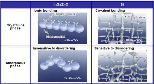
Semiconductor
It is believed that the properties of amorphous semiconductors are considerably degraded compared with their corresponding crystalline phases, which is actually the case for silicon because intrinsic crystalline silicon (c-Si) exhibits an electron mobility of 1500 cm2/V s, which deteriorates to less than 2 cm2/V s in α-Si:H. On the other hand, AOSs exhibit large electron mobilities of greater than 10 cm2/V s even in amorphous structures. It benefits from the strong ionicity of oxides. In silicon, the conduction band minimum (CBM) and valence band maximum (VBM) are made of
3
anti-bonding (sp3 σ*) and bonding (sp3 σ) states of Si sp3 hybridized orbitals, and its band gap is formed by the energy splitting of the σ*–σ levels as shown in Figure 1-2-1(a). By contrast, oxides have strong ionicity and charge transfer occurs from metal to oxygen atoms as shown in Figure 1-2-1(b), and the electronic structure is stabilized by the Madelung potential formed by these ions, raising the electronic levels in cations and lowering the levels in anions. Consequently, the CBM is primarily formed by the unoccupied s orbitals and the VBM of cations by fully occupied O 2p orbitals, as illustrated in Figure 1-2-1(c).
Conventional amorphous semiconductors such as α -Si:H exhibit much deteriorated carrier transport properties compared with the corresponding crystalline materials. This is because the chemical bonds in the covalent semiconductors are made of sp3 or p orbitals with strong spatial directivity. By contrast, the CBMs of non-transition metal oxides are made of the spherically extended s orbitals of metal cations, and their overlaps with neighboring metal s orbitals are not altered appreciably by the disordered amorphous structure; therefore, the electronic levels of the CBM are insensitive to local structural randomness, and electron transport is not affected significantly as shown in Figure 1-2-2.
1.3 The Promising Material of Amorphous Oxide Semiconductor
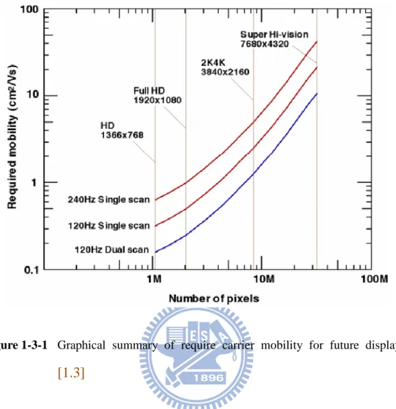
As the size and the resolution of digital television (TV) increase, switching devices with higher electron mobility are required because the charging time for each pixel decreases in addition to the increased RC delay in the signal lines. It is estimated that electron mobility over 3 cm2 / V s is required for driving the ultrahigh-definition(7680 × 4320) TV at 120-Hz frame rate. The required mobility will be even higher for displays with higher resolution, a faster frame rate and a larger
4
panel size as shown in Figure 1-3-1. Recently, three-dimensional (3D) displays have appeared on the market with panel sizes of ∼55 inches and frame rates of 240 Hz. However, higher frame rates of 480 Hz are required to improve the picture quality because a 3D display must project two or more picture frames alternately for the left and right eyes.
On the other hand, there are other applications of TFTs, such as “system-on-glass” and “system-on-panel” technologies, which are used in the mass-produced, small-size flat-panel displays in mobile phones. The circuits are currently constructed from poly-Si TFTs because these applications require high TFT mobility for high-speed driver/peripheral circuits, and complementary metal-oxide semiconductor logic circuits are used to achieve ultra-low power consumption. It has also been reported that amorphous amorphous Indium-Gallium-Zinc-Oxide (α-IGZO) can be used as resistance random access memory (ReRAM).
[1.2]
AOS TFTs are also expected to be developed for memory, pixel driver and other peripheral circuits in the same flat panel once a larger Hall mobility of AOS exceeds 50 cm2/V s and other suitable property are realized.[1.1, 1.3]
1.4 Why Use α-IGZO?
The most essential feature of a semiconductor is that the carrier concentration should be controllable over several orders of magnitude. Oxide TFTs have been fabricated using ZnO, but the material known as a good transparent conducting oxide, contains a high density of mobile electrons (typically >> 1018 cm-3) even in nominally undoped states. This causes a serious problem for TFTs by making it difficult to control the channel conductance and the threshold voltage. This feature often results in instability of TFT characteristics.
5
The pure ZnO and In2O3 form crystalline films even when deposited at room
temperature. This is widely observed for many metals and oxides, for which it is difficult to obtain amorphous phases as shown inFigure 1-4-1. On the other hand, the binary oxide compounds, such as Zn-In-O and Zn-Ga-O, form amorphous phases if the mixing ratio of the oxides exceeds a certain threshold value. In general, mixing of two or more cations having different ionic charges and sizes is effective for enhancing the formation of an amorphous phase and suppressing crystallization; this is the reason why AOSs are basically multi-component systems, and this fact implies that we can find a rich variety of AOS materials.
Indium, gallium, zinc and tin are the major consistents of good transparent conducting oxides, and their unoccupied s orbitals form the electron transport paths in AOSs; therefore, having a majority of these ions is the fundamental requirement to obtain AOSs with large electron mobilities. To understand the role of the other ions, it is useful to compare systems such as α-IZO and α-IGZO. As seen in Figure 1-4-2, a-IZO has higher electron mobilities than α-IGZO, but is much more difficult to control at the low electron concentrations required for TFTs. Ga-O bonds are much stronger than In-O and Zn-O bonds, meaning that the incorporation of gallium suppresses the formation of oxygen deficiencies and the consequent generation of mobile electrons. On the other hand, the incorporation of high gallium content deteriorates the electron mobility. Therefore, the addition of an appropriate amount of a stabilizer ion that forms a strong chemical bond with the oxygen ion is important to obtain stable AOS materials and TFTs.
[1.1], [1.3]
Although there are many pros for α-IGZO, it still needs to solute some other issue for α-IGZO. The instability of metal oxide TFTs remains as an obstacle to overcome for practical applications to electronic devices. The device stability is
6
sensitive to bias/current stress, temperature, light illumination, and water vapor exposure.
The unit pixel circuit of an active matrix organic light-emitting diode (AM-OLED) is basically comprised of two transistors, the switching and driving transistors. The current flowing through the OLED is controlled by a drive thin-film transistor (TFT). During the programming cycle, the gate of the drive TFT is charged to a programming voltage through a switch TFT to control the luminance of the pixel during the rest of the frame time. In the case of the switching transistor, the variation of the mobility and threshold voltage is less important. However, the brightness of each pixel is highly dependent on the drain current of the driving transistor. For example, a threshold voltage (VTH) shift of the driving transistor causes a change in
the resulting luminance of OLED diodes. Thus, the VTH shift in α-IGZO which is
7
Figure 1-2-1 Band gap formation mechanisms in (a) covalent and (b,c) ionic
semiconductors.
[1.1]
Figure 1-2-2 Schematic orbital drawings for the carrier transport paths (conduction
8
Figure 1-3-1 Graphical summary of require carrier mobility for future displays.
9
Figure 1-4-1 Amorphous formation of IGZO thin films.
[1.1]
10
Chapter 2 Motivation
2.1 Illumination instability
α-IGZO TFT is usually used as driving the current which is through the AM-OLED. However, for such device in the flat panel is almost always exposed to back light. This would cause a negative threshold voltage (VTH) shift of α-IGZO TFT
to affect the brightness of AM-OLED. Hence, the instability of illumination is the quit important issue to consider.
There are several models to explain the instability of illumination. Most general thinking is that the α-IGZO suffer from the light illumination would generate electron-hole pair. Because the energy band gap of α-IGZO is about 3.0eV [2.1] and the wavelength for visible light is about 400~700 nm (energy is about 1.77~3.1eV), once the energy of light larger than the bandgap of α-IGZO, the electrons in the valence band would have chance to excite to conduction band and contribute to the free electrons. This will lead to the increase in conductivity and the decrease in threshold voltage (VTH).
Takechi et al [2.2] attribute the instability to the structure change during the illumination and the possible explanation for the structure change is the generation of oxygen vacancies, which provide free electrons and interstitial oxygen atoms as show in Figure 2-1-1. The significant threshold voltage (VTH) decrease is owing to those
free electrons generated mainly by this way. Moreover, when switching off the light, it could find that slow recovery of threshold voltage (VTH). It results from the
reversible structure change which involves the recombination of oxygen vacancies, free electrons and oxygen atoms. Through illumination, it offers sufficient energy for oxygen atom to diffuse into an interstitial site. However, after switching off light, the
11
interstitial oxygen atoms require relatively high energies to diffuse back to original site.
Lee et al [2.3] – [2.4] also indicate that the illumination of α-IGZO would cause the metastable donor state with long decay time. Due to α-IGZO contains the weakly bounded oxygen ions with small formation energy of an oxygen deficiency as shown in Figure 2-1-2. Ghaffarzadeh et al [2.5]show that the recovery time is dependent on the temperature when switching off light. With the higher temperature the shorter recovery time is needed which means the drain current decay rapidly due to the quick negative threshold voltage (VTH) shift as the time getting longer at higher temperature.
It implies that structure relaxes or the metastable donor state vanishes sooner.
Another report [2.6] – [2.8] thought the decrease in threshold voltage (VTH) is
due to the neutral oxygen vacancy (VO) of original α-IGZO which creates a defect
localized state in the band gap and doses not contribute to the conduction band. Under illumination, light could cause photoionization of neutral oxygen vacancies ( or ). The and states have higher energy level in the bandgap so electrons could contribute to the conduction band, hence led to the decrease in threshold voltage (VTH). Besides, the slow recovery of threshold
voltage (VTH) is thought to be that it should take several minute that the ionization
oxygen vacancy 、 ) can decay to zero.
Park [2,9] thinks that the oxygen vacancy (VO) generated by UV light before
negative bias stress operation would act as hole trap center in the bulk or at the semiconductor/gate insulator interface. These trap center could trap hole to become charged (VO+2) when operating in the negative bias stress and diffuse toward the
semiconductor/gate insulator boundary. This would provide positive charge buildup consequently and cause more severe negative threshold voltage (VTH) shift than the
12
Although these are so many models to explain the illumination instability of α-IGZO TFT, there is still no clear way to solve this natural problem.
13
Figure 2-1-1 Qualitative description of UV-illumination effects.[2.2]
Figure 2-1-2 A possible atomicconfiguration model for metastable donor model.
The large red sphere shows a weakly bonded oxygen ion, and the lightred sphere shows a metastable site.[2.3]
14
2.2 Electrical Instability
The electrical instability for α-IGZO TFT is a main issue in the application of flat-panel displays (FPDs). It is commonly used as switching TFT or drive TFT on FPDs for active-matrix liquid crystal displays (AM-LCDs) or organic light emitting diodes (AM-OLED). If the instability occurs in the switching TFT, that will affect the twist of liquid crystal and cause the problem of color rendering. On the other hand, if the instability occurs in the drive TFT, the current flow through the AM-OLED device will change. That would lead to variations in the respective pixel brightness. So the bias stress test for long-term reliability is an important factor in the TFT application.
Several reports has shown the electrical instability for α-Si [2.10] – [2.14], ploy-Si [2.15] and amorphous oxide semiconductor [2.16] – [2.17] as active layer. The reason to explain instabilities for α-IGZO TFT is the carrier trapping. Suresh
[2.18] showed that the I-V transfer characteristic of α-IGZO TFT, Figure 2-2-1, under a positive bias stress could cause a positive threshold voltage shift. This phenomenon results from electrons being trapped at the channel/dielectric interface or injected into the gate dielectric which screen the applied gate voltage, thus a larger positive gate voltage is required for the device to turn on, causing positive threshold voltage (VTH)
shift. The electrons trapping model could also explain the hysteresis loop for the C-V back-to-back measurement (VG =−10 to 10, −20 to 20, and −30 to 30 V) which shows in Fig 2-2-2. It indicates the successively flat band voltage (VFB) shift due to
higher positive voltage for each hysteresis loop in the return sweep.
On the other hand, unlike α-Si TFT [2.12], the threshold voltage of α-IGZO TFT under negative bias stress or the flat band voltage of forward C-V sweep is essentially no change. This means no positive charges (holes) can be trap at the channel/dielectric interface or get injected into the gate dielectric rather than positive charge cannot trap
15
at the channel/dielectric interface or get injected into the gate dielectric. There are two reasons explain why no hole in α-IGZO. Nomura et al [2.19] found that high-density electron traps in the subgap ( >1020 cm-3) where exist above valence band maximum with the energy range of ~1.5 eV which is detected hard X-ray photoemission spectroscopy (HX-PES). Hence the Fermi level (EF) will pin at this energy level
because the high-density electron traps are more than two orders of magnitude greater than a hole density (~1018 cm-3) induced by a gate voltage in a typical TFT structure, i.e. those huge amount of electrons in the high-density traps cannot be remove by negative bias. On the other hand, in spite of the high-density electron traps could be remove completely, hole is localized due to the disordered atomic configuration in α-IGZO break the coherent hybridization of O 2p orbitals which mainly form valence band [2.1].
The better describe the time evolution of threshold voltage which caused by the carrier trap at the channel/dielectric interface or get injected into the gate dielectric is the stretched-exponential model [2.13].
{ [ ( ) ]} (2.2.1)
(2.2.2)
(
) (2.2.3)
In the above equations, the is the effective voltage drop across the gate insulator (or also called effective stress voltage); is the initial threshold voltage; is the stress voltage which is applied by gate; represents the characteristic trapping time of carriers where the thermal activation energy is given by , with being the stretched-exponential exponent; is the average effective energy barrier that carriers in the channel need to overcome before they can enter the insulator, with being the thermal prefactor for emission over the barrier.
16
Fitting threshold voltage shift with stress time from equation (2.2.1) could get and , extract by applying equation (2.2.3) to the versus plots. The is extracted from α-IGZO TFT by Fung. [2.20] for positive bias temperature stress (0.78 eV) is smaller than the value of negative bias temperature stress (2.16 eV). Fung. suggests that the electrons are experienced a lower energy barrier than holes do during the charge injection process near the channel/dielectric interface. However, (1) the electron transport in the conduction band is composed of s orbital which is different from the hole that transport in the valence band which is sp3 hybridized orbital. Carrier migration under amorphous condition in the s orbital is more easily than sp3 hybridized orbital due to the orientation. (2) According to previous study [2.4], the conduction band offset is usually larger than valence band offset. So the means not only the carrier experienced energy barrier near the channel/dielectric interface but also the barrier which is carrier transport in orbital. Gelatos [2.12] extracted the for positive bias stress is 0.98 eV and for negative stress is 1.03 eV form α-Si:H TFT. The energy barrier for both electrons and holes needed to overcome to trap are quit equal. Hence the main dominant for carrier trapping mechanism seems the energy barrier which is carrier transport rather than the energy barrier of band offset.
Another possible mechanism for electrical instability is the shallow trap creation
[2.21] (the subgap density of states in the energy region close to conduction band) under constant current stress by simulation method which showed in Figure 2-2-3. The formation of the extra shallow traps is considered to be related to the breaking of the weak chemical bonds and subsequent formation of defects such as vacancy defects and low valence state cations.
17
Figure 2-2-1 Comparison of the effect of a positive and a negative gate bias stress
on the transfer characteristics. [2.18]
Figure 2-2-2 Hysteresis sweeps −10 to 10, −20 to 20, and −30 to 30 V were made
18
19
2.3 Environment Instability
Bottom-gate structured is common used for TFT because this kind of structure is easily formed owing to the deposition of channel layer and single mask step to form the source and drain electrodes. Several reports [2.22] – [2.26]showed the ZnO-based material is very sensitive to environment condition. The α-IGZO is one of the ZnO-based material, once the back-channel surface is exposed to the atmosphere, the α-IGZO TFT characteristics can be affect by the adsorption, desorption and diffusion of atmospheric gases causing instability.
The major gases in the air which affect the α-IGZO TFT instability are oxygen. Some reports [2.27] – [2.28] indicated the oxygen α-IGZO could be absorbed on the α-IGZO TFT channel as shown in Figure 2.3.1 and lead to threshold voltage increase. The reason is that oxygen capture an electron form the conduction band of α-IGZO and the resulting oxygen species can exist in O2-. At the same time, because the
electron is captured by oxygen form the α-IGZO, the depletion region formed owing to the charge transfer and the positive space charge which appear in the α-IGZO bulk, this would cause an upward band bending as shown in Figure 2-3-2. In such condition just like applied a negative bias in the back channel, so the larger threshold is needed to turn on the α-IGZO TFT (like MOSFET body effect).
(2.3.1) The oxygen capture an electron form the α-IGZO TFT channel can be described by the equation the equation (2.3.1). The equilibrium constant K is given by [ ] [ ] , where [ ] , , and [ ] are the adsorbed oxygen concentration on the α-IGZO surface, the partial oxygen pressure, and the electron density in the channel, respectively. As increase in , the concentration of [ ] increase because the equilibrium constant K should be invariant at a fixed
20
temperature. Likewise, when gate is applied positive voltage, the accumulated electron density [ ] in the channel region increase and the concentration of the adsorption [ ] is also increase. Both results in a positive threshold voltage shift.
On the other hand, much research for the effect of water (H2O) adsorption on the
α-IGZO TFT has been studied. Park et al [2.29] reported that H2O can act as electron
donor as shown in Figure 2-3-3 as well as acceptorlike trap when the water absorbed on the α-IGZO TFT channel. Once H2O donates a negative charge to the α-IGZO,
forming a back channel layer with a high electron concentration, could lead to a more negative threshold voltage shift. Also, water could also form acceptorlike trap in the α-IGZO TFT bulk. This effect is proved by the different bulk thickness of α-IGZO TFT sample because the water molecular could diffuse into the α-IGZO. For thicker α-IGZO, the water molecular cannot diffuse into too deep region of α-IGZO film. Although many acceptorlike traps are created, the created traps neither respond to the applied gate voltage as a trapping center, nor contribute to the gate swing change because the Fermi level near the back channel region is pinned when the gate voltage is applied. This also cause the electron could not be trapped in the acceptorlike defect. On the other hand, for the thinner α-IGZO films, the degradation of the subthreshold swing was enhanced due to the created trap could full response to the applied gate voltage as shown in Figure 2.3.4.
Furthermore, oxygen and water are not only naturally absorbed/desorption by physical or chemical bonding but also related to the electrical field. Jeong et al [2.28]
indicated that the oxygen and water could adsorbed/desorbed on the surface of the α-IGZO film under the influence of an electric field electrical. The electric field induced adsorption of oxygen molecules from the ambient atmosphere under the application of positive gate voltage stress as shown in Figure 2.3.4 (a). However,
21
under the positive gate bias stress could lead to the water molecules desorption form the α-IGZO film. It is an opposite trend to oxygen as shown in Figure 2.3.4 (b).
Recently, the zinc–tin oxide (ZTO) TFT which is also one of the ZnO-based materials showed negative threshold voltage (VTH) shift when exposed to various
organic solvents. Such result can be explained by terms of polarity or electronegativity of the adsorbed solvent molecules. When solvent molecules are adsorbed on the back channel surface, extra electron carriers can be accumulated near the channel surface possibly due to electronegativity of the solvent molecules. If the adsorbed solvent molecule has higher polarity (higher dielectric constant) and thus higher electronegativity, then the number of accumulated carriers near the surface will be larger compared to solvent molecule with lower polarity. It is possibly due to more downward band bending near the back channel surface thus higher negative threshold voltage (VTH) shift caused by adsorption of high-polar solvent molecules [2.30]. Base
on the same reason, α-IGZO TFT may suffer such the same result under the same condition, the back channel effect which exposure to atmosphere is an essential problem.
In order to solve the α-IGZO TFT instability problem, it is usually deposition another passivation layer such as SiO2 [2.31], SiNX[2.32], Al2O3 [2.33], TiOX[2.34]
22
Figure 2.3.1 The Schematic diagram of oxygen molecular adsorbed on the α-IGZO
TFT.
Figure 2.3.2 The electron in the conduction band are cpatured by oxygen, the space
23
Figure 2.3.3 The Schematic diagram of water molecular donor elecrons to α-IGZO
TFT. [2.29]
Figure 2.3.4 The Schematic band diagram of water been as trap for (a) thinner (b)
24
Figure 2-3-5 Schematic showing the electric-field-induced (a) adsorption of oxygen
molecules and (b) desorption of water molecules under positive gate bias stress. [2.28]
25
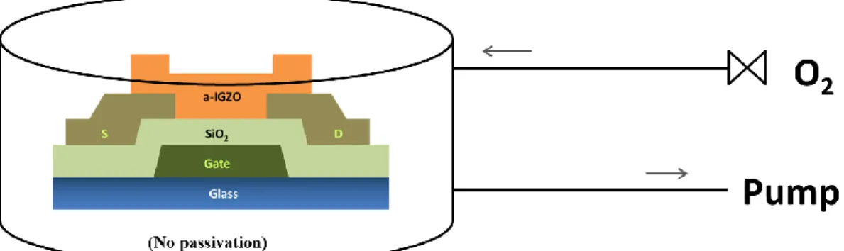
Chapter 3 Fabrication and Characterization
3.1 Fabrication Process of α-IGZO TFTs
Bottom gate coplanar α-IGZO TFTs were produced on glass substrate in this work. The plasma enhanced chemical vapor deposition (PECVD) -derived SiOX (300
nm) film as gate insulator was grown at 370 °C, over the patterned Ti/Al/Ti (50/200/50 nm) trilayer gate electrodes. The Ti/Al/Ti (50/200/50 nm) source/drain electrodes were formed by sputtering and then patterned into the dimension of channel. A 30 nm thick α-IGZO film was deposited by dc magnetron sputtering system at room temperature, using a target of In:Ga:Zn =1:1:1 in atomic ratio, a plasma discharge power of 300 W, and in an ambiance of gas mixture ratio of O2 / Ar
= 6.7% with a working pressure of 5 mTorr. After that the device was annealed in an oven at 330 °C for 2 hour as shown in Figure 3-1-1.
The device has the property that threshold voltage (VTH) is about -0.2V,
field-effect mobility (FE) is about 18.9 cm2/V s, subthreshold swing (S.S.) is about 0.2 V/decay, and the on/off ratio is over 106.
26
3.2 Methods of Device Parameter Extraction
In this section, we will introduce the methods of typical parameter extraction such as the threshold voltage (VTH), subthreshold swing (S.S.), field-effect
mobility (FE) from the device characteristics.
Several methods are used to determinate the threshold voltage, VTH , which is
the most important parameter of the semiconductor devices. The method to determinate the threshold voltage in this thesis is the constant drain current method, the voltage at a specific normalized drain current (NID) is taken as the threshold
voltage. This technique is adopted in most studies of TFTs. It can give a threshold voltage close to that obtained by the complex linear extrapolation method. Typically, the specific normalized current NID = ID/(W/L) is defined at 10nA for VD operated in
linear region and 100nA for VD operated in saturation region, to extract the threshold
voltage of TFTs in most papers.
The subthreshold swing (S.S)is a significant parameter to describe the control ability of gate bias toward drain current and the efficiency of the switch turning on and off. It is defined as the amount of gate voltage required to increase/decrease drain current by one order of magnitude. It should be independent of drain voltage and gate voltage. However, in reality, the subthreshold swing might increase with drain voltage due to the short-channel effects such as charge sharing, avalanche multiplication, and punch through-like effects. It is also related to the gate voltage due to some undesirable factors such as serial resistance and interface state. In this experiment, the sub-threshold swing is defined as 10pA~10nA of drain current range about three orders of magnitude corresponds to the gate voltage range, and then take the inverse of the slope.
27
low drain voltage (linear region). The transfer characteristics of α-IGZO TFTs are similar to those of conventional MOSFETs, ignoring any other non-ideal effect and assuming the electric field in the channel is uniform, so the first order I-V relationship in the bulk Si MOSFETs can be applied to the α-IGZO TFTs, which can be expressed as 2 1 [( ) ] 2 D FE ox G T D D W I C V V V V L (3.2.1) where Cox is the gate oxide capacitance per unit area
W is channel width L is channel length
VT is the threshold voltage.
If VD is much smaller than (VG-VT) (i.e., VD << VG-VT ) and VG > VT, the drain current
can be approximated as:
( ) D FE ox G T D W I C V V V L (3.2.2) The transconductance is defined as
D FE ox const V G D m V L WC V I g D
. (3.2.3) Therefore, the field-effect mobility can be obtained bygm D ox FE WV C L (3.2.4) The mobility value was taken from Equation(3.2.4) with maximumFE.
28
Chapter 4 Result & Discuss
4.1 Water Induce Oxygen Adsorption
α-IGZO is one of the ZnO based material which is very sensitive to environment condition especially oxygen, water and other organic material as mentioned in chapter 2. We already know the oxygen tend to absorb on the α-IGZO. Moreover, there are water (H2O), nitrogen, and oxygen in the air, so the ambient effect for α-IGZO TFT
is we would like to discuss in this section.
In order to discuss different ambient effect, we use the unpassivation α-IGZO device which means the back channel is exposure to outside. First, we put the sample into the vacuum chamber and then illuminate the α-IGZO TFT at higher temperature to let the oxygen which is already exist on the α-IGZO desorption. Second, nitrogen, oxygen, oxygen through DI water (water-containing oxygen) was fed into the chamber until the chamber pressure reached 0 (vacuum), 1, 10, 100, 150, 610, 760 torr at 303K as shown in Figure 4-1-1. The electrical characterization was carried out using Agilent 4156C Semiconductor Parameter Analyzer in a vacuum chamber system. Figure 4-1-2 to Figure 4-1-4 is the I-V transfer curve (VD=10V) for nitrogen,
oxygen, and water-containing oxygen respectively and Figure 4-1-5 is the threshold voltage shift which is extracted by the method which is already mentioned in the chapter 3 for each ambient condition. From the experiment result, we could figure out that as the partial pressure of nitrogen increased, the threshold voltage nearly unchanged. Because nitrogen is inert gas, it does not react with α-IGZO easily which led to threshold voltage (VTH) nearly unchanged. As to oxygen, the larger
positive threshold voltage (VTH) shift occurred when the partial pressure of oxygen
29
α-IGZO and the positive space charge appeared (depletion region). The positive charge cause an upward band bending which means α-IGZO TFT need larger gate voltage to turn on the transistor followed by the equation (2.3.1). In addition, when water is added to certain oxygen gases, the oxygen may be more easily adsorbed in the water-containing environment. Hence, we proposed a model to explain this effect. According to chapter 2 mentioned, water has two role for α-IGZO TFT. One role is water could donor an electron to α-IGZO TFT. As we know, the equilibrium constant unchanged under the same temperature. As the electron increased, the equation (2.3.1) would occur easily which cause more oxygen absorbed on α-IGZO. The other role is water could act as defect for α-IGZO, so it could trap electron from α-IGZO to let the total conductance decreased. Base on the two role of water, the total net threshold voltage (VTH) shift for water-containing oxygen environment is
30
Figure 4-1-1 The measurement system for different ambient condition.
31
Figure 4-1-3 The I-V transfer curve under different partial pressure of oxygen.
Figure 4-1-4 The I-V transfer curve under different partial pressure of
32
33
4.2 Oxygen Adsorption Would Passivate Trap
α-IGZO is one of the ZnO based material which is very sensitive to environment condition especially oxygen, water and other organic material as mentioned in chapter 2. However the 21% of ambient atmosphere is oxygen, once the α-IGZO thin film transistor (TFT) back channel expose to ambient atmosphere that will suffer huge instability for the transfer curve. Therefore we like to discuss the α-IGZO TFT about the oxygen absorption degree at different temperature and the effect of subgap trap.
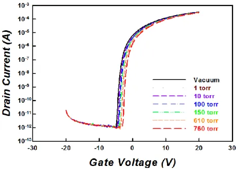
The device we use is without any passivation layer on α-IGZO TFT which means the back channel is exposed to atmosphere, Hence, we could discuss the relationship between the α-IGZO TFT and oxygen. The measurement procedure of each temperature as follow: First, we illuminate α-IGZO TFT at higher temperature in the vacuum chamber and the pump is always pumping at the same time to clean some part of the oxygen which is already absorbed on the α-IGZO TFT. The electrical characterization was carried out using Agilent 4156C Semiconductor Parameter Analyzer in a vacuum chamber system. Then, oxygen gas was fed into the chamber until the chamber pressure reached 1, 10, 100 and 760 torr as shown in Figure 4-2-1.
Figures 4-2-2 to Figure 4-2-5 show the VG-ID transfer curve of α-IGZO TFT at
273 K, 303 K, 333 K and 363 K respectively under the 0 (vacuum), 1, 10, 100, 760 torr oxygen ambient. Note that, the positive threshold voltage (VTH) shift which was
extracted by the method inchapter 3 is not obvious at the lower temperature while the threshold voltage (VTH) shift is apparent in the higher temperature as shown in Figure 4-2-6. It means that the oxygen of the atmosphere is easier absorbed on the channel of α-IGZO TFT at higher temperature. This would cause positive threshold voltage shift (VTH) of α-IGZO TFT. Because oxygen could capture an electron from
34
In addition, the subthreshold gate swing from Figures 4-2-2 to Figure 4-2-5 for each transfer VG-ID curve was extracted by the method which is already mentioned in
the chapter 3 as shown in Figure 4-2-7. Note that, the subthreshold swing does not show any trend with the partial pressure of oxygen increased at each temperature and variation among the range about 0.07 V/decade. The subthreshold swing can be associated with the density of deep bulk state (𝑁𝐵𝑆) and interface state at the interface between gate insulator and semiconductor layers (𝑁𝑆𝑆) by the following formula
(4.2.1): S. S. .3 𝐵
𝑞 𝑔 [ 𝑞 𝑖𝑛
𝜀𝑖𝑛 (√𝜀 𝑁𝐵𝑆 𝑞𝑁𝑆𝑆) (4.2.1)
where KB denotes the Boltzmann constant; T the temperature; q the elementary
electric charge; 𝜺𝒊𝒏𝒔 and 𝛆𝐬 are permittivity in insulator and semiconductor, respectively; and 𝒅𝒊𝒏𝒔 is the effective thickness of the insulator; [4.1] – [4.3]. The almost unchanged subthreshold swing means the density of state in the oxygen absorbed of α-IGZO is the same. However the formula (4.2.1) is an approximation method to estimate the average amount of density of state in α-IGZO subgap. The value of the density of state would be dominated by the maximum value among the subgap, this value doesn’t mean that all the density of state are the same in the α-IGZO subgap energy level. Hence we use another method to extract the density of state of α-IGZO under the condition which is oxygen absorbed on α-IGZO at different temperature.
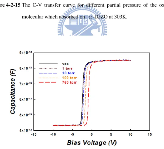
Reference shows the C-V measurement and numerical calculation method in which Kimura et al clamed to estimate the density of state in the subgap of α-IGZO
[4.4]. The C-V transfer curve is carried out using Agilent 4284A which the gate of the α-IGZO TFT is connected to Capacitance Measurement High (CMH) and the source and drain is connected to Capacitance Measurement Low (CML). Figure 4-2-8shows
35
the measured results of the C-V characteristic of α-IGZO TFT. Here the characteristics at applied frequency of 40 kHz which is the minimum value that we could get the capacitance value. It is observed that capacitance become small as the gate voltage bias below flat band voltage (VFB) because the electrons are depleted in
the α-IGZO film which means only the source and drain overlap capacitance detected. On the contrary, owing to the electrons are accumulated at the channel of the α-IGZO film, the capacitance become larger (overlap capacitance and channel capacitance) as gate voltage over flat band voltage
The trap densities were extracted using the following algorithm. First, the surface potential (ФS) is calculated from the C-V characteristic. By applying Q = CV to the
gate insulator, differentiating it by gate voltage, and transforming it, equations (4.2.2) and (4.2.3) are acquired. Moreover, by integrating equation (4.2.3) of gate voltage, equation (4.2.4) is acquired. Here, Ci is the geometrical capacitance of the gate
insulator of channel region, Cg is the measurement capacitance in the C-V
characteristic subtracts the source and drain overlap capacitance which means the minimum value of the C-V characteristic and VFB is the flatband voltage, which
corresponds to gate voltage where Cg begins to increase as shown red dash line in Figure 4-2-8. Q 𝐶 ∅ ) (4.2.2) ∂∅ ∂V𝐺 𝜕𝑄 𝜕𝑉𝐺 𝐶𝑖 𝐶𝑔 𝐶𝑖 (4.2.3) ∅ ∫ 𝐶𝑔 𝐶𝑖 𝑉𝐺 𝑉𝐹𝐵 (4.2.4)
Surface potential is a function of gate voltage. Figure 4-2-9shows the calculated result of the surface potential for α-IGZO TFT form C-V measurement. It is found that surface potentialis saturated at about 1 eV for high VG-VFB which indicates that
36
band edge approach the Fermi level as shown in Figure 4-2-10. Owing to the electrons are increased rapidly when the gate voltage larger than the threshold voltage, all the incensement of the gate bias above threshold voltage crossed over the gate insulator. Hence, the surface potential is no longer bending.
Next, we want to calculate the charge density in the channel layer by applying boundary condition and Poisson equation. Equation (4.2.5) is the boundary condition which means that the electric displacement is continuous between the vertical directions of gate insulator and semiconductor interface. Here, 𝜕∅ 𝜕 ⁄ is the surface potential gradient in the channel layer, 𝜖 is the dielectric constant of the gate insulator, 𝜖 is the dielectric constant of channel layer, and ti is the thickness of the
gate insulator. 𝜕∅ 𝜕𝑥 𝜖𝑖 𝜖 𝑉𝐺 ∅𝑆 𝑖 (4.2.5)
Equation (4.2.6) is the Poisson equation which means that the charge could determine the potential at each position alone the α-IGZO bulk direction. We would assume the charge is nearly the same in any position in the α-IGZO alone the α-IGZO bulk direction and the thickness of the α-IGZO is small so the integrate of equation (4.2.6) of each position is equation (4.2.7). Here, the d is the thickness of the α-IGZO. Note that, the gradient of potential in the α-IGZO at any position is the same so we could calculate from equation (4.2.5) and (4.2.7) to get the equation (4.2.8) which means the average charge density among the α-IGZO for each gate bias voltage (i.e. each surface band bending).
∂ ∅ ∂x ρ 𝜖 (4.2.6) 𝜕∅ 𝜕𝑥 ρ 𝜖 (4.2.7) 𝜌 𝜀 𝑉 ∅𝑆 ∙ 𝑖 (4.2.8)
37
Figure 4-2-11shows the calculation result of the channel charge as a function of gate bias voltage. Note that the charge density ρis saturate about 10-2 coulomb/cm3 which means the number of electron is 1017 #/cm3 when the gate voltage is 2V, this value consist with previous study result. On the contrary, there are tail state near the conduction band is about 1017~1018 cm-3 and deep state 1020 cm-3 which is 2.3 eV below the conduction band [4.5]. However the accumulation electron is only 1017 #/cm3 which means the relatively holes by gate bias is approximate this amount. When applied positive gate voltage Fermi level could be pinned near the conduction band owing to not too much electron could not fill this amount of density of state. On the other hand, when applied negative gate voltage Fermi level could be pinned at 2.3 eV below the conduction band due to the deep occupied state which is already full of electrons and it is not easy to exclude them.
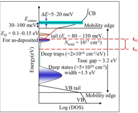
The charge density ρcontain localized trapped electron, free electrons… and so on. The localized trapped electron only related to the density of state according to the equation (4.2.9). Here, the N is density of state of α-IGZO subgap. So if differentiating the charge density ρby the potential among the subgap of α-IGZO, the density of state will be obtained as shown in Figure 4-2-12. Such C-V characteristic measurement range is among the subgap of α-IGZO where the interval of the red dash line as shown in Figure 4-2-13 so the density of state which we calculate is belonged to this interval.
∫ 𝑁∅ ∅ (4.2.9)
Figure 4-2-14 to Figure 4-2-17 show the C-V characteristic of α-IGZO TFT at 273 K, 303 K, 333 K and 363 K respectively under the 0 (vacuum), 1, 10, 100, 760 torr oxygen partial pressure and Figure 4-2-18 to Figure 4-2-21 show the result of density of state based on the Figure 4-2-14 to Figure 4-2-17 C-V characteristic
38
measurement by the method which is mention above. Note that, the density of state nearly unchanged when the oxygen absorbed on the α-IGZO under 273K and 303K while the density of state decrease when the oxygen absorbed on the α-IGZO under 333K and 363K. This means at higher temperature not only oxygen absorption easier but also oxygen could passivation the trap among the α-IGZO lead to the density of state which we calculated decreased.
To further confirm the oxygen absorbed on the α-IGZO could compensate trap of α-IGZO. We take two conditions into consideration. One is the α-IGZO TFT at 363 K under vacuum chamber; the other is also at 363 K under vacuum chamber but after the oxygen absorbed on the α-IGZO. The reason for the chamber temperature at 363 K is that according to the previous experiment the oxygen absorbed efficiently onα-IGZO at 363 K. Moreover, both conditions which measured in the vacuum chamber are for the purpose to exclude the field induced oxygen absorption on the α-IGZO to affect our measurement result. The capacitance of α-IGZO TFT was subject to back-to-back hysteresis loop sweeps VG = -5 to 4, -5 to 8, -5 to 12, -5 to 16
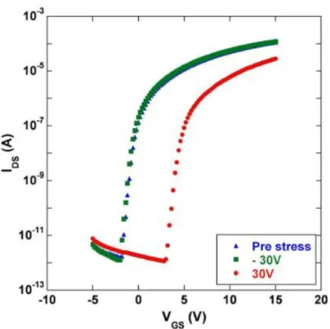
and -5 to 20 V which we fix the negative side at -5 V and vary positive side to consider the electron trapping effect. Here, we do not consider the negative bias side because it is not easy for α-IGZO TFT to inverse hole. From Figure 4-2-22, we observe that the flat band voltage (VFB) shift successively to more positive voltage for
each hysteresis loop during the return sweep. On the other hand, the device which the oxygen is already absorbed has lower flat band voltage (VFB) shift than the device
which is without oxygen absorbed. The flat band voltage (VFB) shift result from three
possible cases that electrons which are from α-IGZO TFT channel could be trapped: (1) in the bulk or back channel of α-IGZO TFT. (2) at the channel and dielectric interface. (3) injected into the dielectric. Due to the same device, the possible reason that could cause flat band voltage shift must not be electrons trapped at the channel
39
and dielectric interface or injected into the dielectric. Hence, the only one possible reason for the oxygen absorbed device which has lower flat band voltage (VFB) shift
under back to back sweep is the trap of α-IGZO decreased. As we sweep on the reverse loop, the Fermi level is from near conduction band to away conduction band. This would cause some electrons trapped in the α-IGZO trap lead to the higher flat band voltage (VFB) as show in Figure 4-2-23. Base on this model, the lower flat band
voltage shift means the lower trap of the oxygen absorbed α-IGZO. Therefore, we could conclude that the oxygen absorbed on the α-IGZO could compensate trap of α-IGZO.
40
Figure 4-2-1 The schematic of oxygen molecular fed into the measurement.
Figure 4-2-2 The I-V transfer curve for different partial pressure of the oxygen
41
Figure 4-2-3 The I-V transfer curve for different partial pressure of the oxygen
molecular which absorbed on α-IGZO at 303K.
Figure 4-2-4 The I-V transfer curve for different partial pressure of the oxygen
42
Figure 4-2-5 The I-V transfer curve for different partial pressure of the oxygen
molecular which absorbed on α-IGZO at 363K.
Figure 4-2-6 The threshold voltage (VTH) shift under different oxygen partial
43
Figure 4-2-7 The subthreshold swing (S.S.) shift under different oxygen partial
pressure at different temperature.
44
Figure 4-2-9 The surface potential as a function of gate voltage.
Figure 4-2-10 (a) The flat band condition (b) The maximum surface potential as
45
Figure 4-2-11 The maximum surface potential as a gate voltage larger than threshold
voltage.
46
Figure 4-2-13 The C-V detects range among two red dash lines. [4.8]
Figure 4-2-14 The C-V transfer curve for different partial pressure of the oxygen
47
Figure 4-2-15 The C-V transfer curve for different partial pressure of the oxygen
molecular which absorbed on α-IGZO at 303K.
Figure 4-2-16 The C-V transfer curve for different partial pressure of the oxygen
48
Figure 4-2-17 The C-V transfer curve for different partial pressure of the oxygen
molecular which absorbed on α-IGZO at 363K.
Figure 4-2-18 The density of state for different partial pressure of the oxygen
49
Figure 4-2-19 The density of state for different partial pressure of the oxygen
molecular which absorbed on α-IGZO at 303K.
Figure 4-2-20 The density of state for different partial pressure of the oxygen
![Figure 2.3.3 The Schematic diagram of water molecular donor elecrons to α-IGZO TFT. [2.29]](https://thumb-ap.123doks.com/thumbv2/9libinfo/8747566.205239/38.892.223.666.120.443/figure-schematic-diagram-water-molecular-donor-elecrons-igzo.webp)