國 立 交 通 大 學
電機與控制工程學系
碩
士 論 文
邊緣可適性即時數位影像放大硬體之
FPGA 實現
FPGA Implementation of Edge-Adaptive
Interpolation Hardware for Real-Time
Digital Image Resizing
研 究 生:羅儀晟
指導教授: 林進燈 博士
邊緣可適性即時數位影像放大硬體之
FPGA 實現
FPGA Implementation of Edge-Adaptive
Interpolation Hardware for Real-Time
Digital Image Resizing
研 究 生:羅儀晟
Student:Yi-Chen Lo
指導教授:林進燈
Advisor : Dr. Chin-Teng Lin
國立交通大學
電機與控制工程學系
碩士論文
A Thesis
Submitted to Department of Electrical and Control Engineering
College of Electrical Engineering
National Chiao Tung University
in Partial Fulfillment of the Requirements
for the Degree of Master
in
Electrical and Control Engineering
July 2008
邊緣可適性即時數位影像放大硬體之
FPGA 實現
學生:羅儀晟
指導教授:林進燈 博士
國立交通大學電機與控制工程研究所
中文摘要
近年來,消費性影像產品如:數位像機、數位攝影機、手機…等的普及率以 相當快的速度提升。相對的,在轉換影像解析度以及大小所用到影像補插法,其 重要性也是隨之上升;影像補插主要的目的在於由低解析度的影像產生高解析度 之補插影像。一些傳統的影像補插方法例如雙線性補插以及雙立方補插並不能滿 足高畫質之需求,因為這些方法可能會使影像模糊或者在影像邊緣產生鋸齒狀。 再者,高畫質高解析度影像放大所處理的影像資料量及運算量非常大,因此需要 使用硬體來加速運算之處理速度。 本論文實現了一個即時影像放大硬體,能夠對於一般標準數位視訊訊號作即 時性的放大。本論文採用即時影像補插方法的特色是:(1)決策模組能夠自動辨 別輸入影像之特徵將其分類,來決定影像補插模組之使用。當輸入影像對肉眼不 明顯時,選用雙線性補插方法以節省計算能耗,若輸入影像對肉眼明顯且具有方 向性時,為了減少在影像邊緣所產生之鋸齒狀以及模糊狀,則選用邊緣可適性影 像補插模組。(2)使用CORDIC 電路來運算反三角函數之解,大幅度省去為了近 似角度時使用查表所造成硬體的大量使用。 本論文所實現之即時影像放大硬體若操作在95Mhz 頻率狀態下,每秒能夠 處理約300張大小為CIF (320×240) 之影像,並且在影像品質方面有相當好的效 果,能夠有效的消除傳統影像補插法在影像邊緣產生鋸齒狀及模糊狀之缺點,對FPGA Implementation of Edge-Adaptive Interpolation
Hardware for Real-Time Digital Image Resizing
Student:Yi-Chen Lo Advisor : Dr. Chin-Teng Lin
Department of Electrical and Control Engineering
National Chiao Tung University
Abstract
In recent years, consumer digital image and/or video devices such as digital still cameras, digital video cameras, cell phones, etc, are more and more popular so that image interpolation becomes an increasingly important technology for image format/resolution conversion. The purpose of image interpolation is to transfer to a high resolution image from a low resolution image. Traditional interpolation schemes do not satisfy the requirement of high quality image due to jagged and blurry defects appearing in an edge. Besides, due to the large amount of computation of high resolution video data, it is necessary to accelerate the computation by using hardware.
In this thesis, a video scaling hardware is implemented on FPGA, and it can achieve real-time scaling up to standard digital video signal. The video scaling hardware has the following features. (1) It use fuzzy decision module to automatically identify the characteristic of input image and to decide which interpolation module will be used. If input image is not sensitive to human eyes, in order to reduce computational power, the bilinear interpolation module will be chosen. Otherwise, edge-adaptive image interpolation module will be selected to reduce blurry and jagged defects in edge section. (2) CORDIC circuit is used to replace arc tangent function which is used to calculate the orientations of input image. This method can effectively save hardware resources compared with a large look-up table.
In this thesis, the proposed FPGA design can achieve real-time video scaling processing in resolution of 320×240 (CIF image). While system frequency is at 95 MHz, the performance is above 300 frames per second. Compared with traditional image interpolation methods, the proposed FPGA design has better visual quality due to the reducing of blurry and jagged defects in edge section.
誌謝
兩年的研究所生涯隨著論文的完成劃上了句號,這兩年間,要感謝許多人的 鼓勵和幫忙,使我獲得充實的專業能力並順利完成研究所的學業。 首先要感謝的是我的指導教授-林進燈老師。林老師是國內十分傑出的一位 教授,在不同領域內都有相當好的研究成果。感謝老師提供了很理想的研究環 境、豐富的資源及正確的引導,使我在研究上非常順利。在老師悉心的指導下, 讓我學習到解決問題的能力及做研究應有的態度,使我獲益良多。還要感謝范倫 達教授時常關心我學業上的研究,時常與我討論論文方向及進度。以及特別感謝 蒲鶴章博士對於我研究上的指導,幫解決了我許多的問題。另外也感謝實驗室所 有的夥伴,經翔、德瑋、俊傑、靜瑩及智文等學長姐們。還有我的同學們,毓廷、 煒忠、建昇、孟修、寓鈞、舒愷、孟哲、俊彥、依伶。以及實驗室的學弟妹,昕 展、哲睿、介恩、家欣、有德,感謝大家在研究上及生活上的互相扶持及鼓勵。 最後要感謝家人爸爸、媽媽、妹妹的支持,讓我能專心於學術上的研究,渡 過所有難關,謝謝! 人生值得感謝的人其實很多,感謝老天、感謝許多親人、朋友和同學,在生 命的旅途中,因為有你們,因為我們彼此珍惜、相互扶持,才能有無比的力量。Contents
中文摘要...ii
Abstract... iii
誌謝...iv
Contents ...v
List of Figures ...vii
List of Tables...ix
Chapter 1 Introduction ...1
1.1 Motivation...1
1.2 Thesis Organization ...3
Chapter 2 Principle of Image Scaling and related research ...4
2.1 Basic Principle of Image Scaling...4
2.2 Several Traditional Interpolation Schemes ...7
2.2.1 Nearest Neighborhood ...7
2.2.2 Bilinear...9
2.2.3 Bicubic ...10
2.3 Defects of Traditional Interpolation Schemes ...12
2.4 HVS-Based Edge-Adaptive Image Scaling ...14
2.4.1 Introduction...14
2.4.2 Architecture...15
2.4.3 HVS-Directed Image Analysis...17
2.4.4 Image Interpolation Computation ...27
Chapter 3 Hardware Design of Edge-Adaptive Real-Time Image Scaling ...28
3.1 Introduction...28
3.2 Hardware Architecture...29
3.3 Data Flow Control Circuit ...31
3.4 Image Interpolation Circuit...34
3.4.1 Architecture...34
3.4.2 Fuzzy Decision Module ...35
3.4.3 Angle Evaluation Module ...41
3.4.4 Image Interpolation Module ...45
3.5 Input Image Acquisition Circuit ...48
3.5.1 ITU-R.656 Decoder ...48
3.5.2 Memory Address Generator Circuit for Frame Buffer Design ...51
3.6 Output and Timing Generator Circuit...56
Chapter 4 Experimental Results...57
4.2 FPGA Implementation...63
4.2.1 ITR-R.656 Signal Acquisition Unit ...64
4.2.2 Data Flow Control Unit ...65
4.2.3 Image Scaling Unit ...66
4.2.4 Output Timing and Data Address Generator Unit...67
4.2.5 Integration and Synthesis...68
4.2.6 Performance Estimation...69
4.2.7 Power Consumption...70
Chapter 5 Conclusions and Future Works...71
References...73
Appendix...76
A.1 Image Signal Formats ...76
A.1.1 Input Signal Format ...76
A.1.2 Output Signal Format...79
List of Figures
Fig. 1-1. SDTV and its resolution...1
Fig. 1-2. HDTV and its resolution. ...2
Fig. 2-1. Block diagram of signal reconstruction. ...4
Fig. 2-2. Ideal reconstruction filter. ...5
Fig. 2-3. Example of image scaling. ...7
Fig. 2-4. Time domain waveform of nearest neighborhood interpolation function...8
Fig. 2-5. Algorithm of nearest neighborhood interpolation scheme. ...8
Fig. 2-6. Time domain waveform of bilinear interpolation function. ...9
Fig. 2-7. Algorithm of bilinear interpolation scheme. ...10
Fig. 2-8. Time domain waveform of bicubic interpolation function...11
Fig. 2-9. Algorithm of bicubic interpolation scheme...11
Fig. 2-10. (a) Image enlarged by nearest neighborhood interpolation, (b) Image enlarged by bilinear interpolation, (c) original image. ...13
Fig. 2-11. Schematic block diagram of HVS-Based Edge-Adapted Image Scaling system....15
Fig. 2-12. (a) A 4 x 4 sliding (overlapping) block in original image, (b) The block after two times interpolation. [1]...16
Fig. 2-13. Visibility thresholds corresponding to different background luminance. [1]...18
Fig. 2-14. An illustration of the relation between SD parameter and the distribution of pixels in a sliding block. ...21
Fig. 2-15. Membership functions of fuzzy sets on input variables VD, SD, and CD...23
Fig. 2-16. Portions of four types of regions...24
Fig. 2-17. Flow diagram of angle evaluation...26
Fig. 2-18. Illustration of Dx and Dy in sliding block...26
Fig. 3-1. Video scaling method of our hardware. ...29
Fig. 3-2. Whole hardware of real-time HVS-based edge-adaptive video scaling...30
Fig. 3-3. Architecture inside FPGA development board...31
Fig. 3-4. Block diagram of data flow control circuit. ...32
Fig. 3-5. Fast memory loading working scheme...34
Fig. 3-6. Architecture of image interpolation circuit. ...35
Fig. 3-7. Modified computation flow of VD...36
Fig. 3-8. Experiment result of VD modification...37
Fig. 3-9. Modified SD computation flow...39
Fig. 3-10. Experiment result of SD modification.. ...39
Fig. 3-13. Architecture of CORDIC circuit. ...44
Fig. 3-14. Relation between input pixels and output pixels...46
Fig. 3-15. Experiment result of weights approximation. ...48
Fig. 3-16. Window used in ITU-R.656 decoder...49
Fig. 3-17. Operation method of finite state machine in ITU-R.656 decoder. ...50
Fig. 3-18. Separate Y from YCbCr data stream. ...52
Fig. 3-19. Scheme for checking if current input data is valid...52
Fig. 3-20. Working principle of Count_h...53
Fig. 3-21. Working principle of Count_v...54
Fig. 3-22. Mapping of input frame buffer and image capture window...55
Fig. 3-23. Architecture of output signal and timing generation circuit...56
Fig. 4-1. Experiment results of house image ...58
Fig. 4-2. Experiment results of car light image ...59
Fig. 4-3. Experiment results of jet fighter image ...60
Fig. 4-4. Experiment results of BW image ...61
Fig. 4-5. Demonstration platform. ...63
Fig. 4-6. Synthesis summary of ITU-R.656 signal acquire unit. ...64
Fig. 4-7. Timing report of ITU-R.656 signal acquire unit. ...64
Fig. 4-8. Synthesis summary of data flow control unit...65
Fig. 4-9. Timing report of data flow control unit...65
Fig. 4-10. Synthesis summary of image interpolation unit...66
Fig. 4-11. Post-simulation waveform of image interpolation unit...66
Fig. 4-12. Synthesis summary of output timing and data address generation unit. ...67
Fig. 4-13. Timing report of output timing and data address generation unit. ...67
List of Tables
Table 2-1. Experient results of fuzzy variables...25
Table 3-1. PSNR comparison of original and modified VD. ...38
Table 3-2. PSNR comparison of original and modified SD...40
Table 3-3. Relationship between Dx and Dy and Z. ...44
Table 3-4. States and their descriptions of Fig. 3-17. ...49
Table 3-5. Variables used to calculate memory address of input frame buffer. ...55
Table 4-1. PSNR comparison between each image interpolation method...62
Table 4-2. System performance while clock frequency is 95.73 MHz...69
Chapter 1
Introduction
1.1 Motivation
In recent years, consumer digital image and video devices such as digital still cameras, digital video cameras, cell phones, etc, are more and more popular so that image interpolation becomes an increasingly important technology for image format/resolution conversion in digital image processing. With the development of DTV broadcast and LCD HDTV, high resolution image can provide much more detailed information to satisfy the needs of users. Since the traditional video does not have the same resolution as HDTV, the images are needed to be scaled. For instance, the source signal resolutions are in traditional standard resolution of 720 x 480, but the HDTV LCD panel usually has higher resolution like 1920 x 1080. Fig. 1-1 and Fig. 1-2 show the difference between SDTV and HDTV.
Fig. 1-2. HDTV and its resolution.
If the video in SDTV resolution were played on HDTV, the resolution of the source signal should be enhanced in advance to fit the panel resolution of HDTV. For this reason, the quality to algorithm of resolution enhancement will affect visual performance enormously.
There are several kinds of methods to enhance image resolution, and the most famous are super-resolution reconstruction and image interpolation. The former extract one high resolution image from continuous low resolution images, although there are some differences between those low resolution images in space domain, but they have correlations in time domain, so we can reconstruct high resolution image by using approximating algorithm. However the image reconstruction algorithm needs a great amount of computation, so it is not suitable for practical applications. Another method is image interpolation which uses sampled data to convolute reconstruction filter function. It will reconstruct sampled data to un-sampled analog signal, and then re-sample the data finally. Common image interpolation functions are: nearest neighbor interpolation function, bilinear interpolation function, bicubic interpolation function. The quality of reconstructed signal will differ from which reconstruction
image losing high-frequency components, which are the edge sections of an image. Losing high-frequency components will let blur and jag appear on an image.
In order to have better visual quality, it should have advance image interpolation method to avoid blur and jag appear on interpolated images. The HVS-based edge-adaptive interpolation [1] has been proved to solve this problem effetely, and the algorithm is used in this thesis. An ideal interpolation scheme should always go along the edge so that this area will not blur and the smoothness will be preserved.
Since the data stream of video signal is quite large, we need to do lots of computation if we want to enhance the resolution of video signal by using advanced interpolation technique, and the memory used to store temporary video data must have high data transfer rate. Besides, video signal has its own regular input/output timing, so we only have restricted time to do computation of image interpolation. Since the advanced interpolation method requires lots of computation and is not able to be real-time in software simulation, if we want to do video resolution enhancement it in real-time, it is suitable to implement the video resolution enhancement hardware in ASIC or FGPA platform.
1.2 Thesis Organization
This Thesis is organized in as follows. Chapter 2 introduces the principal of image scaling, the defects of traditional image interpolation schemes and HVS-based edge-adaptive image scaling which is used in this thesis. Chapter 3 introduces our hardware of real-time video scaling and video spec. Chapter 4 is the experimental results of our HVS-based edge-adaptive image scaling and practical hardware
Chapter 2
Principle of Image Scaling and related research
2.1 Basic Principle of Image Scaling
Image scaling is also called image resizing and can be divided into scaling up and scaling down. In this thesis, we only discuss the situation of only scaling up, and scaling down situation is neglected. In fact, the principle of image scaling is sampling theorem of digital signal processing. It is mentioned that if we have samples of signal and the periodic of sampling, then we can recover original signal information, but aliasing is often generated while sampling the signal and this makes distortion to reconstructed signal. To avoid this situation, the sampling rate must be twice faster than signal rate when sampling signal, it is called nyquist sampling theorem. Fig. 2-1 is the block diagram of signal reconstruction and re-sampling, and it can explain the process of image resizing.
)
(
j
ω
H
r)
(n
f
Ideal reconstruct
f
r(t
)
filter
Sampling M
)
(n
f
mFig. 2-1. Block diagram of signal reconstruction.
The f(n) in Fig. 2-1 is a discrete sample of image signal, after f(n) passing ideal low pass filter, the reconstructed output signal from low pass filter is (2.1).
∑
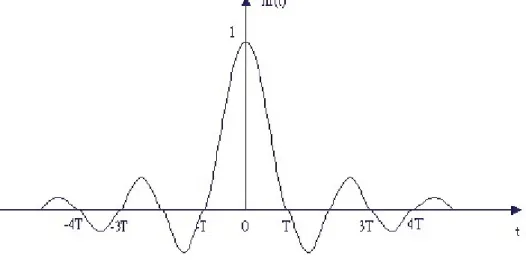
∞ −∞ = − = n nT t h n f t fγ( ) ( ) γ( ), (2.1)where T is sampling period of f(n), and hγ(t) is the impulse response of ideal
reconstruction filter withπ/T cut off frequency, and it can be expressed as (2.2).
T t T t t h / ) / sin( ) ( π π γ = . (2.2)
Figure 2-2 shows the ideal reconstruction filterhγ(t).
Fig. 2-2. Ideal reconstruction filter.
So the reconstructed continues signal can be expressed as (2.3).
∑
∞ −∞ = − − = n t nT T T nT t n f t f / ) ( ] / ) ( sin[ ) ( ) ( π π γ (2.3)reconstruction is the convolution of two functions, and the key point to the quality of reconstructed signal is the difference between different reconstruction functions. It is known that ideal reconstruction filter is sinc function, it a function with non zero value when time closing to infinite but not realizable in real application, so sinc function has to be replaced by other reconstruction functions. The quality of reconstructed signal will be different if we use different function to replace sinc function. To approximate perfect low pass filter and have least distortion, many interpolation schemes use piecewise function to replace sinc function. Piecewise function uses different functions in different temporal sections. Sinc function is symmetrical when time is zero, so the functions which are used to replace sinc function usually have same characteristic.
The goal of re-sampling in Fig.2-1 is to make continues signal fγ(t) back to
discrete digital signal and can be expressed as (2.4),
) ( ) ( M T f n fm = γ , (2.4)
where M is to coefficient of sampling, if M > 1 means that it samples more data and that will enlarge output image, if M = 1 means that the size of output image remains unchanged, if 0 < M < 1 means the size of output image becomes smaller.
Figure. 2-3 shows an example of image scaling up action. In the left is the original image and output image is the image in the right side.
Fig. 2-3. Example of image scaling.
We will introduce several traditional interpolation functions and discus their advantages and disadvantages in next section.
2.2 Several Traditional Interpolation Schemes
2.2.1 Nearest Neighborhood
Nearest neighborhood interpolation scheme is the simplest and most efficient interpolation function, it has very low computational complexity but has poor image quality. During it process Image scaling, it usually generates jagged and blocking. Its mathematical function can be expressed as (2.5) and the waveform of time domain is shown in Fig. 2-4. ⎪ ⎧ − < < t 1 1 , 1 Scaling Up
Fig. 2-4. Time domain waveform of nearest neighborhood interpolation function.
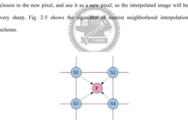
The algorithm of this interpolation scheme is to identify which original pixel is closest to the new pixel, and use it as a new pixel, so the interpolated image will be very sharp. Fig. 2-5 shows the algorithm of nearest neighborhood interpolation scheme.
Fig. 2-5. Algorithm of nearest neighborhood interpolation scheme.
In Fig. 2-5, P is the new pixel that needed to be interpolated, and S1, S2, S3 and S4 are original pixels. If S4 is closest to P, then we use S4 as P in interpolated image.
2.2.2 Bilinear
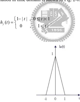
Bilinear interpolation is popular in many applications, although it is more complex than nearest neighborhood interpolation, but the quality of its result is much better than the result of NN interpolation. Its computation time is longer than NN interpolation due to the interpolated pixel needed to be calculated. The main disadvantage of bilinear interpolation is that it usually generate blur and jag in the edge section. The function of bilinear interpolation is as (2.6) and the waveform of bilinear interpolation in time domain is shown in Fig. 2-6.
⎩ ⎨ ⎧ < < ≤ − = | | 1 , 0 1 | | 0 , | | 1 ) ( t t t t hγ . (2.6)
Fig. 2-6. Time domain waveform of bilinear interpolation function.
Bilinear interpolation works in 2-dimension space, and 1 interpolated pixel is decided by 4 sampled pixels, the algorithm of bilinear interpolation scheme is shown
Fig. 2-7. Algorithm of bilinear interpolation scheme.
As we can see in Fig. 2-7, P is the new pixel needed to be interpolated, and S1, S2, S3 and S4 are original pixels. If an original pixel is closer to P, and the weight of this original pixel to P will be higher, otherwise it will be smaller. In Fig. 2-7, dx and dy are the distances from P to S1, S2, S3 and S4, x and y are the distances between original pixels. Bilinear interpolation scheme can be expressed as (2.7).
) )( ( ) )( ( ) )( ( ) )( ( y dy x dx S y dy x dx x S y dy y x dx S y dy y x dx x S P= − − + − + − + (2.7)
2.2.3 Bicubic
Bicubic interpolation is somewhat like bilinear interpolation, and the interpolation core of bicubic interpolation is more similar to sinc function than bilinear interpolation is. Bicubic interpolation uses near-by 16 pixels to compute interpolated pixels, so it is not as efficiency as bilinear interpolation. The result of bicubic interpolation is better than previous two interpolation schemes, but the
disadvantages of bicubic interpolation are that there is still blur in edge part and large amounts of computation. Mathematical function of bicubic interpolation is shown as (2.8), and the waveform of bicubic interpolation in time domain is shown in Fig. 2-8.
⎪ ⎩ ⎪ ⎨ ⎧ ≤ < ≤ − + − < ≤ − = | | 2 , 0 2 | | 1 , | | | | 5 | | 8 4 1 | | 0 , | | 1 ) ( 2 3 t t t t t t t t hγ (2.8)
Fig. 2-9 shows the algorithm of bicubic interpolation scheme, where P is the new pixel needed to be interpolated, and S( ji, ) are original pixels S1 ~ S16, W( ji, ) are weights of S1 ~ S16. P is calculated by summing the products of S1 ~ S16 with their weights and it can be expressed as (2.9).
∑∑
= = = 4 1 4 1 ) , ( * ) , ( i i j i W j i S P (2.9)2.3 Defects of Traditional Interpolation Schemes
The image quality will change if we use different schemes to do interpolation, so we will discuss the defects of nearest neighborhood interpolation scheme and bilinear interpolation scheme in this section. The common defects in interpolated images are as below.
(1) Blur
If blur occurs in an image, it will be hard to focus or identify the object in an image, and the quality of image is reduced. The occurring of blur is because that the reconstruction filter is usually a low pass filter, and low pass filter will filter high frequency parts of signal. In image signal, high frequency parts are usually in edge section. Therefore, if we filter high pass parts of image signal, the information of edge section will be lost. We use bilinear interpolation as an illustration, Fig. 2-10 (b) is an image enlarged by bilinear interpolation, and we can find blurry defects in this image.
(2) Block & Jag
In real interpolation application, data is sampled in finite quantity, and the pixel of sampling point will be affected by near-by pixels and this cause jag appearing in edge sections of image. The effect of block and jag will be more obviously if the time domain waveform curve of interpolation function is more oblique. We use nearest neighborhood interpolation as an illustration, Fig. 2-10 (a) is an image enlarged by nearest neighborhood interpolation, and it contains obvious block and jag in edge section.
Fig. 2-10. (a) Image enlarged by nearest neighborhood interpolation, (b) Image enlarged by bilinear interpolation, (c) original image.
2.4 HVS-Based Edge-Adaptive Image Scaling
2.4.1 Introduction
It has been known that conventional interpolation techniques such as the bilinear and the bicubic interpolations do not satisfy the requirement of high quality image since these methods tends to some obvious defects such as blur and jag. Recently, several adaptive nonlinear methods have been proposed to tackle these problems. In these methods, the image is analyzed at first to achieve better interpolation quality [2]-[5].
Since human eyes are more sensitive to the edge areas than smooth areas within an image, many algorithms [6]-[16] have been proposed to improve the subjectively visual quality of edge regions in the images that need to apply interpolation. However, how to design the optimal-adaptive filter and how to judge the quality of interpolated images are the challenges for these methods.
To avoid the disadvantage of conventional interpolation, this thesis use HVS-based edge-adaptive image scaling scheme [1]. This image interpolation method combines the bilinear interpolation and an edge-adaptive image interpolation. By using a fuzzy decision system [17], [18] inspired by the human visual system to classify the input image into human perception non-sensitive regions and sensitive regions to determine either the bilinear interpolation module or edge-adaptive interpolation module is selected to operate for each region.
2.4.2 Architecture
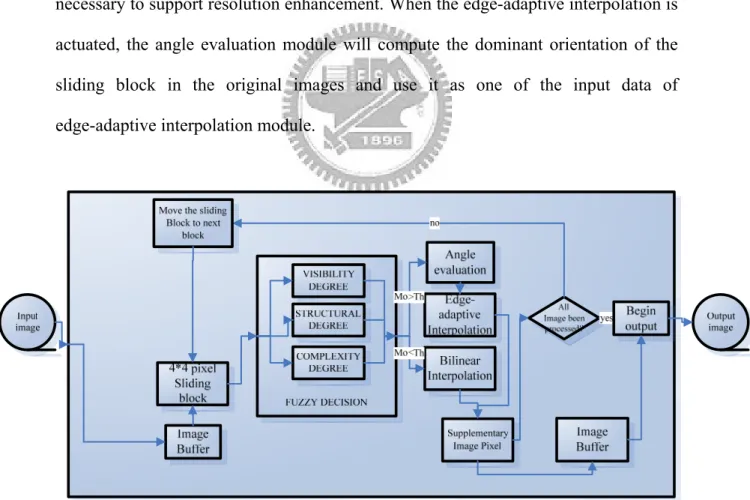
The schematic block diagram of HVS-based edge-adaptive image scaling scheme is shown in Fig. 2-11. This scheme consists of a fuzzy decision module, an angle evaluation module, an edge-adaptive interpolation module and a bilinear interpolation module. Fuzzy decision module designates each sliding block as shown in Fig. 2-12; it receives for one of a plurality of predefined classifications. Based on this classification, one of the bilinear interpolation and edge-adaptive interpolation modules is selected for actuation in generating the supplementary image pixels necessary to support resolution enhancement. When the edge-adaptive interpolation is actuated, the angle evaluation module will compute the dominant orientation of the sliding block in the original images and use it as one of the input data of edge-adaptive interpolation module.
(a) (b)
Fig. 2-12. (a) A 4 x 4 sliding (overlapping) block in original image, (b) The block after two times interpolation. [1]
When an original image enters our system, it is firstly divided into 4 x 4 sliding (overlapping) blocks. In other words, an image is constructed by many overlapped sliding blocks. The block is shown in Fig. 3-2 as an illustration, where O( ji, ) are the pixels of the original image and P(1,0), P(0,-1), P(1,-1) are the pixels needed to be interpolated in current block for 2 times interpolation. The weighted interpolation is used and can be presented as (2.10),
∑∑
= = = 3 0 3 0 , , ( , ) ) , ( ) , ( i j n m i j W j i O n m P θ (2.10)where the weights Wθ,m,n(i, j) are derived from edge-adaptive interpolation module, it will be introduced in later section.
2.4.3 HVS-Directed Image Analysis
It is well known that classical linear interpolation techniques often suffer from blurring edges or introducing artifacts around edges. An ideal interpolation scheme should always go alone the edge orientation because it would not blur the edge and well preserve the smoothness along the edge orientation.
In order to achieve optimal edge-directed interpolation, we make use of the properties of the human visual system to be our foundation by which we procure the futures of images. We could also realize which region would be worth processing for us in particular by using the properties of HVS, since human eyes would be usually more sensitive to this region.
1. Fuzzy Decision
Researches have been made on the characteristics of human visual system (HVS). It was found that the perception of HVS is more sensitive to luminance contrast rather than uniform brightness. The ability of human eyes to tell the magnitude difference between an object and its background depends on the average value of background luminance. As shown in Fig. 2-13, visibility threshold is lower when the background luminance is within the interval from 70 to 150, and the visibility threshold will increase if the background luminance becomes brighter or darker away from this interval. In addition, high visibility threshold will occur when the background luminance is in very dark region [19].
Fig. 2-13. Visibility thresholds corresponding to different background luminance. [1]
In addition to the magnitude difference between object and the background, different structures of images also cause different perceptions for HVS. Human eyes are more sensitive to high contrast regions such as texture or edge regions than the smooth regions. Since we have to make a balance between image quality, processing speed and power consumption, in our interpolation method, a novel fuzzy decision system inspired by HVS is used to classify the input image into human perception non-sensitive regions and sensitive regions. For non-sensitive regions, the bilinear interpolation module is used to reduce the power consumption. For sensitive regions, the edge-adaptive interpolation module is used to archive better visual quality.
There are three input variables in our fuzzy decision system, visibility degree (VD), structure degree (SD) and complexity degree (CD). VD is used to check if the object in the sliding block can be easily seen by human eyes, SD and CD are used to
check if image in sliding block have characteristic of edge structure. The fuzzy decision system has an output that which interpolation module should be used. We will introduce fuzzy decision system in detail in fellow five sub-sections.
(1) Visibility degree
In order to obtain the input variables corresponding to each sliding block, two index parameters should be calculated at first. Parameter background luminance (BL) [19] is the average luminance of the sliding block and can be calculated by (2.12).
BL=
∑∑
= = × 3 0 3 0 ) , ( ) , ( 23 1 i j j i B j i O , (2.11) Where ⎥ ⎥ ⎥ ⎥ ⎦ ⎤ ⎢ ⎢ ⎢ ⎢ ⎣ ⎡ = 1 1 1 1 1 2 2 2 1 2 0 2 1 2 2 2 ) , ( ji B . (2.12)Parameter D is the difference between the maximum pixel value and the minimum pixel value in the sliding block and can be calculated by (2.13).
)) , ( min( )) , ( max(O i j O i j D= − (2.13)
BL BL e
e BL
V( )=20.66 −0.03 + 0.008 . (2.14)
After BL, D and V(BL) are obtained, we can calculate the input variables (VD, SD and CD) of the fuzzy decision system. Parameter VD is defined as the difference between D and V(BL) and can be represented as (2.15).
) (BL V D
VD= − . (2.15)
If VD > 0, it means the magnitude difference between the object and its background exceeds the visibility threshold and the object is sensible. Otherwise, this object is not sensible.
(2) Structure degree
SD shows if the sliding block is a high contrast region and the pixels in the block can be obviously separated into two clusters. It is calculated by (2.16).
[
]
)) , ( min( )) , ( max( )) , ( min( )) , ( ( )) , ( ( )) , ( max( j i O j i O j i O j i O mean j i O mean j i O SD − − − − = (2.16) where∑∑
= = = 3 3 0 ) , ( 16 1 )) , ( ( o i j j i O j i O mean (2.17)An illustration of (2.16) is shown in Fig. 2-14. According to Fig. 3-4, if we makeσ =max(O(i, j))−mean(O(i, j)),σ =mean(O(i, j))−min(O(i, j)), (2.16) can
be expressed by (2.18). ) ( 1 2 2 1 σ σ σ σ + − . (2.18)
Fig. 2-14. An illustration of the relation between SD parameter and the distribution of pixels in a sliding block.
So the SD can be normalized to [0, 1]. If SD is small (close to zero) and σ1 and
2
σ are close [as Fig. 2-14(a)], it means that pixels in the block can be separated into two even clusters. The block may contain edge or texture structure. On the contrary, if SD is a large value (σ1 −σ2 >>0) [as Fig. 2-14(b)], it means that pixel number of
one cluster and that of the other cluster are not even; thus, the block may contain noise.
(3) Complexity degree
calculated by (2.19).
∑∑
= = − + + + − + + − = 3 0 3 0 )] 1 , ( ' ) 1 , ( ' ) , 1 ( ' ) , 1 ( ' [ ) , ( ' 4 i j j i O j i O j i O j i O j i O CD (2.19)Where O'(i,j) is the binarized version of input to eliminate the influence of image intensity. Each pixel in the 4 x 4 sliding block takes the four-directional local gradient operation, and the CD is the summation of the 16 local gradient values. If the CD is a large value, it means the block may contain texture structure. On the contrary, if the CD is a small value, the block may contain delineated edge structure.
(4) Fuzzy output
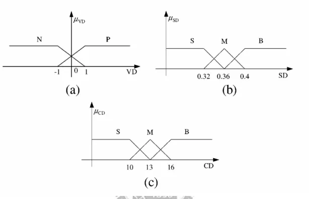
Variable VD has two fuzzy sets, N(negative) and P(positive), variable SD has three fuzzy sets, S(small), M(medium) and B(big), variable CD also has three fuzzy sets, S(small), M(medium) and B(big). The membership functions corresponding to the VD, SD, and CD are shown in Fig. 2-15 (a)–(c), respectively. Seven fuzzy decision rules are used in fuzzy decision system and represented as follows:
1. If VD is N then Mo is BL. 2. If SD is B then Mo is BL. 3. If CD is B then Mo is BL.
4. If VD is P and SD is S and CD is S then Mo is AA. 5. If VD is P and SD is S and CD is M then Mo is BL. 6. If VD is P and SD is M and CD is S then Mo is AA.
When the output of fuzzy decision system is AA, system will choose edge-adaptive interpolation module, otherwise the bilinear interpolation module would be used.
Fig. 2-15. Membership functions of fuzzy sets on input variables VD, SD, and CD.
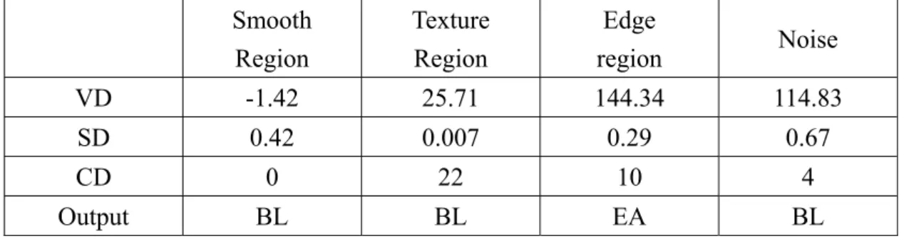
(5) Experiment of Fuzzy Input Variables
Fig. 2-16 shows four different image structures to illustrate the operations of the fuzzy decision system. Fig. 2-16 (a)–(d), represents smooth, texture, edge, and noise regions, respectively. The VD, SD, and CD values of these regions are shown in Table 2-1.
According to the VD values in Table 3-1, only Fig. 2-16 (a) (smooth region) is negative, which activates fuzzy rule 1 and follows the assumption that “if VD >0, it
activates fuzzy rule 2 and follows the assumption that “If SD is a large value, the block may contain noise." The SD values of Fig. 2-16 (b) (texture region) and Fig. 2-16 (c) (edge region) are small (S), which follows our assumption that “if SD is small, the block may contain edge or texture structure. The CD value of Fig. 2-16 (b) is medium (M), which activates fuzzy rules 5 and it follows the assumption that “If CD is a large value, the block may contain texture structure." The CD value of Fig. 2-16 (c) is small (S), which activates fuzzy rule 4 and follows the assumption that “If CD is a small value, the block may contain edge structure."
Table 2-1. Processing results of the fuzzy decision system corresponding to three different structures shown in Fig. 2-16.
Smooth Region Texture Region Edge region Noise VD -1.42 25.71 144.34 114.83 SD 0.42 0.007 0.29 0.67 CD 0 22 10 4 Output BL BL EA BL
2. Angle Evaluation
According to Fig. 2-11, when fuzzy decision module selects edge-adaptive interpolation module, angle evaluation is performed to determine the dominate orientation of the sliding block. The flow diagram of angle evaluation is shown in Fig. 2-17. When angle evaluation is operating, the orientation angle of each neighborhood original image pixel is computed. According to Fig. 2-12, when the orientation angle of O( ji, ) denoted as A( ji, ) is computed, the luminance values of the original pixels nearby O( ji, ) are used for the following computations as (2.20)-(2.21), and we use Fig. 3-8 to illustrate (2.20) and (2.21).
)) 1 , 1 ( ) , 1 ( 2 ) 1 , 1 ( ( ) 1 , 1 ( ) , 1 ( 2 ) 1 , 1 ( ) , ( + + + + + − + − + − + − + − − = j i O j i O j i O j i O j i O j i O j i Dx (2.20) )) 1 , 1 ( ) 1 , ( 2 ) 1 , 1 ( ( ) 1 , 1 ( ) 1 , ( 2 ) 1 , 1 ( ) , ( + + + + + + − − − + + − + − − = j i O j i O j i O j i O j i O j i O j i Dy (2.21) )] ) , ( ) , ( ( [tan 180 ) , ( 1 j i Dx j i Dy j i A =− − π (2.22) where ≤ i≤ , ≤ j≤ .
Fig. 2-17. Flow diagram of angle evaluation.
Fig. 2-18. Illustration of Dx and Dy in sliding block.
The obtained orientation angle of each neighborhood original image pixel is quantized into eight quantization sectors such as θ =22.5×k degrees, where k=0, 1… 7. The system will gather the most frequently occurring quantized orientation and send into edge-adaptive interpolation module.
2.4.4 Image Interpolation Computation
If the output of fuzzy decision module is BL, it means that the input image is not edge structure, so we just simply use bilinear interpolation to interpolate the image. On the contrary, when fuzzy decision outputs AA, it means that current image input has edge structure, and needed to be interpolated by edge-adaptive interpolation module. Angle evaluation module will calculate the dominate orientation of the input image, and send the orientation information to edge-adaptive module for weight generation. In (2.10), Wθ,m,n(i, j) are the weights corresponding to the orientation of input image. Weights will differ from different orientation and the location that needed to be interpolated. Weighting matrix Wθ,m,n(i,j) can be represented as follow:
. (2.23)
Three interpolated pixels will be generated from one sliding block, generating one interpolated pixel need 16 weights, so a sliding block need 48 weights to complete interpolation of three pixels. To reduce system complexity, all weights are pre-trained by back propagation neural network and saved in a table.
Chapter 3
Hardware Design of Edge-Adaptive
Real-Time Image Scaling
3.1 Introduction
With the development of DTV broadcast and LCD HDTV, high resolution image can provide much more detailed information to satisfy the needs of users. Since the traditional video does not have the same resolution as HDTV, the images are needed to be scaled. For instance, the source signal resolutions are in traditional standard resolution of 720 x 480, but the HDTV LCD panel usually has higher resolution like 1920 x 1080. If the video in SDTV resolution were played on HDTV, the resolution of the source signal should be enhanced in advance to fit the panel resolution of HDTV.
Due to the data stream of video signal is quite large, we need to do lots of computation if we want to enhance the resolution of video signal by using advanced interpolation technique, and the memory used to store temporary video data must have high data transfer rate. Because video signal has its own regular input/output timing, so we only have restrict time to do computation of image interpolation. If we want to make video resolution enhancement in real-time, it is suitable to implement the video resolution enhancement system in ASIC or FGPA platform [20]-[26].
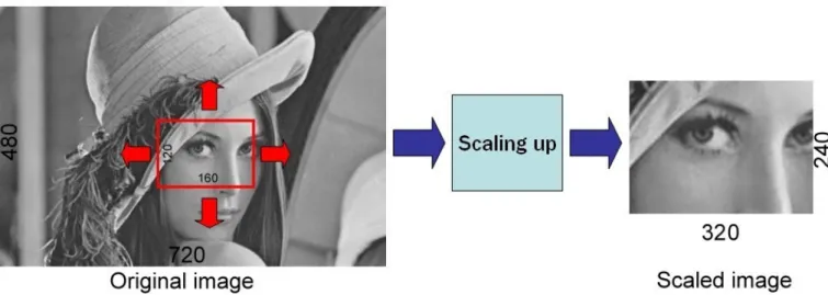
In order to verify our edge-adaptive image interpolation hardware can operate in real-time, we have designed a real-time HVS-based edge-adaptive video scaling hardware. The ITU-R.656 standard input signal is provided by video decoder, and the
resolution of input signal is 720 x 480 pixels. Our hardware outputs scaled video signal to LCD monitor with resolution of 320 x 240.
Fig. 3-1. Video scaling method of our hardware.
The method of video scaling in our hardware is shown in Fig. 3-1. At beginning, we capture an image from input video frame, and the size of capturing window is 160 x 120. After input image acquiring, the hardware will enhance resolution of input image in factor of 2, the output image resolution will be 320 x 240, and then the processed image will be output to LCD monitor for observation. It will have no flexibility if the location of capturing window is fixed in some specific area. In our hardware, user can freely control the movement of capturing window through the push bottoms on FPGA development board.
3.2 Hardware Architecture
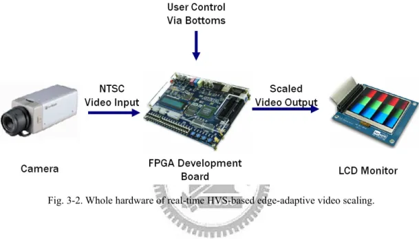
Figure 3-2 shows whole hardware of real-time edge-adaptive video scaling. Our hardware is based on Altera FPGA development board, this development board has
Device, this video decoder can receive analog video signal such as NTSC, PAL and SCREAM and outputs ITU-R.656 standard digital video data stream. We connect a LCD monitor to FPGA development board through GPIO interface and user can directly observe the result of scaled image by watching LCD monitor. Besides, users are able to control our hardware through switches and bottoms on the board.
Fig. 3-2. Whole hardware of real-time HVS-based edge-adaptive video scaling.
Figure 3-3 shows the architecture inside FPGA development board. After ADV7180 transform analog NTSC signal into ITU-R.656 standard digital data stream, the digital data stream needs to be decoded by ITU-R.656 decoder, and capture the image block which we want to interpolate into input frame buffer for following computation. Data flow control unit is responsible for data transition from one function unit to another, it read the data that needed by scaling circuit from input frame buffer and transfer them to scaling circuit and output frame buffer in the same time. Output data address and timing generation circuit generate timing information for LCD monitor and corresponding data address in output frame buffer. Finally, the interpolated image data is sent to LCD monitor through GPIO interface.
Fig. 3-3. Architecture inside FPGA development board.
3.3 Data Flow Control Circuit
After input image capturing is complete, data flow control circuit takes charge of data transmission between input frame buffer, output frame buffer and image interpolation circuit. Block diagram of data flow control circuit is shown in Fig. 3-4, and its operating methods are as below.
1. Before input image capturing is complete, the status of circuit is Wait_for_start and does nothing.
2. After input image capturing is complete, input image acquiring circuit will inform data flow control circuit and data flow control circuit will change to next status, and it takes one cycle to complete this action.
3. When circuit starts working, it will firstly enter Load_mem_36 stage. Image interpolation circuit needs 36 input registers, so we have to fill them with
location of image data in output frame buffer according to its location in input frame buffer, then store image data to output frame buffer. This action can save time to store data from registers. It takes 37 cycles to finish this stage.
4. After all data needed by image interpolation circuit are loaded, the status changes to compute stage. In this stage, image interpolation circuit use 36 input data to compute the corresponding answer. When the computation is finished, image interpolation circuit will send generated pixels to data flow control circuit. The numbers of cycles to finish this stage is according to different clock cycle time because the time period of computation is fixed and have nothing to do with clock cycle time.
5. When computation is over, data flow control circuit calculates their address in output frame buffer according to the address of input data and store them into output frame buffer. It takes three cycles to finish this stage.
6. After interpolated pixels are stored into output frame buffer, data flow control circuit will identify current position of sliding block. If all input image data is processed, status will back to Wait_for_start stage; Else if sliding block is on the right border, status changes to Load_mem_36 stage and load data needed by next sliding block; Else if sliding block is not on the border of image, status will changes to Load_mem_6 status.
7. If sliding block is not on the right border of image, then it is overlapped with next sliding block, there will be 30 pixels the same as next sliding block. It will waste too much time if we load all 36 pixels from input frame buffer; it takes 37 cycles to load 36 pixels. So we use Load_mem_6 in this situation, this stage change positions of 30 pixels in input registers, and the other pixels are loaded from input frame buffer. Fig. 3-5 shows how Load_mem_6 works, and it takes only 7 cycles to finish loading operation. This action boosts hardware performance from 112 FPS to 300 FPS.
Fig. 3-5. Fast memory loading working scheme.
3.4 Image Interpolation Circuit
3.4.1 Architecture
Fig. 3-6 shows the architecture of image interpolation circuit, the inputs of this circuit are 36 pixels image data and the outputs are three interpolated pixels. There are three modules in this circuit, fuzzy decision module, angle evaluation module and image interpolation module. Fuzzy decision module will identify characteristics of input image data and evaluate if current input is worthy of using edge-adaptive interpolation. Angle evaluation module estimate dominate orientation of input image. The result of fuzzy decision module and angle evaluation module will be sent to image interpolation, then choosing interpolation method and calculate output data.
Fig. 3-6. Architecture of image interpolation circuit.
3.4.2 Fuzzy Decision Module
There are three sub-modules in fuzzy decision module, visibility degree module (VD), structure degree module (SD) and complexity degree module (CD). These modules identify the characteristics of input image and evaluate that if input image is sensitive to human eyes, if the answer is true, use edge-adaptive interpolation, otherwise use bilinear interpolation.
(1) Visibility Degree Module
In original adaptive image scaling algorithm, variable VD is calculated by (3.1).
) (BL V D VD= − (3.1) where )) , ( min( )) , ( max(O i j O i j D= − (3.2) BL BL e e BL V( )=20.66 −0.03 + 0.008 (3.3)
V is sum of two exponential functions, and they are not simple exponential function, so it is difficult to implement them in hardware because of high complexity and overusing resource. In order to overcome this problem, VD must be approximated; Fig. 3-7 shows modified computation flow of VD.
Original VD use the comparison between luminance difference and the variable visibility threshold to identify if object is visible, and we can fix the visibility threshold to a proper value. What we have to do is comparing luminance difference with the fixed visibility threshold [20]. Since visibility threshold is fixed, the condition of luminance difference exceeding visibility threshold is slightly reduced.
Fig. 3-8. Experiment result of VD modification. (a) difference, (b) original VD, (c) modified VD.
Fig. 3-8 shows the experiment result of modified VD, the difference between (b) and (c) mostly occurs in smooth region, only very few of them occur in edge region.
(a)
Table 3-1. PSNR comparison of original and modified VD. Original VD Modified VD
PSNR 27.742 dB 27.598 dB
(2) Structure Degree Module
In original edge-adaptive image scaling algorithm, variable VD is calculated by (3.4).
[
]
)) , ( min( )) , ( max( )) , ( min( )) , ( ( )) , ( ( )) , ( max( j i O j i O j i O j i O mean j i O mean j i O SD − − − − = (3.4)In (3.4), the result of SD will locate between zero to one, we can not use decimal fraction unless using floating point computation, but that will cost too much resource and processing time to use floating point computation. Besides, original SD computation contains division, and this makes lower circuit speed and higher resource usage. Due to several reasons mentioned above, variable SD must be modified.
As mentioned in previous, SD can be normalized to [0, 1], that is when the answer of (3.4) is larger than 0.5, SD is set to 1, otherwise SD is set to 0. The denominator and the numerator of (3.4) are both 8-bit fix-point integers, when we want to know if (3.4) is larger than 0.5, we can just do comparison between [7:1] bits of denominator and [6:0] bits of numerator, if [7:1] bits of denominator is larger than [6:0] bits of numerator, it means that (3.4) is small than 0.5, so we set output of SD module to 0, otherwise output of SD is 1. After modifying, the complexity of computing variable SD is reduced substantially, and the modified computation flow is shown in Fig. 3-9.
Find Mean Find Max data
Input image data
Find Min data
Max-Mean-(Mean-Min) Max+Min ABS circuit Right Shift 1 Bit Compare Structure Degree
Fig. 3-9. Modified SD computation flow.
(a)
(b)
(c)
Fig. 3-10. Experiment result of SD modification. (a) difference, (b) original VD, (c) modified VD.
Table 3-2. PSNR comparison of original and modified SD. Original SD Modified SD
PSNR 27.742 dB 27.615 dB
(3) Complexity Degree Module
Because of the computations in variable CD are all simple integer computations, so we don't have to modify the computation of CD. But there is a threshold circuit in this computation, if the data reach the threshold, the circuit will output 1 as answer, and otherwise the answer will be 0. We use adaptive thresholding to binarize pixels into 0 and 1. The result of adaptive thresholding is mean value of pixels in sliding block. We use the outputs of threshold circuit to do computation in (2.19) then get the result of variable CD. Fig 3-11 shows full architecture of fuzzy variables computation circuit.
3.4.3 Angle Evaluation Module
The principle of angle computation in angle evaluation module is sobel operator, in (3.5) ~ (3.7), Dx and Dy only use normal integer additions an subtractions, but when (4.7) use Dx and Dy to compute angle information, it also use arc tangent function, besides, this arc tangent function contains a division Dx/Dy. If we use look up table to find the angle information of Dx and Dy, it will cost too much hardware resource and make complexity too high.
Therefore, we adopt CORDIC circuit to estimate angle information by using Dx and Dy. After all, a sliding will generate 16 angle information, and we have to find out which angle appear most frequently and set this angle as output of angle evaluation module. )) 1 , 1 ( ) , 1 ( 2 ) 1 , 1 ( ( ) 1 , 1 ( ) , 1 ( 2 ) 1 , 1 ( ) , ( + + + + + − + − + − + − + − − = j i O j i O j i O j i O j i O j i O j i Dx (3.5) )) 1 , 1 ( ) 1 , ( 2 ) 1 , 1 ( ( ) 1 , 1 ( ) 1 , ( 2 ) 1 , 1 ( ) , ( + + + + + + − − − + + − + − − = j i O j i O j i O j i O j i O j i O j i Dy (3.6) )] ) , ( ) , ( ( [tan 180 ) , ( 1 j i Dx j i Dy j i A =− − π (3.7)
(1) CORDIC Module
functions. Comparing to huge look up tables, CORDIC circuit can calculate many functions by only using shifter, adder, subtract, and a very small look up table.
Fig. 3-12 shows how CORDIC operates, CORDIC uses approaching technique to find the answer. In Fig. 3-10, if β is 56.25 degrees and we want find β. We start from V0 which is 0 degree, and current angle is smaller than β, so we add 45 degrees to V0 and become V1. At V1, current angle is still smaller than β, so we add 22.5 degrees to V1 and become V2. At V2, current angle becomes larger than β, so we have to subtract 11.25 degrees and become V3, and V3 is exact on β which we desired for.
Fig. 3-12. CORDIC operating principle.
Now we explain CORDIC in mathematic aspect, in (3.8), x and y change while β rotate θ degrees. ) sin( ) cos( ' ) sin( ) cos( ' θ θ θ θ x y y y x x + = − = (3.8)
If we take out cos(θ) in (3.8), it will become (3.9), we have not done any simplified action at this step.
)) tan( )( cos( ' )) tan( )( cos( ' θ θ θ θ x y y y x x + = − = (3.9)
If we restrict rotation angle θ and maketan(θ)= 2± −i, the multiplications of tan(θ)
in (3.9) can be replaced by simple shift operations.
(3.10) is iterative rotations of CORDIC and is modified from (3.9), where di is 1 ± and Ki is constant. ) 2 ( tan )) 2 ( ( )) 2 ( ( 1 1 1 1 i i i i i i i i i i i i i i i i d z z d x y K y d y x K x − − + − + − + − = + = − = (3.10)
Before every iteration, di has to be decided, (3.11) shows how di is decided.
⎩ ⎨ ⎧ − < + = . 1 0 1 otherwise y if di i (3.11)
After n times iterations, yn will be close to 0, now we have results blow.
0 ) ( 1 2 0 2 0 y y x K x n n ≈ + = (3.12)
Where z is the angle information n tan ( ) 0 0 1 x y − that we need, 0
z is initial angle and it will be different according to different Dx and Dy. Table 3-3 is the relationship between Dx and Dy and z . 0
Table 3-3. Relationship between Dx and Dy and Z. Dx + - -
Dy ± + -
0
z 0 90 -90
The architecture of CORDIC circuit is shown in Fig. 3-13; it contains adders, substrates, shifters, and constant look up table. Basically, the accuracy of CORDIC is based on how many times it iterates. The accuracy that need by edge-adaptive image scaling is 11.25 degrees, so CORDIC has to iterate five times to satisfy our requirement.
(2) Main Angle Decision Module
A sliding block contains 16 angle information, so we have to identify which angle appears most frequently and provide this information for image interpolation module to use.
While evaluate dominate angle, we have to mention that if the value of Dx and Dy are rational, if both Dx and Dy are zero, this situation is not reasonable and the current angle information is useless, so we have to abandon this angle information.
3.4.4 Image Interpolation Module
There are two sub modules in image interpolation module, bilinear interpolation module and edge-adaptive interpolation module. Which sub module will be used is according to the answer of fuzzy decision module and angle evaluation module.
(1) Bilinear interpolation module
If the answer of fuzzy decision is that the input image is not sensitive to human eyes, we use bilinear interpolation to interpolate the image, and the method of bilinear interpolation that we used is shown in Fig. 3-14 and (3.13). In (3.13), O( i , j ) are input image pixels and P( i , j ) are interpolated output pixels.
Fig. 3-14. Relation between input pixels and output pixels. 2 )) 2 , 2 ( ) 2 , 1 ( ) 1 , 2 ( ) 1 , 1 ( ( ) 1 , 1 ( 1 )) 2 , 1 ( ) 1 , 1 ( ( ) 1 , 0 ( 1 )) 1 , 2 ( ) 1 , 1 ( ( ) 0 , 1 ( >> + + + = − >> + = − >> + = O O O O P O O P O O P (3.13)
(2) Edge-Adaptive Interpolation Module
While the answer of fuzzy decision module is that the input image is sensitive to human eyes, we use edge-adaptive interpolation to interpolate the image as shown in (3.14).
∑∑
= = = 3 0 3 0 , , ( , ) ) , ( ) , ( i j n m i j W j i O n m P θ (3.14)Edge-adaptive interpolation module will decide Wθ,m,n(i,j) according to the angle information provided by angle evaluation module. The weighting matrix is shown in (3.15).
(3.15)
In software simulation, all the weights of Wθ,m,n(i,j) are with precision of 0.000000001, but if we use the same accurate weights in hardware, there will be some problems such as long computation time and larger computation circuit area, so we have to do approximation on weights.
Figure 3-15 is the experiment result of weights approximation. (a) is the image which we used in this experiment, and (b) is the difference between the image interpolated by original weights and the image interpolated by weights with precision of 1/128, and the weights used in (c), (d) are with precision of 1/256 and 1/512. While using weights with precision of 1/128 to interpolate image the max single pixel difference is 12, and the most frequently occurring difference are above 3 ~ 6. When we use weight with precision of 1/256, the max single pixel difference is 5 and the most frequently occurring difference are above 1.5 ~ 2.5. If we use weight with precision of 1/512, the max single pixel difference is 4 and the most frequently occurring difference are above 1 ~ 2.
We can find that when the precision of weights upgrade from 1/128 to 256, the difference between the result of modified algorithm and the original algorithm is reduced, and the maxima single pixel difference is reduced from 12 to 5. But when the precision of weights upgrade from 1/256 to 1/512, the range of difference reducing is limited, so we decided set the precision of weights to 1/256. In this situation, the ratio of max difference to brightness scale is 5:255, less than 2
Fig. 3-15. Experiment result of weights approximation.
3.5 Input Image Acquisition Circuit
3.5.1 ITU-R.656 Decoder
A 32-bit window is used as the input of ITU-R.656 decoder. All signals enter hardware by passing through this window as Fig 3-16. The window is composed of four 8-bit blocks, we can also see this window as a FIFO memory, and it provides
Fig. 3-16. Window used in ITU-R.656 decoder.
We use a finite state machine with three states to decode ITU-R.656 signal and acquire it, Fig. 3-17 shows operation method of finite state machine, and three states are listed in table 3-4 with their descriptions.
Table 3-4. States and their descriptions of Fig. 3-17. States descriptions
BLANK Data is invalid at this moment.
ODD FIELD Data is valid, odd field.
Fig. 3-17. Operation method of finite state machine in ITU-R.656 decoder.
ITU-R.656 decoder works according to the information provided by the window, when the first three blocks are FF 00 00, it means that window contains information of timing reference in this situation, and F, H. V are in the three bits of X in forth block, all decisions in Fig. 3-17 are happened in this situation.
In Fig. 3-17, initial state is BLANK, in this state circuit is idled and does nothing. When the identification of F, V, H is 000, it means that follow-up signal will be odd field, and the state will change to ODD FIELD; If the identification of F, V, H is 100, it means that follow-up signal will be even field, and the state will change to EVEN FIELD; If F, H, V is not 000 or 100, the state will remain unchanged.
When the state is ODD FIELD, it also identifies F, H, V, the state will remain ODD FIELD if F, H, V is 000 or 001, else the state will change to BLANK.
When the state is EVEN field, it works like ODD FIELD. The difference between them is that the state will remain EVEN FIELD if F, H, V is 100 or 101.
3.5.2 Memory Address Generator Circuit for Frame Buffer Design
In order to have a 320 x 240 pixels output image, we have to capture a 160 x 120 pixels image from video data stream and put it into appropriate location in input frame buffer. Fig. 3-19 shows the scheme used to check if current input data is valid.
1. Data_valid signal is initialized to 0, firstly we check the state of finite state machine in Fig. 3-15, if state is BLANK, Data_valid is set to 0; If state is ODD FIELD or EVEN FIELD, then identify if the first three blocks of window contain FF 00 00 or not, if the answer is not, do follow-up identification. Otherwise, Data_valid is set to zero.
2. In second step, we decide if current input data is needed by us according to variables Count_v, Count_h and coordinate inputted by user, we will do next decision if the answer is true, otherwise Data_valid is set to 0. Finally we have to separate Y elements from YCbCr data stream, we can use a 4-bit counter to do this operation as shown in Fig. 3-18, data is Y element when counter value is 1 or 3.
Fig. 3-18. Separate Y from YCbCr data stream.
Let us to introduce work principle of Count_h and Count_v used in Fig. 3-20. Count_h is used to recognize the horizontal position of video data, and Count_v is used to recognize the vertical position of video data. Fig. 3-20 shows operation mode of Count_h, Count_h is initialized to 0, then identify the state of finite state machine in Fig. 3-17, if state is BLANK, Count_h will be set to 0. Otherwise, it will keep identifying F, V, H in timing reference. If F, V, H is 000 or 100, it is SAV of odd field or even field, and set Count_h to 0. Otherwise, keep identifying 4-bit counter in Fig. 3-20 and Count_h will plus 1 if current data is Y component.
Fig. 3-21. Working principle of Count_v.
Figure 3-21 shows working principle of Count_v, it identify the status of input signal at beginning, if state is BLANK, Count_v is set to 0; If state is ODD FIELD, Count_v will plus 1 when F, H, V is 000(SAV). Otherwise, Count_v will remain unchanged; If state is EVEN FIELD, Count_v will plus 1 when F, H, V is 100(SAV), else Count_v remain unchanged.
As shown in Fig. 3-22, we have to put captured input image into new position in one dimension input frame buffer, so we use the original position of image pixel to generate corresponding address in one dimension memory. Variables used to calculate memory address of input frame buffer are listed in table 3-3, there are five variables, Count_h, Count_v, Start_x, Start_y and input_window_width. Start_x and Start_y are controlled by user through the bottoms on FPGA development board.
161 19480 … … … … … … … … 19320 19319 … … … … … … … … 19159 … … … … … … … … … … … … … … … … … … … … 321 … … … … … … … … 161 160 … … … … … … … … 0 19480 … … … … … … … … 19320 19319 … … … … … … … … 19159 … … … … … … … … … … … … … … … … … … … … 321 … … … … … … … … 161 160 … … … … … … … … 0 19480 … 19320 19319 … 19159 … … … 321 … 161 160 … 0 … 160 161 … 321 … … … 19159 … 19319 19320 … 19480 0 Original Image 1-D Memory Array 161 121 19481
Fig. 3-22. Mapping of input frame buffer and image capture window.
Their purposes are to slide image capture window on whole input frame. Input_window_width is the width of image capture window. The formula of memory address generation in odd field is (3.16) and (3.17) in even field. If we want to modify the size of input and output image, we can just change the value of input_window_width.
((count_v-start_y)*(input_window_width*2))+(count_h-start_x) (3.16)
((count_v-start_y)*(input_window_width*2))+(count_h-start_x)+input_windowwidth (3.17)
Table 3-5. Variables used to calculate memory address of input frame buffer. Variables Count_v Count_h Start_y Start_x input_window_width
Function V_position H_position
User
control
User
control
Input window size
3.6 Output and Timing Generator Circuit
After finishing interpolate an image and storing into output frame buffer, output signal and timing generation circuit begins reading output frame buffer, then generate timing reference signal which is required by LCD monitor. Fig. 3-22 shows
architecture of output signal and timing generation circuit.
![Fig. 2-13. Visibility thresholds corresponding to different background luminance. [1]](https://thumb-ap.123doks.com/thumbv2/9libinfo/8744216.204634/28.892.144.755.121.596/fig-visibility-thresholds-corresponding-different-background-luminance.webp)