Acquisition for W-CDMA RAKE Receiver System
6
0
0
全文
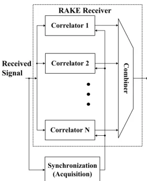
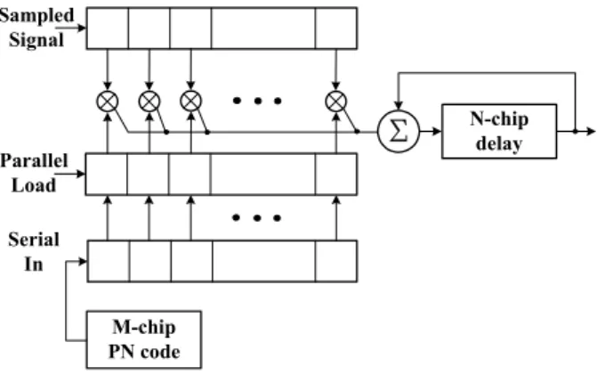
(2) performance of the spread spectrum system requires the. RAKE Receiver. receiver’s phase and frequency and its chip timing to be. Correlator 1. perfectly synchronized. The synchronization process is called code acquisition. Acquisition is based on the the mobile channel and sets the delay times of the RAKE. Received Signal. Correlator 2. fingers. The typical RAKE receiver architecture with. Combiner. received signal’s magnitude of the impulse response of. maximal ratio combining is shown in Figure 1. The matched filter correlates the received signal with local PN code to obtain the delay profile of the multipath. Correlator N. fading channel. The searcher is required to search the correlation profile. In the searcher, the threshold is set to Synchronization (Acquisition). select the peak values properly. It must set to obtain the acceptable missing probability false alarm probability. After the acquisition process is completed, the delays are. Figure 1. Simplified RAKE receiver with acquisition. passed to the tracking unit. Finally the maximum ratio combining (MRC) is employed to combine the signals from various paths.. The serial-parallel architecture is a compromise between the serial architecture and parallel architecture. It is shown in Figure 2. The serial-parallel architecture is. Acquisition Architecture In the WCDMA system, the acquisition is a. more flexible than the two other architectures. The serial-parallel architecture divides the matched filter (MF). complicated problem. In the uplink system, signals are. into several sections. The PN code coefficients are. received by base station with different propagation. loaded in groups. After each group of PN code. delays due to multipath fading channel. Code acquisition. coefficients is loaded, it provides only a section of the. process can make the phase of the locally generated PN. full correlation profile. Until each section of correlation. code within half chip duration of the received signal. The. results is summed, the full correlation profile just like. code acquisition process can find the PN offset which. that of parallel architecture is achieved.. has maximum correlation value. The matched filters with. From the viewpoint of the hardware cost, the. different window sizes are used according to the. matched filter (MF) can be reprogrammed with the next. hardware cost and acquisition time that we required. The. N-chips segment of PN code. It means that the hardware. correlators can be classified as serial or parallel. implementation complexity is lower than the parallel. architecture.. architecture..
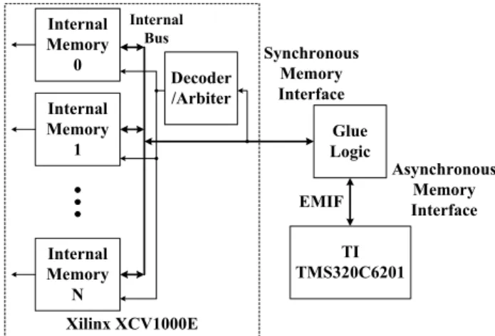
(3) multi-path. Besides, the matched filter suits to be. Sampled Signal. implemented by hardware, because it contains a lot of. Σ Parallel Load. N-chip delay. bit-shifting operation.. Matched Filter. Serial In M-chip PN code. Figure 2. The serial-parallel matched filter architecture. Implementation Feature - Task Partition between DSP and FPGA. Delay Profile Calculation Unit. Peak Search Unit. Tracking Unit. MRC. RAKE Receiver. Decoder. FPGA. DSP. Figure 3. Functional Block Diagram of the Receiver. We use the FPGA (Field Programmable Gate Arrays) and the DSP (Digital Signal Processor) to implement. - DSP/FPGA Interface. acquisition function. The principle we decide to put. We use XILINX XCV1000E FPGA and TI. which function onto the DSP or the FPGA is according to. TMS320C6201 DSP in the implementation. The capacity. the complexity of the algorithm. We put the complex. of the FPGA is million-gate. The relationship between. algorithm in the DSP and the regular computation in the. the DSP and the FPGA can consider as master-slave. We. FPGA. Besides, the capability of the DSP and the FPGA. can consider the DSP is the master and the FPGA is the. and the bus traffic of the interface between them are also. slave. The FPGA receives the primitives and parameters. under consideration. As shown in Figure 3, the functional. from the DSP. According to the primitives that the DSP. block in gray is main acquisition function. It provides. gives, the FPGA knows what the computation should be. coarse acquisition result to the tracking unit. The timing. done and uses these parameters to calculate.. resolution of the peak location from acquisition result is. The interface between the FPGA and DSP is shown. in the unit of 1/2 chip. Moreover, the tracking unit can. in Figure 4. TI DSP has provided external memory. improve the timing resolution to 1/16 chip. We can. interface, called EMIF. It is an asynchronous memory. consider it as fine adjustment of the peak location.. interface. Because the synchronous interface can avoid. The task partition between the FPAG and the DSP. some glitch errors and fits to the internal memory in the. in acquisition function can consider as the FPGA. FPGA, we use simple glue logic to transfer it to the. provides the delay profile to the DSP, and the DSP finds. synchronous memory interface. The transferred memory. the peak location. The reason why the peak searcher is. bus is connected to the internal memory bus in the FPGA.. put onto the DSP is that the peak search algorithm is. Thus DSP can access different internal memory in the. complex and needs more flexibility. It is responsible for. FPGA through EMIF. In order to avoid the conflict on. finding the peak that it is really caused by the effect of. the internal bus, the Decoder/Arbiter unit will decide.
(4) which internal memory is asserted according to the primitive that the DSP gives. Internal Memory 0 Internal Memory 1. Internal Bus. Decoder /Arbiter. .... D2 D1 D0. D. Q. D. Q. Synchronous Memory Interface Glue Logic EMIF. Internal Memory N. D. Q. Σ Asynchronous Memory Interface. TI TMS320C6201. Xilinx XCV1000E. D. CLK .... C2 C1 C0. Q. D. EN. Q. D. EN. D. Q. Q EN. D. Q. LD_EN. Figure 4. Functional Block Diagram of the DSP/FPGA. Figure 5. Example of the Circuit Design of the. Interface. Serial-to-Parallel Type Matched Filter. - Implementation Architecture of Serial-to-Parallel Type Matched Filter. In this architecture, if the tap number increase, the circuit area of the summation function will be large. In. As the description above, we decide to use. the case of WCDMA, the tap number we use is 128.. serial-to-parallel type matched filter in our system and. Therefore, there will be 128 multiple results need to be. implement it in hardware. Figure 5 shows the example of. added at one time. The traditional way is using adder tree. the circuit design of the serial-to-parallel type matched. for summation. But it takes time to process. Therefore,. filter. In this example, the tape number is 3. Therefore,. we use inverse typed serial-to-parallel matched filter.. the parameter C0,C1…Cn is parallel load to the register. The example of the inversed type serial-to-parallel. connected to the multiplier every three clock cycle. We. matched filter is shown in Figure 6.. can derive the mathematic from the summation output in the flowing:. The inversed type matched filter loads the coefficient inversely. In Figure 6, there are three load enable signals. The signal “LD_EN0” will be asserted. Cycle 1 ~ Cycle 2: in the initial state. first. After that, the signal “LD_EN1” and “LD_EN2” will. Cycle 3: D0 C0 + D1 C1 + D2 C2. be asserted in order. We can observe a dotted line with. Cycle 4: D1 C0 + D2 C1 + D3 C2. arrowhead in the mathematical form. The inversed type. Cycle 5: D2 C0 + D3 C1 + D4 C2. matched filter calculates these dotted terms first. For the. Cycle 6: D3 C3 + D4 C4 + D5 C5. example of D2, it calculates the terms “D2C0”, “D2C1”. Cycle 7: D4 C3 + D5 C4 + D6 C5. and “D2C2”. But it will add the term “D2C2” first. And. Cycle 8: D5 C3 + D6 C4 + D7 C5. the term “D2C1” will be latched for one cycle and is. Cycle 9: D6 C6 + D7 C7 + D8 C8. added in the next cycle. Therefore, it separates the.
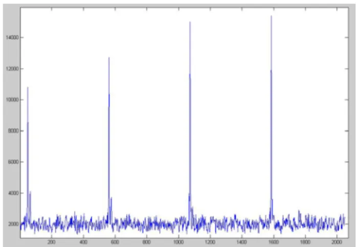
(5) summation in different cycle. It can eliminate the huge adder tree in the previous architecture. But it must carefully control the load enable signal in order to make the data be multiplied by the right coefficient. .... D2 D1 D0. D. D. Q. Q. D. Q. D. Q. Figure 7. Delay Profile calculated by the Matched. CLK. Filter D. Q. D. EN. Q. D. EN. Q EN. .... C2 C1 C0 LD_EN0. LD_EN1. LD_EN2. Area Overhead / Loading. FPGA 31 %. DSP 2.9 %. Table 1. Acquisition Function Implementation Result. Figure 6. Example of the Circuit Design of the Inversed. Conclusion. Type Serial-to-Parallel Type Matched Filter. This paper introduces the design methodology of acquisition of the WCDMA receiver. Acquisition is. - Matched Filter Implementation Result Figure 7 shows the delay profile calculated by the. important to the spread spectrum system to synchronize. matched filter. The test environment includes fading. the received signals. We use both firmware and hardware. channel which is satisfied the requirement of the 3GPP. in the implementation. The acquisition architecture. standard. We can see that the different path caused by the. would be designed for different requirements such as cell. multi-path effect can be easily distinguished.. size, fading channel and etc. Therefore, under the. Table. 1. shows. all. acquisition. function. implementation result. The first field shows the circuit. different consideration, using the hardware combined with firmware can get flexibility.. area overhead of the matched filter in the FPGA. It still has the free area for the rake receiver. The second field. References. shows the peak search algorithm computation loading to. [1]. G. J. R. Povey and P. M. Grant, “Simplified. the total DSP computing cycles. There are still a lot of. matched filter receiver designs for spread spectrum. the computing cycles can reserve for the complex. communications applications”, ELECTRONICS &. channel Codec, such like Viterbi Codec and Turbo code. COMMUNICATION ENGINEERING JOURNAL,. Codec.. pp. 59-63, April, 1993. [2]. Han-Sup Lee, Hyun-Seo Oh and Chang-Eon Kang, “Code Acquisition for DS-CDMA RAKE Receiver.
(6) in a Multipath Fading Channel”, IEEE Catalogue No. 95TH8061, pp. 215-219, 1995. [3]. Jaw W. Chung, Jin S. Kim, Young G. Jeong and Jeong S. Ha, “Implementation of Base Station Receiver for CDMA Wireless Local Loop System”, pp. 371-374, ICPWC’97.. [4]. Erik G. Strom, Scott L. Miller, Stefan Parkvall, Bjorn E. Ottersten, “DS-CDMA Synchronization in Time-Varing Fading Channels”, IEEE JOURNAL ON SELECTED AREAS IN COMMUNICATIONS, pp. 1636-1642, VOL. 14, NO. 8, OCTOBER, 1996.. [5]. Christopher. Deng. and. Charles. Chien,. “A. PN-Acquisition ASIC for Wireless CDMA System”, IEEE 2000 CUSTOM INTEGRATED CIRCUITS CONFERENCE, pp. 469-472, 2000. [6]. Yasuo Suzuki, Eisuke Kudoh and Shigeaki Ogose, “DS-CDMA RAKE Receiver with Time-Window Control Loop (TWCL) in Multipath Fading Environment”,. IEEE. TRANSATION. ON. VEHICULAR TECHNOLOGY, pp. 167-172, VOL. 49, NO. 1, JANUARY, 2000..
(7)
數據
相關文件
了⼀一個方案,用以尋找滿足 Calabi 方程的空 間,這些空間現在通稱為 Calabi-Yau 空間。.
2.1.1 The pre-primary educator must have specialised knowledge about the characteristics of child development before they can be responsive to the needs of children, set
Reading Task 6: Genre Structure and Language Features. • Now let’s look at how language features (e.g. sentence patterns) are connected to the structure
• ‘ content teachers need to support support the learning of those parts of language knowledge that students are missing and that may be preventing them mastering the
Promote project learning, mathematical modeling, and problem-based learning to strengthen the ability to integrate and apply knowledge and skills, and make. calculated
volume suppressed mass: (TeV) 2 /M P ∼ 10 −4 eV → mm range can be experimentally tested for any number of extra dimensions - Light U(1) gauge bosons: no derivative couplings. =>
Courtesy: Ned Wright’s Cosmology Page Burles, Nolette & Turner, 1999?. Total Mass Density
• We shall prove exponential lower bounds for NP-complete problems using monotone circuits. – Monotone circuits are circuits without
