SIMULATION OF SEMICONDUCTOR PROCESSES AND DEVICES Vol. 12 233 Edited by T. Crasser and S. Selberherr - September 2007
Numerical Simulation of Field Emission in the Surface
Conduction Electron-Emitter Display
Hsiang-Yu Lo, Yiming Li, Hsueh-Yung Chao, Chih-Hao Tsai*, Fu-Ming Pan*, Mei-Chao Chiang**, Ting-Chen Kuo**, and Chi-Neng Mo**
Department of Communication Engineering; *Department of Materials Science and Engineering, National Chiao Tung University, Hsinchu 300, Taiwan
hylo.cm95g@nctu.edu.tw; ymli@faculty.nctu.edu.tw; hychao@cm.nctu.edu.tw;
italno0613@yahoo.com.tw; fmpan@faculty.nctu.edu.tw
Chunghwa Picture Tubes, Ltd., Taoyuan, Taiwan {jiangm|kuoku|mocn}@mail.cptt.com.tw
Abstract
We employ a three-dimensional (3D) particle-in-cell method coupling with finite-difference time domain scheme to simulate the electron emission in surface conduction electron-emitter displays (SEDs). This computational technique includes the space charge effects automatically. We thus explore the conducting mechanism, the emission efficiency, and the current density distribution on the anode plate with one field emission emitter.
1 Introduction
Surface conduction electron-emitter display (SED) is a new type of flat panel display based on surface conducfion electron-emitters (SCEs) [1-3]. The potenfialifies of SCEs as field emission sources are superior to conventional cathodes in many respects. These SEDs possess high luminance, good color, as well as low power consumption. However, the emission efficiency is determined by the shape and material of SCE. Studies on SCE have not been clearly understood yet. Even if the multiple scattering model of the electron emission mechanism of the SCE has been proposed [4], 3D Maxwell-particle-in-cell simulation [5] has not been considered for the electron emission of SED yet.
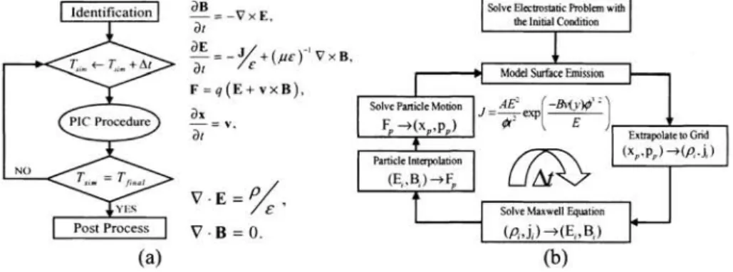
2 Simulation Technique
The schematic of the emitter structure and related experiment setup is shown in Fig 1(a). The emitter has a coplanar structure with a palladium nanogap which is fabricated by the focused ion beam technology, and the width is approximately 90 nm. Because the dimension of nanogap is much smaller than that of device, a region requires rapid variation in the cell. Therefore, the mesh generation by the Pade function is recommend and the creation of grids near the nanogap region is plotted in Fig. 1(b). We can find that it results in a Pade function-spaced grid over the region. The voltage is 60 V applied to a conductive film including Pd via a Pt electrode. A
234 SIMULATION OF SEMICONDUCTOR PROCESSES AND DEVICES Vol. 12 Edited by T. Crasser and S. Selberherr - September 2007
program has been developed to simulate the emission efficiency and the electron mechanisms of different emission structure. The 3D finite-difference time domain code for self-consistent simulation of the electromagnetic fields and charged particles are performed in our simulation. The computational scheme and the related equations based on physical basis are shown in Fig. 2.
Figure 1: (a) A schematic plot of the SED structure and the cross section of the
surface conduction electron-emitter on the x-z plane, (b) Mesh generation by using the Fade function grids near the nanogap.
5B ^ ^ = - V x E ,
dt
Solve Electrostatic Problem with the Initial Condition
aE = - J /
F = q(E + \xB),
— = dt ' " ' '
V B = 0.
Solve Particle Motion
Particle Interpolation
(E.B,)-^F^
J =—;-exp •
^S5>
Solve Maxwell Equation
(flJ,)^(E,.B,)
(b)
•W Model Surface Emission i—
Extrapolate to Grid
Figure 2: (a) The computational scheme and the corresponding equations for the
electron emission simulation, (b) The flowchart of FIC procedure.
3 Results and Discussion
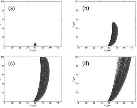
According to our calibrated model [6], high accuracy results could be obtained in this work. Figure 3(a) shows the contour plot of electric fields with the anode voltage (Va) is 3000 V, and the gate voltage (Vg) is 60 V. The fields are higher around the emitter apex and the electrons here are accelerated to energies sufficient to be tunneled fi'om the metal into vacuum. The 3D electron trajectory is shown in Fig. 3(b). The electron beam emits toward the driver electrode and goes upwards to the anode. The cross sections of Fig. 3(b) on the x-z plane with different simulation time are shown in Fig. 4. This is clearer to know the electron-emission mechanism. When the electrons
SIMULATION OF SEMICONDUCTOR PROCESSES AND DEVICES Vol. 12 Edited by T. Crasser and S. Selberherr - September 2007
235
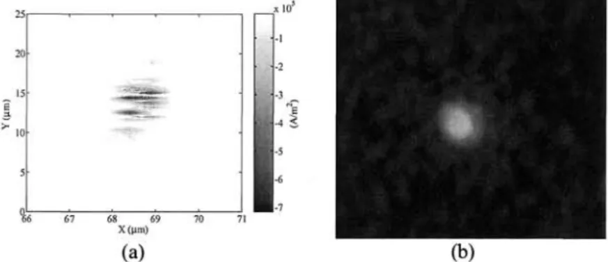
emitted to the anode, Fig. 5(a) shows the current density distribution on the anode plate. From this result, the current can be evaluated by integrating the current density to the area. Its value is about 5 \xA which is large enough to let the phosphor luminance. The light spot which is produced on the phosphor plate of spacer of 500 |um apart from the emitter is shown in Fig. 5(b) when Va = 3 kV and Vg = 60 V. The achieved performance is coincided with the suppositions in [1-3].
i^mSMi
37.4 37.45 37.5 37.55 37.6 X (mil) (a) X 10 1 15 ? 1-9 ••10 Z ijtm)Figure 3: (a) The contour plot of electric fields in nanogap of 90 nm wide, (b) The
3D electron trajectories of the SED structure. The gate voltage is 60 V and anode voltage is 3000 V, respectively.
(a)
iO 20 .10 10 50 60 70(b)
iJ
10 20 30 -10 30 ^0 70 >:(,im)(c)
10 20 30 10 50 ^0Figure 4: The electron beam ejected fi'om the SCE on the x-z plane with various time.
236 SIMULATION OF SEMICONDUCTOR PROCESSES AND DEVICES Vol. 12 Edited by T. Grasser and S. Selberherr - September 2007
Figure 5: (a) The simulated current density distribution on the anode plate, (b) The
image of a light spot was produced on the phosphor plate.
4 Conclusions
We have developed a 3D simulation scheme for the electron emission by using a surface conduction electron emitter. The results including the electron-emission mechanism, current density distribution on the anode plate, and high emission efficiency have been calculated and discussed. They promise the advantages of the SED for TV applications.
Acknowledgements
This work was supported in part by Taiwan National Science Council (NSC) under Contract NSC-95-2221-E-009-336, Contract NSC-95-2220-E-009-030, Contract NSC-95-2752-E-009-003-PAE, by MoE ATU Program, Taiwan, under a 2006-2007 grant, and by the Chunghwa Picture Tubes under a 2006-2007 grant.
References
[1] K. Birdsall and A. B. Langdon, Plasma Physics via Computer Simulation, McGraw-Hill, New York (1985).
[2] K. Sakai, I. Nomura, E. Yamaguchi, M. Yamanobe, S. Ikeda, T. Hara, K. Hatanaka, Y. Osada, H. Yamamoto, T. Nakagiri, "Flat-Panel Displays Based on Surface-Conduction Electron Emitters," Proc. Euro Display '96, 18.3, 569 (1996).
[3] Asai, M. Okuda, S. Matsutani, K. Shinjo, N. Nakamura, K. Hatanaka, Y. Osada, T. Nakagiri, "Multiple-Scattering Model of Surface-Conduction Electron Emitters," SID '97 DIGEST 10.4, 127 (1997).
[4] E. Yamaguchi, K. Sakai, I. Nomura, T. Ono, M. Yamanobe, N. Abe, T. Hara, K. Hatanaka, Y.Osada, H. Yamamoto, and T. Nakagiri, "A 10-in. Surface-Conduction Electron-Emitter Display," SID '97 DIGEST, 6.2, 52 (1997).
[5] M. Okuda, S. Matsutani, A. Asai, A. Yamano, K. Hatanaka, T. Hara, T. Nakagiri, "Electron Trajectory Analysis of Surface Conduction Electron Emitter Displays (SEDs)," SID '98 DIGEST, 14.1, 185 (1998).
[6] H.-Y. Lo, C.-H. Tsai, H.-Y. Chao, Y. Li, F.-M. Pan, T.-C. Kuo, M. Liu, and C.-N. Mo, "Three-Dimensional Simulation of Novel Surface Conduction Electron Emitters," to be presented in Int. SID Symp. Seminar and Exhibition, CA, U.S.A., May 20-25, 2007.