國
國
國
國 立
立
立
立 交
交
交
交 通
通
通
通 大
大
大
大 學
學
學
學
電子工程學系
電子工程學系
電子工程學系
電子工程學系 電子研究所碩士班
電子研究所碩士班
電子研究所碩士班
電子研究所碩士班
碩
碩
碩
碩 士
士
士 論
士
論
論 文
論
文
文
文
二位元
二位元
二位元
二位元分離式閘極
分離式閘極
分離式閘極
分離式閘極氮化矽快閃式記憶體
氮化矽快閃式記憶體
氮化矽快閃式記憶體
氮化矽快閃式記憶體之
之
之
之
先進操作方法探討
先進操作方法探討
先進操作方法探討
先進操作方法探討
The Investigation of a Novel Operating Method for
Two-Bit Split Gate SONOS Flash Memory
研 究 生 :周承翰
指導教授 :莊紹勳 博士
二位元分離式閘極氮化矽快閃式記憶體之先進
二位元分離式閘極氮化矽快閃式記憶體之先進
二位元分離式閘極氮化矽快閃式記憶體之先進
二位元分離式閘極氮化矽快閃式記憶體之先進
操作方法探討
操作方法探討
操作方法探討
操作方法探討
The Investigation of a Novel Operating Method for
Two-Bit Split Gate SONOS Flash Memory
研 究 生 : 周承翰 Student : Chen-Han Chou
指導教授 : 莊紹勳 博士 Advisor : Dr. Steve S. Chung
國立交通大學
電子工程學系 電子研究所碩士班
碩士論文
A Thesis
Submitted to Department of Electronics Engineering & Institute
of Electronics College of Electrical and Computer Engineering
National Chiao Tung University
in Partial Fulfillment of the Requirements
for the Degree of Master of Science
in Electronics Engineering
July 2011
Hsinchu, Taiwan, Republic of China.
二位元分離式閘極氮化矽快閃式記憶體之先進
二位元分離式閘極氮化矽快閃式記憶體之先進
二位元分離式閘極氮化矽快閃式記憶體之先進
二位元分離式閘極氮化矽快閃式記憶體之先進
操作方法探討
操作方法探討
操作方法探討
操作方法探討
學生:周承翰 指導教授:莊紹勳博士
國立交通大學電子工程學系電子研究所碩士班
摘要
摘要
摘要
摘要
此論文將提出在二位元分離式閘極氧化矽快閃式記憶體上先進的操作方 法。在許多種不同的分離式閘極結構,源極注入(SSI)最常被使用在寫入以及帶 對帶電洞入射(BTBHHI)則是用於抹除。有鑒於常見入射電荷的操作方法下,電子 與電洞在底層氧化層的反應將會導致些可靠度上的議題,還有,底層氧化層的應 力感應漏電流(SILC)現象已經在快閃記憶體中被視為主要的可靠度議題。在不同 的抹除方法中,熱電洞入射引起的氧化層退化已被發現是蠻嚴重的情形,論文裡 我們將提出新的抹除操作模式來抑制抹除對氧化層的破壞。 首先關於新的操作模式的電壓時間關係使用了多循環脈衝系列來加強寫入 /抹除的效率,在寫入方法中-順向偏壓促進電子入射(FBEI)是由順向偏壓促進電 子入射以及新的抹除方法-順向偏壓促進熱電洞入射(FBHHI)則是藉由合適的順 向偏壓來產生電洞,FBEI可以達成低電壓以及高速度的操作目的,而抹除時使用 FBHHI可以比BTBHHI用更少的時間產生更多的電洞。從實驗結果可得知新的操作 模式比常見的操作更可靠。 最後,我們利用特殊的分離式閘極結構來分析不同的寫入方式造成的電荷 分佈以及第二位元的影響(SBE),並且在二位元的操作上使用多循環脈衝系列的 操作方式,我們可以得到相對於常見的操作較好的性能及可靠性表現。The Investigation of a Novel Operating Method for
Two-Bit Split Gate SONOS Flash Memory
Student:Chen-Han Chou Advisor:Dr. Steve S. Chun
g
Department of Electronics Engineering & Institute of Electronics
National Chiao Tung University
ABSTRACT
In this thesis, a novel operating scheme has been proposed for 2-bit/cell split
gate SONOS. For a certain design of split gate structure, source-side injection (SSI) is
usually used for programming and band-to-band hot hole injection (BTBHHI) is used
for erase. By using the conventional operating method of charge injection, the
interaction between the generated electron and hole pairs could cause the reliability
issue for bottom oxide. Stress induced leakage current (SILC) at the bottom oxide has
been discussed as a major reliability issue in flash memory. Among different erase
method, hot hole injection induced oxide degradation has been found to be most
serious condition. In thesis, we propose the new operating scheme to suppress the
oxide damage during erase.
First, the new timing diagram for novel operating scheme used the multi-cycle
(FBHHI), achieved by suitable forward-bias assisted hole generation were proposed.
A lower voltage operation and high speed operation can then be implemented in FBEI
program. For the erase, FBHHI can supply more holes and less time than BTBHHI in
the same operation condition. The results showed that the new operation schemes are
more reliable than conventional operation.
Finally, we used the specific split gate structure to analyze the charge profiling
of various program methods and second bit effect (SBE). And then, a 2 bit/cell
operation for split gate SONOS by using multi-cycle pulse series, in which better
performance and reliability can be achieved in comparison to conventional operation
Acknowledgements
碩士生活的兩年是短暫卻又充實的,交織著酸甜苦辣的實驗室日子。首先要 感謝我的指導教授莊紹勳老師,莊老師不僅在研究上給予許多指導建議,教我應 具有的研究精神跟態度,並在課業與生活上,也有許多的關懷,在此深表我對老 師的感謝。 感謝何永涵學長在實驗研究上的細心教導,並且給予我許多的建議跟指導, 感謝曾元宏、鄭世嵩、程政穎學長,給予學業跟實驗上的解答跟協助。還有感謝 這兩年研究生涯的夥伴嘉偉、志宇,在日常的生活中,因為有你們,讓實驗研究 生活變得更加有趣,相信數年後再聚,定倍感溫馨。也感謝汪老師研究群的邱榮 標學長,雖然在不同的研究群中,但實驗室有你們,使得乏味的實驗室生活更多 采多姿。此外,也感謝學弟蔡政達、黃英傑、蔡漢旻、蔡侑璉,感謝你們對實驗 室的付出,使得學長們能專心於實驗研究上,真心的祝福你們明年可以順利畢 業。總歸一句,感謝所有的夥伴,因為有你們,使我這兩年研究生活豐富且精彩, 即使艱辛,仍充滿歡笑。 另外,在此也要感謝聯華電子在測試元件和儀器上的協助,讓本研究才得以 順利完成。 最後要感謝我家人們,你們是我最大的精神支柱,有了你們的支持和鼓勵, 讓我能堅持到現在。 謹將這份榮耀獻給培育我多年的父母親。Contents
Chinese Abstract --- i
English Abstract --- ii
Acknowledgements --- iv
Content --- v
Table Caption --- vii
Figure Captions --- viii
Chapter 1 Introduction……….……….… 1
1.1 The Motivation of this Work………
…..
………….
11.2 Organization of the Thesis……….. 2
Chapter 2 Device Fabrication and Equipment Setup……...….. 4
2.1 Introduction……….………... 4
2.2 Device Fabrication………..……….………... 4
2.3 Experimental Setup…………..………... 5
2.4 Programming and Erasing Setup……… 6
2.5 Charge Pumping Measurement Technique Setup………...……… 7
Chapter 3 A Novel Operating Scheme and Properties of Split-Gate SONOS
…………18
3.1 Introduction……….…... 18
3.2 Basic Mechanism and Optimized Bias Condition of Novel Operation Scheme………... 18
3.2.1 The Operating Mechanisms of FBEI and FBHHI………...………... 18
3.2.2 Optimized Vhigh and Vlow of FBEI program..………...………... 19
3.2.3 Optimized VD,low of FBHHI Erase……… 20
3.2.4 Program/Erase Transient for Different Modes of Operation……… 20
3.3 Reliability for Non-Cycled Split-Gate SONOS……….…….…….……….. 20
3.3.1 Operating Mode of P-N+ Diode………...………. 21
3.3.2 The Comparison with FBHHI and BTBHHI Erase……… 21
Chapter 4
The Monitoring of Stored Charges and Oxide Traps in a Planar
SONOS ……….
34
4.1 Introduction……… 34
4.2 Principle of Charge Profile by Charge Pumping Method………... 34
4.2.1 Principle of Charge Pumping Method…………...………..…………... 34
4.2.2 Fixed Base Charge Pumping Method……….………..……… 36
4.2.3 Fixed Top Charge Pumping Method…...………..……… 36
4.3 The Monitoring of Stored Charges for a Cycled Cell………... 37
4.3.1 The Correlation Between Stored Charges and ICP in FVb CP Method……… 4.3.2 Derivation of the Area Parameter……… 37 38 4.3.3 The Correlation Between Stored Charges and Area Parameter……… 40
4.4 Experimental Results and Discussion………... 40
4.4.1 The Basic Operation Conditions of Different Operating Schemes……… 40
4.4.2 The Experiment Results of FVb CP method 41
Chapter 5 Reliability Analysis of Two Bit per Cell Operation Split-Gate SONOS
53
5.1 Introduction……….... 535.2 The Basic Electrical Characteristic in Split-Gate SONOS………. 54
5.3 Basic Characteristics on the Programming Cells………. 54
5.3.1 Results on the One-Bit Programming Cells……… 55
5.3.2 Applications to Two-Bit Programming Cells………. 56
Chapter 6 Summary and Conclusion………...… 72
Table Caption
Figure Captions
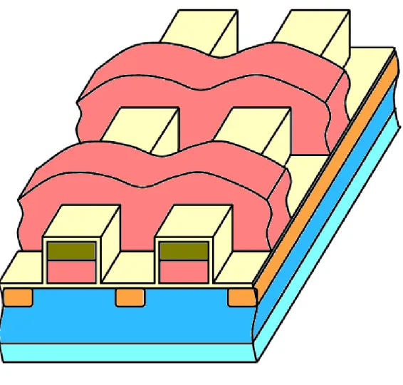
Fig. 2.1 The schematic diagram illustrating of forming the dual-bit split-gate SONOS.
Fig. 2.2 (a) The SEM image and (b) the simulation structure of the dual-bit split-gate SONOS.
Fig. 2.3 The experimental setup of the current-voltage and the transient characteristics measurement. An automatic controlled characterization system is setup based on the PC controlled instrument environment.
Fig. 2.4 (a) The operation scheme and (b) timing diagram for CHEI program.
Fig. 2.5 (a) The operation scheme and (b) timing diagram for BTBHHI erase.
Fig. 2.6 (a) The operation scheme and (b) timing diagram for FBEI program
Fig. 2.7 (a) The operation scheme and (b) timing diagram for FBHHI erase.
Fig. 2.8 The operation scheme for charge pumping with (a) fixed base pulse measurement and (b) fixed top sketch.
Chapter 3
Fig. 3.1 (a)The conventional unit-cycle pulse series for CHEI or BTBHHI. (b)The multi-cycle pulse series for FBEI or FBHHI .
Fig. 3.2 The operation scheme and timing diagram for (a) FBEI program and (b) FBHHI erase. The FBEI pulse series were combined with the same pulse width, but the FBHHI series used a varying pulse width.
Fig. 3.3 The characteristics of FBEI as a function of VD,low.
Fig. 3.4 (a) The characteristics of FBEI as a function of VD,high .
(b) The characteristics of FBEI as a function of VG.
Fig. 3.5 The characteristics of FBHHI as a function of VD,low.
Fig. 3.6 The programming transient of SSI and FBEI programs for split-gate SONOS with multi-level cell application.
application.
Fig. 3.8 Two different modes of measurement for split-gate SONOS.
Fig. 3.9 By using multi-cycle pulse series, it only used a half of operating time to be stressed at high voltage and remaining time be stressed at low voltage.
Fig. 3.10The mechanism of multi-cycle pulse series operation. The generation of carrier is far away from the channel and reduces the oxide degradation.
Fig. 3.11 The value of leakage current and threshold voltage at VD=-2V, even if it is until a thousand
seconds.
Chapter 4
Fig. 4.1 (a) The VT profile in a programmed nitride storage memory cell.
(b) Illustration of Icp curves versus Vh before and after the programming.
Fig. 4.2 (a) The VT profile in a programmed nitride storage memory cell.
(b) Illustration of Icp curves versus Vb before and after programming.
Fig. 4.3 The schematic FVb charge-pumping current curves related to the trapping charges and interface traps for a planar SONOS.
Fig. 4.4 The difference of ICP,d curves for fresh state and one time program state in a planar SONOS.
The area Ao in the shade region represents the total stored electrons in the nitride after the
first time programming.
Fig. 4.5 The endurance for planar SONOS with different operation combinations.
Fig. 4.6 The ICP,d versus VHIGH for a planar SONOS with (a) CHEI/BTBHHI cycle and (b)
FBEI/BTBHHI cycle during different cycling times by using fix base charge-pumping method.
Fig. 4.7 The ICP,d versus VHIGH for a planar SONOS with (a) CHEI/FBHHI cycle and (b)
FBEI/FBHHI cycle during different cycling times by using fix base charge-pumping method.
Fig. 4.8 The ∆A/Ao versus P/E cycle with four operating combinations
Fig. 4.9 The ∆ICP,max/ICPo,max versus P/E cycle with four operating combinations.
Chapter 5
Fig. 5.1 The schematic structure of the split-gate SONOS.
Fig. 5.2 The drain current versus gate voltage under forward read and reverse read when the VCG
was biased at 0.9V in a split-gate SONOS.
Fig. 5.3 (a) The threshold voltage shift with varying VCG.
(b) The ID-VG curves with different VCG conditions.
Fig. 5.4 The negative channel potential along lateral location with different VCG= 0.6V , 0.7V and
0.8V conditions at CC-Vth= 56nA.
Fig. 5.5 (a) The threshold voltage shift with varying VD.
(b) The negative channel potential along lateral location with different VD =0.2 ~ 1.8V
conditions
Fig. 5.6 The diagram of the forward read and reverse read modes.
Fig. 5.7 The window versus Vth shift of bit-1 for split-gate SONOS with LWG= 0.1 and 0.13 um.
Fig. 5.8 The window for various read voltage with different ∆Vth (bit-1), using (a) SSI program and (b) FBEI program. The star symbol indicated the saturation point.
Fig. 5.9 The window for various VCG with different ∆Vth of bit-1 by (a) SSI program and (b) FBEI
program.
Fig. 5.10The operating mechanism of SSI and FBEI programs.
Fig. 5.11The programming speed for the first bit and second bit by FBEI and SSI programs.
Fig. 5.12Endurance characteristics of two-bit per cell application, using SSI program and FBHHI erase.
Fig. 5.14Retention behaviors after 10k P/E of Bit-1 at Vth high and Vth low states with FBEI/FBHHI
Chapter 1
Introduction
1.1
The Motivation of This Work
In charge-trapping devices, such as SONOS memory, 2-bit per cell operation
becomes the basic requirement of a flash memory, which is also a popular solution for the cell scaling. So far, many unique gate structure cells [1][2] have been proposed to
improve the non-volatile memory (NVM) performance based on the operation scheme approach. For the specific split gate structure [3], in most cases, the cell is
programmed by channel hot electron (CHE) or source-side injection (SSI) [1], while erase is achieved by band-to-band hot hole injection (BTBHHI) [4]. Based on a
forward-bias assisted electron injection (FBEI) scheme that our group developed in [5], where a low voltage, high speed program, and excellent data retention could be
achieved. From various erase mechanisms, a major reliability issue in flash memory is the hot hole injection induced oxide degradation [6]. The positive charge-assisted
tunneling (PACT) was found to be a dominant stress induced leakage current (SILC) mechanism in HH stress [7]. An efficient erase method forward-bias assisted hot hole
injection (FBHHI) was then developed to improve the BTBHHI erase scheme by using the suitable forward bias in drain/substrate p-n+ diode. As a consequence, the
experimental result was demonstrated that FBHHI erase can suppress the oxide damage.
charge profiling of the dielectric layer with only program or erase condition.
Nevertheless, it becomes more inaccurate after P/E cycles. In a fixed voltage base (FVb) charge pumping method, by further improving the method in [10], the
hole-electron misalignment and oxide degradation of operation after P/E cycling can be further understood. Therefore, we can easily distinguish the residue charge of the
dielectric layer under different program/erase combinations.
In this thesis, we used the specific split gate structure to study the charge distribution with various program methods and the second bit effect (SBE). And then,
the new operation schemes for program/erase which are applicable for 2 bit/cell operation has been discussed. The degradation of bottom oxide can be suppressed in
comparison to conventional operation scheme by using the multi-cycle pulse approach. Finally, we will draw a conclusion of the thesis.
1.2
Organization of the Thesis
The organization of this thesis consists of six chapters. After a brief introduction in Chapter 1, we will introduce the experimental devices and experimental setup in Chapter 2, which includes the operating schemes, program and erase, and the measuring method of charge pumping. In Chapter 3, we will introduce the mechanisms of FBEI and FBHHI and we will compare the performance and reliability with different program/erase schemes. In Chapter 4, we will explain the phenomenon of charge-pumping method in planar SONOS devices, which led to a development of a new monitor, defined as A. As a consequence, we will study the different operation combinations with this new parameter area A. In Chapter 5, we will focus on the
operation in different pulse series type will be discussed. Finally, the summary will be presented in Chapter 6.
Chapter 2
Device Fabrication and Equipment Setup
2.1 Introduction
This chapter is divided into four sections. First of all, both split-gate SONOS and the conventional SONOS cells used in this study will be described. Second, the
instruments setup and the experimental techniques to accurately control these instruments are illustrated. Third, we will discuss the new programming and erasing
schemes of these cells. Finally, charge pumping measurement technique setup used in this study will be demonstrated.
2.2 Device Fabrication
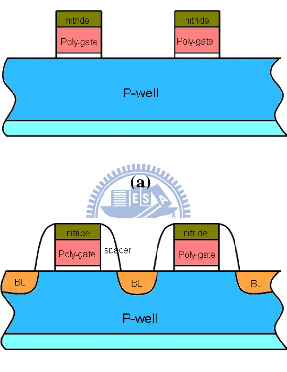
Figure 2.1 is the schematic diagram illustrating the fabrication of split-gate
SONOS. As shown in Fig. 2.1(a), a substrate is provided, and a P well is formed in the substrate. Then, a plurality of control gate structure is formed on the P well. Each
control-gate structure from bottom to top includes a gate insulating layer, a control gate oxide (65Å), and a cap nitride layer. As shown in Fig. 2.1(b), a silicon oxide
layer (not shown), a nitride layer (not shown) is deposited on the substrate and control gate structure, and an etching back process is then performed to form a plurality of
sacrificial spacers alongside each control gate structure. Meanwhile, a plurality of opening is formed between any two adjacent sacrificial spacers to expose the P well.
Afterward, an implantation process is performed via each opening to form a plurality of N doped regions, serving as buried bit line, in the P well. As shown in Fig. 2.1(c),
composite dielectric layer is formed on the P well, the control-gate structure, and the
N doped regions. In this embodiment, the composite dielectric layer is an ONO tri-layer dielectric including a bottom oxide layer (60Å), a nitride layer (90Å), and a
top oxide layer (90Å). As shown in Fig. 2.1(d), a conductive layer is entirely deposited on the composite dielectric layer, and a photolithography and etching
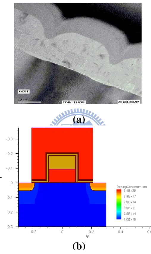
process is performed to define a plurality of parallel word line, which are perpendicular to the control-gate structure, as shown in Fig. 2.1(e) [11]. The SEM
image and the 2D-TCAD simulation structure of dual-bit split-gate SONOS are shown in Fig. 2.2 (a) and Fig. 2.2 (b). The gate width is 0.2um, and the channel length
is 0.18um under control-gate and three different word gate length (LWG) splits
(0.13um, 0.12um, 0.10um) under the word-gate.
The conventional SONOS cell used in this study is first grown by thermal
oxidation with thicknesses of 50 Å. Next, a layer of 60 Å LPCVD nitride film is grown. Finally, the LPCVD blocking oxide is grown with thickness of 50 Å.
(W/L=0.7/0.26 um)
2.3 Equipment Setup
The experimental setup for the I-V and transient characteristics measurement of SONOS is illustrated in Fig. 2.3. Based on the PC controlled instrument environment
via HP-IB (GP-IB, IEEE-488 Standard) interface, the complicated and long-term characterization procedures during analyzing the intrinsic and degradation behaviors
station provides an adequate capability for measuring the device I-V characteristics
and executing the SONOS cell program/erase operation.
Source-monitor units (SMU) and provided the high current resolution to 10-15A range facilitates the gate current measurement, sub-threshold characteristics extraction,
and the saturation drain current measurement. The HP E5250A equipped with a 10-input (6 SMU ports and 4 AUX ports) × 12-output switching matrix, switches the
signals from the HP 4156C and the HP 8110A to device under test (DUT) in probe station, automatically. In addition, the HT-Basic are used as the program languages to
achieve the personal computer (PC) control of these measurement instruments.
2.4 Programming and Erasing Setup
The general programming and erasing schemes for the conventional SONOS are Channel Hot Electron Injection (CHEI) and Band-to-Band Tunneling Hot Hole
Injection (BBTHHI). For CHEI programming, source and substrate are grounded, while gate and drain are connected to the pulse generator as shown in Fig. 2.4 (a). The
pulse timing diagram for both gate and drain are shown in Fig.2.4 (b). For BBTHHI erasing, substrate is grounded, and gate and drain are connected to the pulse generator
just like CHEI, but keeps bulk floating this time as shown in Fig. 2.5 (a). The pulse timing diagram for both gate and drain are shown in Fig.2.5 (b). The novel
programming scheme and erasing scheme for the split gate SONOS are Forward Bias assisted Electron Injection (FBEI) and Forward Bias assisted Hot Hole Injection
(FBHHI). For FBEI programming, source is floating and substrate is ground, while gate and drain are connected to the pulse generator as shown in Fig. 2.6 (a) The pulse
is floating and gate is grounded, while gate and substrate are connected to the pulse
generator as shown in Fig. 2.7 (a). The pulse timing diagram for both gate and drain are shown in Fig.2.7 (b). The operation mechanism and relevant measurement of
FBHHI will be discussed after this chapter.
Dual-bit split-gate SONOS operates as conventional does, but adding a control-gate bias in the middle of the cell. The control-gate keeps a small constant
bias for programming, while floating for erasing. And the other terminals are just the same as conventional operation.
2.5 Charge Pumping Measurement Technique Setup
The charge pumping measurement technique setup is shown in Fig. 2.6, which
we called fixed based charge pumping, but with minor difference from the traditional one. The pulse generator is connected to the gate, and with the substrate and drain
connecting to the HP4156C, while source is kept floating. Fig. 2.8 (a) shows the pulse series type sending out from the pulse generator used by this setup. By using this
setup, we can measure the charge pumping current from drain. If one wants to measure the charge pumping from drain (/source), we should connect the HP4156C
with them and open the source (/drain) to get the information of the charge pumping current. The second scheme for charge pumping measurement technique setup is
shown in Fig. 2.8 once again. However, the pulse series type is different this time. As shown in Fig. 2.8 (b), we used likely the traditional fixed top charge pumping pulse
(a)
(b)
Fig. 2.1 The schematic diagram illustrating of forming the dual-bit split-gate SONOS.
(c)
(d)
Fig. 2.1 The schematic diagram illustrating of forming the dual-bit split-gate SONOS.
(e)
Fig. 2.1 The schematic diagram illustrating of forming the dual-bit split-gate SONOS.
(a)
(b)
Fig. 2.2 (a) The SEM image and (b) the simulation structure of the dual-bit split-gate SONOS.
Fig. 2.3 The experimental setup of the current-voltage and the transient characteristics measurement. An automatic controlled characterization system is setup based on the PC controlled instrument environment.
01000 Probe Station Personal Computer HP 81110A Pulse Generator Parameter Analyzer HP 4156C Switch Matrix HP 5250 A
(a)
(b)
Fig. 2.4 (a) The operation scheme and (b) timing diagram for CHEI program.
S D VG: pulse VD: pulse BOX TOX Nitride P-sub Poly-Gate
(a)
(b)
Fig. 2.5 (a) The operation scheme and (b) timing diagram for BTBHHI erase.
S D VG: pulse VD: pulse BOX TOX Nitride VS: floating P-sub Poly-Gate
(a)
(b)
Fig. 2.6 (a) The operation scheme and (b) timing diagram for FBEI program.
S D VG: pulse VD: pulse BOX TOX Nitride VS: floating P-sub Poly-Gate
(a)
(b)
Fig. 2.7 (a) The operation scheme and (b) timing diagram for FBHHI erase.
S D VG: pulse VD: pulse BOX TOX Nitride VS: floating P-sub Poly-Gate
(a)
(b)
Fig. 2.8 The operation scheme for charge pumping with (a) fixed base pulse series measurement and (b) fixed top sketch.
S D VG: pulse VD: Icp,d BOX TOX Nitride VS: floating P-sub Poly-Gate
(or Icp,s) (or floating)
S D VG: pulse VD: Icp,d BOX TOX Nitride VS: floating P-sub Poly-Gate
Chapter 3
A Novel Operating Scheme and Properties of
Split-Gate SONOS
3.1 Introduction
In chapter 3, we will propose a new mode of pulse operation to compete with
the conventional operation scheme in split-gate SONOS. A novel operation concept used the multi-cycle pulse series and suitable forward-bias to enhance the efficiency
of program/erase. Finally, several cell reliability issues by using the new operation scheme, such as forward-bias current disturbance, transient, endurance, and stress
induced leakage current will be discuss in this chapter.
3.2 Basic Mechanism and Optimized Bias Condition of the
Novel Operation Scheme
3.2.1 The Operating Mechanisms of FBEI and FBHHI
First, two modes of pulse operation are shown in Fig. 3.1, in which Fig. 3.1(a)
shows the typical unit-pulse for conventional operation scheme, e.g., SSI or BTBHHI etc., and Fig. 3.1(b) shows a multi-cycle pulse series for new operation scheme, e.g.,
FBEI or FBHHI. In Fig. 3.1(b), the drain voltage was negative in 0 state, in which p-n+ diode was forward-biased to generate lots of carriers for increasing operating
floating, during emitting phase T1, the drain/bulk was forward biased and electrons
were injected into the bulk. Subsequently, at T2, the junction was reverse biased which
will cause the previously injected electrons in the bulk to be accelerated across the
depletion region and injected into the gate oxide.
FBHHI erase is shown in Fig. 3.2(b), substrate was grounded, while gate and drain bias used multi-cycle pulse series. Erase speed decays, for the pulse structure in
Fig. 3.2(a), due to the trapping holes at the bottom oxide which leads to a decreasing FN field. The different emitting time T2 can compensate the degradation of erase
speed. During T1, a large number of holes were injected into the drain side. Above all,
we will get higher density of holes to enhance erase speed and keep the better quality
of bottom oxide than that of BTBHHI erase (will be discussed in the next chapter).
3.2.2 Optimized V
highand V
lowof FBEI Program
Figure 3.3 shows the characteristics of FBEI as a function of VD,low for a
VG=6.5V. We found that the ∆Vth have a peak value at VD,low= -2V and it will not be
increased even if it is less than -2V. A suitable forward-bias is used to generate programming electron rather than to accelerate electron speed. Fig. 3.4(a) shows that
a VD,high of over 5.5V is required for optimized injection voltage, due to the fact that
hot electrons must surmount the ∆Ec of the Si/SiO2 interface (~3.1eV). The threshold
voltage shift decreases when the voltage is over 5.5V, since the lateral electric field is
larger than the vertical electric field. In Fig. 3.4(b), the ∆Vth was increased with raising VG. By using these optimized voltages, we can achieve an efficient operation
3.2.3 Optimized V
D,lowof FBHHI Erase
Figure 3.5 shows the characteristics of FBHHI as a function of VD,low. The shift
in the threshold voltage was saturated against increases in the forward-bias. Because the holes accumulated in the n+ drain will be recombined with electrons. Therefore, it
is no useful by adding too large forward-bias at p-n+ diode and larger forward current will cause lots of reliability issues [12].
3.2.4 Program/Erase Transient for Different Modes of Operation
The programming speed of SSI and FBEI are compared in Fig. 3.6, which
reveals that the new scheme, FBEI, achieving a faster programming speed and low voltage. In Fig. 3.7, it shows the most noticeable result in that the erase speed was
greatly increased when Vhigh of drain voltage are 4V and 5V, respectively, and the low
voltage of VD was set at -2V. We understood that the larger Vhigh of drain voltage
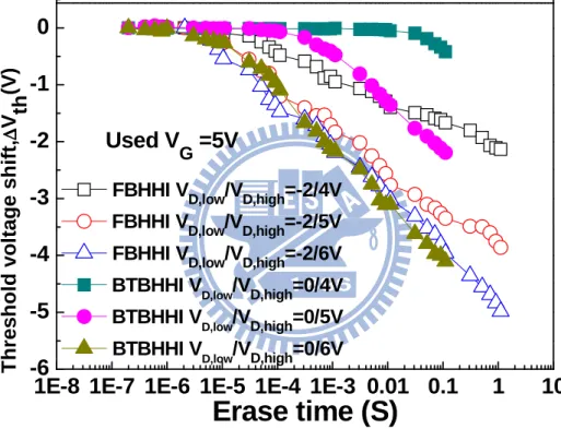
made more serious band bending to generate lots of band-to-band tunneling hot holes [4]. From the result of erase transient, we can estimate that the number of erasing hole
by using forward-bias -2V at p-n+ diode is larger than that by using reverse-bias drain voltage 4V and 5V and are comparable when the drain diode is reverse-biased at 6V.
Generally, it induces lots of hot holes by using a slight forward-bias, even if the Vhigh
is too low. We know the large reverse-bias will stress the PN junction and a huge
current also made the problem of circuit design and junction breakdown [13]. In the next section, we will discuss the reliability issue of FBHHI and BTBHHI erase.
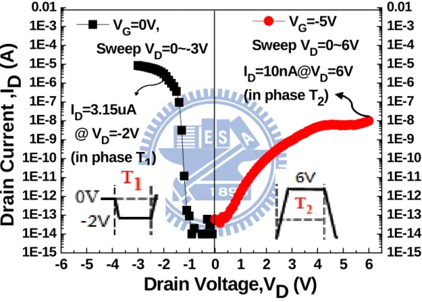
3.3.1 Operating Mode of P-N+ Diode
Figure 3.8 shows two different modes of measurement scale. On the left hand side of Fig. 3.8, the drain current as a function of the negative drain voltage for the
VG= 0V and VD was varied from 0V to -3V. This bias condition was be used to realize
the current of T1 phase in FBHHI erase and we got ID= 3.15 uA, while the
forward-bias is -2V. In contrast, the right hand side of Fig. 3.8 shows the drain current of T2 phase which is a function of the positive drain current and VD was swept from
0V to 6V, the bias condition is equal to BTBHHI erase. The ID is only near 10 nA
even if VD= 6V, so we can compare the currents from different operating modes to
feel the benefits of FBHHI.
3.3.2 The Comparison with FBHHI and BTBHHI Erase
We have known that FBHHI has a better erase speed and enough erasing holes even if at low drain bias. By using multi-cycle pulse series, it only used a half of erase
time (Fig. 3.9) to stress high voltage on the cell and remaining time is be used to generate the operating carriers. As a consequence, multi-cycle pulse series can
enhance the operating speed and reduce the stress time because the mechanism of generated carriers in Fig. 3.10 are far away from the SiO2/Si interface while we
forward-bias the current at p-n+ diode. At T2 phase of FBHHI, we set the drain and
gate voltages equal to BTBHHI erase, then it is easy to compare the results with two
3.3.3 Reliability for FBHHI
A large drain current will induce some problems about junction leakage or
breakdown, but Fig. 3.11 will solve the concern about forward-bias current. We attempted to stress device under a long-term forward mode on the p-n+ diode. The
result in Fig. 3.11 exhibits the stable value of leakage current and threshold voltage at VD= -2V, even if it is until a thousand seconds. Generally, a suitable diode current will
not destroy the implant p-n+ junction and will not cause an increase of the leakage current through the diode. In other words, threshold voltage was not disturbed while
the drain voltage is negative and the storage node was not be erased at T1 phase.
In chapter 4, we will discuss the oxide degradation and interface traps under different erase conditions. It shows that FBHHHI erase can reduce the oxide decay. In
[14], the positive oxide charge assisted tunneling was dominated to be a serious SILC in a hot hole stressed cell. We estimated the negative bias at T2 phase can annihilate
Fig. 3.1 (a) The conventional unit-cycle pulse series for CHEI or BTBHHI. (b) The multi-cycle pulse series for FBEI or FBHHI.
(a)
(b)
Fig. 3.2 The operation scheme and timing diagram for (a) FBEI program and (b) FBHHI erase. The FBEI pulse series were combined with the same pulse width, but the FBHHI series used a varying pulse width.
Fig. 3.3 The characteristics of FBEI as a function of VD,low
-3.0 -2.5 -2.0 -1.5 -1.0 -0.5 0.0 0.0 0.2 0.4 0.6 0.8 1.0 1.2 1.4
T
h
res
h
o
ld
vo
lt
ag
e s
h
if
t,
∆∆∆∆V
th(
V
)
V
D,low(V)
V
D,high=4.5V,V
G=6.5V
Period=1us
Pulse width=10ns
T
r=T
f=10ns
(a)
(b)
Fig. 3.4 (a) The characteristics of FBEI as a function of VD,high (b) The characteristics of FBEI as a function of VG
3.0 3.5 4.0 4.5 5.0 5.5 6.0 0.0 0.2 0.4 0.6 0.8 1.0 1.2 1.4 1.6 1.8 2.0
Period=1us
Pulse width=10ns
T
r=T
f=10ns
Thr os ho ld v ol ta g e s h if t,∆∆∆∆ V th (V )V
D,high(V)
V
D,low=-2V,V
G=6.5V
5.0 5.5 6.0 6.5 7.0 7.5 0.8 1.0 1.2 1.4 1.6 1.8 2.0 2.2Period=1us
Pulse width=10ns
T
r=T
f=10ns
T h ro s h o ld v o lt a g e s h if t,∆∆∆∆ V th (V )V
G(V)
V
D,low=-2V,V
D,high=5.5V
Fig. 3.5 The characteristics of FBHHI as a function of VD,low
-5
-4
-3
-2
-1
0
0.6
0.8
1.0
1.2
1.4
1.6
1.8
2.0
2.2
2.4
Period=0.1ms
Pulse width=0.1us~10us
T
r=T
f=10ns
T
h
resh
o
ld
vo
lt
ag
e
sh
if
t,
∆∆∆∆V
th
(V
)
V
D,lowFBHHI V
G=-6V,V
D,high=5V
Fig. 3.6 The programming transient of SSI and FBEI programs for split-gate SONOS with multi-level cell application.
FBEI V
G=6.5V
FBEI V
G=7.5V
FBEI V
G=8.5V
SSI V
G=8.5V
SSI V
G=9.5V
SSI V
G=10.5V
1E-8 1E-7 1E-6 1E-5 1E-4 1E-3 0.01
0.1
1
-0.5
0.0
0.5
1.0
1.5
2.0
2.5
3.0
3.5
4.0
4.5
5.0
5.5
6.0
T h re s h o ld v o lta g e s h ift, ∆∆∆∆ V th (V )Program Time (S)
Dependence of Vth shift on pulse countFBEI: V
D,low/V
D,high= -2/5.5V
SSI:V
D,low/V
D,high= 0/5.5V
Fig. 3.7 The erasing transient of BTBHHI and FBHHI erases for split-gate SONOS with multi-level application.
1E-8 1E-7 1E-6 1E-5 1E-4 1E-3 0.01 0.1
1
10
-6
-5
-4
-3
-2
-1
0
T h re s h o ld v o lt a g e s h if t, ∆∆∆∆ V th (V )Erase time (S)
FBHHI VD,low/VD,high=-2/4V
FBHHI VD,low/VD,high=-2/5V
FBHHI VD,low/VD,high=-2/6V
BTBHHI VD,low/VD,high=0/4V
BTBHHI VD,low/VD,high=0/5V
BTBHHI VD,low/VD,high=0/6V
Used V
Fig. 3.8 Two different modes of measurement for split-gate SONOS.
-6 -5 -4 -3 -2 -1
0
1
2
3
4
5
6
1E-15 1E-14 1E-13 1E-12 1E-11 1E-10 1E-9 1E-8 1E-7 1E-6 1E-5 1E-4 1E-3 0.01 1E-15 1E-14 1E-13 1E-12 1E-11 1E-10 1E-9 1E-8 1E-7 1E-6 1E-5 1E-4 1E-3 0.01V
G=0V,
Sweep V
D=0~-3V
D
ra
in
C
u
rr
e
n
t ,I
D
(
A
)
Drain Voltage,VD (V)
V
G=-5V
Sweep V
D=0~6V
I
D=3.15uA
@ V
D=-2V
(in phase T
1)
I
D=10nA@V
D=6V
(in phase T
2)
Fig. 3.9 By using multi-cycle pulse series, it only used a half of operating time to be stressed at high voltage and remaining time be stressed at low voltage.
Fig. 3.10 The mechanism of multi-cycle pulse series operation. The generation of carrier is far away from the channel and reduces the oxide degradation.
Fig. 3.11 The value of leakage current and threshold voltage at VD=-2V,
even if it is until a thousand seconds.
10-8 10-7 10-6 10-510-4 10-3 10-210-1 100 101 102 103 104 1.0x10² 1.5x10² 2.0x10² 2.5x10² 3.0x10²
Le
a
c
k
a
ge
C
ur
re
nt
(
p
A
)
Total Forward Bias Time (S)
Read:VG=0V,VD=1.8V
T
h
re
s
h
o
ld
V
o
lt
a
g
e
,
V
th
(
V
)
Forward Bias V
D=-2V
0 2 4 6 8 10CC-Vth :I
D=56nA
Chapter 4
The Monitoring of Stored Charges and Oxide
Traps in a Planar SONOS
4.1 Introduction
In this chapter, we will discuss the different operation combinations in a planar SONOS and analyze the reliability issue for a P/E cycling device using different
operating schemes. We will use the charge-pumping techniques to detect the misalignment between the distribution of electrons and holes. The charge distribution
profiling in charge-trapping memory have been studied by various methods of charge-pumping [8][9], but it became more inaccurate after P/E cycles. We will
propose a monitor to understand the hole-electron misalignment and degradation of operation. [10]
4.2 Principle of Charge Profile by Charge Pumping Method
4.2.1 Principle of Charge Pumping Method
The charge pumping method has been widely used for hot-carrier-related reliability characterization in MOSFETs. During a typical charge pumping
measurement, a pulse string is applied to the gate terminal of a MOSFET while the substrate current (commonly called the “charge pumping current”) is monitored.
the substrate when the gate is biased between flat-band and accumulation) with the
trapped minority carriers at the interface (coming from the source/drain when the gate is biased to inversion), to first order the charge pumping current (Icp) is nonzero only
if the high level (Vh) and the base level (Vb) of the gate pulses cover both the
threshold voltage (Vt) and the flat-band voltage (Vfb) [8][16].
Unlike the conventional charge pumping (CP) method, the other two basic ways
of charge pumping test to obtain the profile are demonstrated. First one is the fixed base CP (fixed base level and varying the top level) method with one side of drain (or
source) floating and the other one is the fixed top CP (fixed top level and varying the base level) method with also one side of drain (or source) floating, which are defined
as FVb and FVt, respectively.
In FVb CP method, the setup is shown in Fig. 2.8 (a) in chapter 2, the gate is
applied with a pulse string, as shown in Fig. 2.8 (a), and the Icp can be measured from
drain or source side with source or drain floating respectively. When measuring the charge pumping current Icp,d from the drain side, the minority carrier only contributed
from the drain side and vice versa with Icp,s. Therefore, we can obtain more precise
information about the drain and source side from Icp,d and Icp,s. By combining these
two currents, we can profile the asymmetrical Vt along the channel for both virgin and
programmed cells [9][18]. In FVt CP method, the setup and gate pulse are shown in
Fig. 2.8(b). The equipment setup is similar to FVb CP method instead of the gate pulse
4.2.2 Fixed Base Charge Pumping Method
Figure 4.1 (a) illustrates the Vt profile of a programmed nitride storage memory
cell, which contains a narrow Vt peak near the drain side. Four regions are marked in
this figure, and they are consistent with the Icp curve tested from FVb CP method in
Fig. 4.1 (b). Fig. 4.1 (b) corresponds to the drain or source junction area in Fig. 4.1 (a). After the programming, localized trapped charges enhance the threshold voltage near
drain side, which forms the asymmetrical Vt profile in Fig. 4.1 (a). Therefore, the Icp,d
and Icp,s curves can be shifted toward the right, which corresponds to the regions B
and C in Fig. 4.1 (b). The difference between curves B and C indicates the location and profile of the injected charges. As Fig. 4.1 (b) shows, the injection is closer to the
drain side. It needs to be pointed out that Icp keeps shifting rightward in region D,
indicating a Vt peak here. Moreover, Icp,d and Icp,s overlap in this region, which means
the minority carrier coming from drain or source is passing through the peak region under the channel. For this reason, the equivalent interface traps are sensed and
contribute the same Icp,d and Icp,s. Thus, in FVb CP method, data obtained in region D
cannot be used to extract the exact profile of Vt in large current region. We can,
however, extract the accurate location using this method.
4.2.3 Fixed Top Charge Pumping Method
On the other hand, the equipment setup is similar to FVb CP method instead of
the gate pulse string which is fixed on a constant level upon the threshold voltage. In
contrast, the Icp curve shift caused by the Vt peak, takes place in the low current
and Fig. 4.1 (b) also can be seen herein. Icp in region D can be used to extract the
accurate profile of narrow Vt peak due to its low testing current. However, Vh is set
larger than the highest Vt along the whole channel, and Icp current tested from drain
and source are identical. FVt CP method can only extract the width and value of
narrow Vt peak but cannot be used to identify the location.
4.3 The Monitoring of Stored Charges for a Cycled Cell
4.3.1 The Correlation Between Stored Charges and I
CPin FV
bCP
Method
Figure 4.3 shows the charge-pumping current measurement to identify the
trapping charges and oxide traps with the source side floating in a planar SONOS. The
curve in ICP plot (Fig. 4.3) shows the existence of injected holes (∆ICP,h), injected
electrons(∆ICP,e), and oxide traps (∆ICP,Nit) in dielectric layer after P/E cycles. The
charge distribution profiling can be found by calculating the correlation between the
injected charges and ICP curve deviation [19][20]. These profiling methods can not be
used to investigate the residue charges in P/E cycling device while they used the other
measurement methods, e.g. GIDL, ID-VG etc., in [21][22].
We will propose a new concept to investigate the complex stored charges condition. In FVb CP method, the cycling ICP curve apparently deviates from fresh ICP
curve as a result of the injected charges. The curve shift presented the amount of the charge in the nitride or oxide. Finally, we used a new area parameter A to discuss the
MAX CPo h CP
V
I
LI
x
=
(
)
/
,dx
dV
dV
I
d
qfW
N
h h CP e N∆
=
1
,4.3.2 Derivation of the Area Parameter
Figure 4.4 shows the difference of ICP,d curve at fresh state and one time program
state in a planar SONOS. The area Ao in the shaded region represents the total stored
electrons in the nitride while the device was only programmed once. The area Ao was
compared with the fresh state ICP(fresh) and one time program state ICP(1@pro).
(1)
In [10], equations used in FVb to calculate the NN,e(x) versus x curve are as
follows:
(2)
(3)
where q is electron charge, f is the frequency of the pulse, W is the effective channel
width, L is channel length, and NN,e(x) is the trapping electrons density in the nitride.
From these equations, we can derive the total charges Qtotal in nitride by integrating
the NN,e(x) from 0 to L. Comparing (2) and (3), we can derive
(4)
[
]
h I V CP CP oI
fresh
I
pro
dV
A
MAX CP h∫
−
=
) ( 0 ,)
@
1
(
)
(
CP CP I e N MAX CPo L e N totalN
I
dI
I
L
dx
x
N
Q
MAX CP)
(
)
(
, 0 , , 0 ,∫
∫
=
=
q
C
C
I
V
C
C
N
N OX CP h N OX e N)
(
)
(
,+
∆
=
[
]
, ( ) , 0(
)
(
)
(
)
h CP MAX V I CP CP h N e hQ
−+ +≈
A cycles
=
∫
I
fresh
−
I
cycles dV
The trapped electron density NN,e(x) is then calculated using the Vh shift ∆Vh(ICP)
[10] ; that is
(5)
This means that the trapping charges were stored near the SiO2/Si3N4 interface.
Then, the total charge can be given by:
(6)
Then, we have the total charges in the nitride:
(7)
Finally, we can use the equation (7) to estimate the number of stored charges in
the nitride with an area parameter A while the cell is at the one time programming state or any P/E cycled state.
(8) (9)
∫
∫
∆
•
+
=
+
∆
=
) ( 0 , 0 , , Pr , ,)
(
)
(
)
(
)
(
MAX CP MAX CP I Vh h h CP N OX N OX MAX CPo CP I N OX CP h N OX MAX CPo total odV
V
I
q
C
C
C
C
I
L
dI
q
C
C
I
V
C
C
I
L
Q
∫
∆
≈
) ( 0 ,)
(
MAX CP I Vh h h CP totalI
V
dV
Q
[
]
h I V CP CP o time oA
I
fresh
I
pro
dV
Q
MAX CP h∫
−
=
≈
) ( 0 1 @ Pr ,)
@
1
(
)
(
4.3.3 The Correlation Between Stored Charges and Area Parameter
First, it was known that the area parameter is related to the stored charges during
any cycled state. The Ao was a basic parameter to compare the A(cycles) at any P/E
cycled state. Fig. 4.3 shows that the injected holes (NN,h) raise up the ICP curve and
decrease the value of A(cycles) in equation (9) while the ICP(cycle) increased. On the
other hand, the injected electrons will suppress the ICP curve and increase the value of
A(cycles). In Fig. 4.3, ∆NOX,it presents the increase of the oxide traps in term of P/E
cycles and it will increase the value of ICP,MAX when the oxide was degraded.
Generally, we may draw a relationship. i.e.,
(10)
From which we can utilize the ∆A/Ao to analyze the condition of hole-electron
misalignment under different operating schemes and the erasing efficiency of
BTBHHI and FBHHI schemes.
4.4 Experimental Results and Discussion
4.4.1 The Basic Operation Conditions of Different Operating
Schemes
Table 4.1 is a combination of different program/erase schemes and the applied biases in a planar SONOS. For program, we used the same VG and VD,high and
programming time to emphasize the different pulse series mode in operating scheme.
it OX h N e N O O
N
N
N
A
A
cycles
A
A
, , ,1
1
)
(
∆
∝
∝
∝
−
=
∆
For erase, we keep the same window margin of 2V while BTBHHI or FBHHI are
used. The endurance of various operation combinations is shown in Fig. 4.5 and we found the window margin was closed and Vth,low was raised by accumulated electrons
while using the BTBHHI erase in Fig. 4.5 (a). Nevertheless, FBHHI can keep the stable window margin, even if it is until one thousand cycle times in Fig. 4.5 (b).
4.4.2 The Experiment Results of FV
bCP Method
Figures 4.6 (a) and (b) show the fix base charge-pumping method for CHEI/BTBHHI cycle and FBEI/BTBHHI cycle, with different cycling time on programming state to do the test. We can get the Ao from fresh ICP,d and 1@Pro ICP,d to
know the total injected electrons after first program. The stored charges in the nitride with P/E cycling were complicated, and we estimated that the non-recombined
electrons at erase state were accumulated, and the holes accumulated above the
overlapping region between the gate and drain. The Α(cycles) was reduced while more holes accumulated at the programmed state.
Generally, we already know the number of total injected electrons by Ao
parameter and then we calculated the ∆A/Ao in different cycling times to investigate
the hole-electron misalignment and operating scheme. In Fig. 4.6, at first, we found the ICP,MAX increased rapidly by using CHEI program, it means that CHEI program
made more interface traps in bottom oxide than FBEI program. For FBHHI erase in
Fig. 4.7, we detected that the value of ∆ICP,MAX was suppressed, in comparison with
Next, we show the variation of ∆A/Ao with increasing P/E cycles in four
operating conditions, as show in Fig. 4.8. Mainly, FBHHI can inject more holes to the nitride, leading to the excess holes accumulated even at the programed state.
Comparing the electron-hole misalignment in Fig. 4.8, FBEI can reduce more accumulated holes than CHEI because its injected electrons are near the drain side by
using FBEI program [5]. Fig. 4.9 was used to know which operating scheme will make even more oxide degradation, and it shows that FBEI/FBHHI be the best P/E
operation as a result of a slope of the increasing ∆ICP,MAX/ICPo,MAX was suppressed.
Basically, the misalignment makes the electrons accumulation in the channel, which can not be recombined by the injected holes. Both electrons and holes
accumulated in the channel will change the drain current flowing path and the electric field in the channel, resulting in the impact ionization position move toward into the
channel, making the mismatch more serious[23][24][25][26]. From the experimental results, FBEI and FBHHI can suppress the oxide degradation in comparison to
conventional operating scheme and FBEI/FBHHI also reduced the misalignment in the trapping memory.
(a)
(b)
Fig. 4.1 (a) The VT profile in a programmed nitride storage memory cell.
(a)
(b)
Fig. 4.2 (a) The VT profile in a programmed nitride storage memory cell.
Fig. 4.3 The schematic FVb charge-pumping current curves related to the trapping charges and interface traps for a planar SONOS.
Fig. 4.4 The difference of ICP,d curves for fresh state and one time program
state in a planar SONOS. The area Ao in the shade region represents
the total stored electrons in the nitride after the first time
N
O
N
N,hN
N,eN
OX,itN
O
N
N,hN
N,eN
OX,it1 10 100 1000 3.0 3.5 4.0 4.5 5.0 5.5 6.0 6.5 P/E cycle
T
h
re
s
h
o
ld
V
o
lt
a
g
e
,V
T H(
V
)
Vth,high-CHEI/BTBHHI Vth,low-CHEI/BTBHHI Vth,high-FBEI/BTBHHI Vth,low-FBEI/BTBHHI(a)
1 10 100 1000 3.0 3.5 4.0 4.5 5.0 5.5 6.0 6.5 P/E cycleT
h
re
s
h
o
ld
V
o
lt
a
g
e
,V
T H(
V
)
V
th,high-CHEI/FBHHI
V
th,low-CHEI/FBHHI
V
th,high-FBEI/FBHHI
V
th,low-FBEI/FBHHI
(b)
Fig. 4.5 The endurance for planar SONOS with different operation combinations.
(a)
(b)
Fig. 4.6 The ICP,d versus VHIGH for a planar SONOS with (a)
CHEI/BTBHHI cycle and (b) FBEI/BTBHHI cycle during different cycling times by using fix base charge-pumping method.
-4 -2 0 2 4 6 8 0.00E+000 6.00E-011 1.20E-010 1.80E-010 2.40E-010 3.00E-010 3.60E-010 Fresh ICP,d 1@Pro ICP,d 10@Pro ICP,d 100@Pro I CP,d 400@Pro ICP,d 1000@Pro ICP,d
I
CP ,d(
A)
V
HIGHCHEI/BTBHHI
V s=floating V D=0V -4 -2 0 2 4 6 8 0.00E+000 6.00E-011 1.20E-010 1.80E-010 2.40E-010 V s=floating VD=0V Fresh ICP,d 1@Pro ICP,d 10@Pro ICP,d 100@Pro ICP,d 400@Pro I CP,d 1000@Pro ICP,dI
CP, d(
A
)
V
HIGHFBEI/BTBHHI
(a)
(b)
Fig. 4.7 The ICP,d versus VHIGH for a planar SONOS with (a) CHEI/FBHHI
cycle and (b) FBEI/FBHHI cycle during different cycling times by using fix base charge-pumping method.
-4 -2 0 2 4 6 8 0.00E+000 4.00E-011 8.00E-011 1.20E-010 1.60E-010 2.00E-010 2.40E-010 V s=floating V D=0V Fresh I CP,d 1@Pro ICP,d 10@Pro I CP,d 100@Pro I CP,d 400@Pro I CP,d 1000@Pro I CP,d
I
CP ,d(
A
)
V
HIGHCHEI/FBHHI
-3 0 3 6 9 0.00E+000 6.00E-011 1.20E-010 1.80E-010 2.40E-010 3.00E-010 Vs=floating VD=0VI
CP ,d(
A
)
V
HIGH Fresh ICP,d 1@Pro ICP,d 10@Pro ICP,d 100@Pro I CP,d 400@Pro I CP,d 1000@Pro I CP,dFBEI/FBHHI
Fig. 4.8 The ∆A/Ao versus P/E cycle with four operating combinations.
1
10
100
1000
-150
-100
-50
0
-150
-100
-50
0
CHEI/BTBHHI
FBEI/BTBHHI
CHEI/FBHHI
FBEI/FBHHI
∆∆∆∆
A
/A
o
(%
)
P/E Cycle
Μο
Μο
Μο
Μο
re
N
N,hresidue
Fig. 4.9 The ∆ICP,max/ICPo,max versus P/E cycle with four operating combinations.