國
立 交 通 大 學
光電工程研究所
博士論文
具氮化鎵與氮化鋁鎵布拉格反射鏡之紫
外光波段氮化鎵雷射之特性研究
Study of Ultraviolet GaN-based Laser with
AlN/AlGaN Distributed Bragg Reflectors
研 究 生: 陳 振 昌 Student: Cheng-Chang Chen
指導教授: 郭浩中 博士 Advisor: Dr. Hao-Chung Kuo
施閔雄 博士 Dr. Min-Hsiung Shih
中
具氮化鎵與氮化鋁鎵布拉格反射鏡之紫
外光波段氮化鎵雷射之特性研究
Study of Ultraviolet GaN-based Lasers with
AlN/AlGaN Distributed Bragg Reflectors
研 究 生: 陳 振 昌 Student: Cheng-Chang Chen
指導教授: 郭浩中 博士 Advisor: Dr. Hao-Chung Kuo
施閔雄 博士 Dr. Min-Hsiung Shih
國立交通大學
光
電 工 程 研 究 所
博
士 論 文
A dissertation
Submitted to Institute of Electro-Optical Engineering College of Electrical Engineering and Computer Science
National Chiao Tung University In Partial Fulfillment of the Requirements
For the Degree of Doctor in Philosophy Electro-Optical Engineering
June 2011
Hsin-chu, Taiwan, Republic of China
具氮化鎵與氮化鋁鎵布拉格反射鏡之紫外光波段
氮化鎵雷射之特性研究
研究生:陳振昌
指導教授:郭浩中 博士
施閔雄 博士
國立交通大學光電工程研究所
摘要
由於氮化鎵材料具有直接寬能隙引起大家的關注並且廣泛的製作成各種應用光電 元件像發光二極體與雷射二極體。高亮度的氮化鎵發光二極體使它應用在交通號誌、 液晶顯示器背光源和固態照明的可行性。此外,藍光雷射二極體是其中廣受應用在 高密度的數位儲存工具的光源。本論文旨在研究具二十五對的氮化鎵與氮化鋁鎵布 拉格反射鏡之紫外光波段微型圓盤以及四方晶格之光子晶體氮化鎵雷射。此布拉格 反射鏡具 85%的高反射率。接著我們研究不經深蝕刻或下部蝕刻的製程製做出大小 為4.7μm 的氮化鎵微型圓盤紫外波段光雷射。經過光性量測系統的量測,得到具低 截止功率密度為0.03kW/cm2的雷射。藉由有限差分時域分析模擬我們去研究迴音壁 模態的共振模態。關於在四方晶格的光子晶體雷射,我們觀察到一強雷射訊號從氮 化鎵光子晶體結構而且此訊號是落在布拉格反射鏡結構的高反射波段區內。藉由三 維平面波展開法以及有限差分時域分析模擬,我們去研究此光子晶體的邊帶模態。 接著我們在 n-型的氮化鎵層製做出大面積的氮化鎵準光子晶體奈米柱結構,藉由奈 米壓印微影技術之後在準光子晶體奈米柱結構頂部以再磊晶成長出氮化銦鎵與氮化 鎵結構之成對金字塔狀的量子井。經過光性量測系統的量測,我們觀察到具低截止 功率的紫外光波段訊號且同時具有從量子井產生綠光。我們用有限元素分析法去分 析準光子晶體的雷射模態。接著我們展現了在室溫下從一金屬鍍膜之氮化鎵奈米共 振腔觀察到雷射訊號。我們觀察到了單一模態的紫外波段雷射訊號,其波長約略三 百七十奈米在截止功率0.042kW/cm2.
II
我們也藉由有限元素分析法模擬的方式來分析此鍍金屬的奈米共振腔的雷射模態與 能帶,我們相信此雷射模態是由波導的模態和表面電漿的模態所混合而成的。
Study of Ultraviolet GaN-based Laser with AlN/AlGaN
Distributed Bragg Reflectors
Student: Cheng-Chang Chen Advisor: Dr. Hao-Chung Kuo
Dr. Min-Hsiung Shih
Department of Photonics & Institute of Electro-Optical Engineering National Chiao-Tung University
Abstract
Wide and direct bandgap of GaN-based materials have been attracted much attention for applications such as light emitting diodes (LED) and laser diodes (LD). The high brightness GaN-based light emitting diodes (LEDs) have made it possible to apply in traffic signals, backlight in liquid crystal displays, and solid state lighting. Besides, the blue LD can serve as the light source of high density data storage in high definition digital versatile disk(HD-DVD) which is one of the popular data storage tools. In this thesis, we are focus on the design and fabrication of the optical pumped ultraviolet GaN-based microdisk and square lattice of photonic crystal lasers with 25 pair AlN/AlGaN distributed Bragg reflectors. The distributed Bragg reflector provides a high reflectivity of 85%. We demonstrated a 4.7 μm GaN-based microdisk laser in ultraviolet range without undercut or deeply-etching procedures. Under optical pumping conditions, the lasing action was observed with a low threshold power density of 0.03 kW/cm2. We
also characterized the whispering gallery mode(WGM) profiles of the microdisk with finite-different time-domain simulation. About square lattice of photonic crystal lasers, a strong lasing emission was observed from GaN photonic crystals within high reflectivity region of DBR. The photonic crystal bandedge mode was also characterized with three-dimensional plane-wave expansion (PWE) and finite-difference time-domain (FDTD) simulation. And large-area GaN-based photonic quasicrystal (PQC) nanopillars structure was fabricated on an n-GaN layer by using nanoimprint lithography technology.
IV
The regrown InGaN/GaN multiple quantum wells (MQWs) form nano-pyramid structure on the top of PQC nanopillars. Under optical pump condition, a lasing action was observed at ultra-violet wavelength with an ultralow threshold power, and the green color emission from InGaN/GaN MQWs was also achieved simultaneously. We characterized the lasing mode with finite-element method (FEM) simulation. Then a metal-coated GaN nanostripe laser was operated at room temperature. The ultraviolet lasing mode was observed at a wavelength of approximately 370 nm with a low threshold power density of 0.042 kW/cm2. The lasing mode and band diagram of the metal-coated
nanostripe were also characterized using FEM simulation. We believed that this lasing mode was a combination of waveguide mode and surface plasmon mode.
誌謝
光陰似箭,一轉眼,博士班畢業了,這過程經歷了很多事情,有幾件深刻的事情 都讓我成長很多,真的很謝謝幫助過我的每一個人。首先,很感謝老師們在這五年 間願意細心教導我不論是課業研究上或生活上的大小事。尤其是施老師對於學術嚴 謹的態度讓我相當的佩服,願意花時間教導我種種問題,讓我在處理事情上更加的 細心與謹慎,雖然我偶而依然會有無理頭的出包,但是真的很謝謝老師的包容。也 很感謝郭浩中老師在我博士班過程中最無助的時候沒有放棄我,介紹我拜入施閔雄 老師門下研究與學習。博士班後期很感謝王祐國與蔡耀瑩兩位學弟強大戰力的應援, 結束了我長達三年多無塵室內的孤軍奮戰。 謝謝很關心我及幫助過我的學長,張鴻儒、柯宗憲、高宗鼎、涂博閔、郭柏儀與 鄧至剛學長。也很謝謝我交大的同學,俊榮、清華、碩均、士偉、明峰、一德、閔 安、俊嘉、宗元及瑞晉的幫忙,讓我能在最後順利的度過博士生涯無論是生活上或 課業上。尤其是俊榮、清華及高大哥宗鼎,因為你們的幫助,讓我能順利的完成學 業,謝謝你們。還有一起努力過與幫助過我的學弟,建華、義淵、家華、亭綱、彥 群、延儒、永吉、思維、朝勳、柏孝、政聰、煇閔、佑慶、世邦、鏡學、信助、治 凱、泳詳、志偉、緯宸、仕傑、冠良、嘉塵及子庭與感謝中研院應科中心郭旻彥與 楊怡君小姐。 很感謝台大黃建璋老師、中山賴聰賢老師、中研院應科中心程育人老師、李柏璁 老師及林國瑞老師在口試時對我的指導,真的很謝謝你們的幫忙。 感謝我的父母及家人、因為有你們的支持,讓我能全心全力的完成博士班的學業。 特別感謝清大動機所計算力學實驗室政德、楊倫學長與全體成員及交大電子所 ED309C 全體成員。 最後,這本論文也獻給所有幫助過我的每一個人^^|| 振昌 于 100 年 6 月 10 日 交通大學光電所
VI
CONTENTS
Abstract (in Chinese) I Abstract (in English) III Acknowledgement V Contents VI List of Figures VIII
Chapter 1 Introduction ... 1
1-1 Wide band-gap of nitride-based materials ... 1
1-2 Nitride-based semiconductor lasers ... 3
1-3 Nitride-based materials of the photonic crystals lasers ... 6
1-3-1 2-D photonic crystals band-edge lasers ... 6
1-3-2 2-D photonic crystals nano-cavity lasers ... 9
1-4 Objective of the thesis ... 11
References. ... 12
Chapter 2 Fabrication and Characteristics of GaN–based Microdisk Lasers with Ultraviolet Distributed Bragg Reflectors ... 16
2-1 Operation principle of semiconductor lasers ... 16
2-2 The theory of Distributed Bragg Reflectors(DBR) ... 25
2-2-1 Penetration depth ... 25
2-3 Ultraviolet AlN/AlGaN DBR ... 28
2-3-1 Design and growth of ultraviolet AlN/AlGaN DBR ... 29
2-4 Transfer Matrix Method ... 33
2-4-1 Finite-Difference Time-Domain(FDTD) ... 37
2-4-2 Analysis of reflectance spectra ... 40
2-5 The set up of micro-photoluminescence ... 42
2-6 Fabrication procedures of microdisk lasers ... 43
2-7 Measurement results and analysis ... 48
Chapter 3 Characteristics of GaN-based photonic Crystal Lasers with
Ultraviolet Distributed Bragg Reflectors ... 59
3-1 Bragg diffraction theory ... 60
3-2 Couple wave theory ... 67
3-3 Plane-Wave Expansion Method for photonic band structure ... 79
3-4 Fabrication of GaN-based photonic crystal structure ... 82
3-5 Characteristics of optical pumped photonic crystal lasers ... 86
References. ... 95
Chapter 4 Fabrication and Characteristics of Quasi-photonic Crystal Lasers with color emission of InGaN/GaN MQWs ... 98
4-1 Finite Element Method ... 99
4-2 Fabrication of quasi-photonic crystal with InGaN/GaN MQWs ... 101
4-3 Characteristics of quasi-photonic crystal lasers with color emission ... 106
References. ... 116
Chapter 5 The Study of Metal-coated GaN Nano-stripe Lasers ... 117
5-1 Fabrication of metal-coated GaN nano-stripe ... 117
5-2 Characteristics of optical pumped nano-stripe lasers ... 123
References. ... 131
Chapter 6 Conclusions ... 132
Publication lists. ... 135
Appendix I………..137
VIII
List of Figures
Chapter 1
Figure 1.1 The applications of GaN-based light sources……….2 Figure 1.2 (a) Scanning electron microscope image of the 1.2-mm microdisk(side view of disk). (b) A 1.2μm disk (the inset showing a high-Q mode, taken above threshold……….4 Figure 1.3 (a) Cross-sectional SEM image of the nano-cavity laser. (b) The L-I curve and the lasing spectrum(inset)…………...………...8 Figure 1.4 (a) Schematic structure of the surface-emitting laser with 2D triangular-lattice
structure embedded by the wafer fusion technique. The inset shows the SEM photograph of the triangular-lattice structure. The lattice constant was 0.462 mm. (b) The lasing spectrum of the device under pulsed condition. Emission normal to the substrate surface was detected………...10
Chapter 2
Figure 2.1 An illustration of output power vs. current for a diode laser………19 Figure 2.2 The internal photon number no versus the pump rate P as a function of the
spontaneous emission coefficient β……….24 Figure 2.3 A schematic diagram of DBRs……….26 Figure 2.4 (a)A SEM image of UV DBR from cross-section view. The total thickness of
25-pairs AlN/AlGaN DBR is about 2μm. (b) The SEM image of the epitaxial gain layer with DBR structure from cross-section view………..30 Figure 2.5 (a) Standard full view of the n&k analyzer. (b) Close up of the sample holder
with the moveable contact points……….31 Figure 2.6 Sktch of a multilayer planar waveguide………...34 Figure 2.7 Sketch of the Yee cell………...38 Figure 2.8 Calculated (solid) and measured (dash) reflectivity spectra of ultraviolet
AlN/AlGaN distributed Bragg reflector measured at room temperature with a stop-band width of about 15nm and the center wavelength is 375 nm………41 Figure 2.9 Optical pumping system………...42
Figure 2.10 Fabrication flowcharts: (a) As-grown sample structure. (b) Deposit SiNx film by PECVD. (c) Spin on PMMA. (d) E-beam lithography. (e) Microdisk pattern transfer to SiNx layer……….44 Figure 2.11 Schematic structure of a GaN-based microdisk with AlN/AlGaN DBR……45 Figure 2.12 (a) A SEM image of a GaN microdisk array with different diameters of 7 μm, 4.7 μm, and 3 μm. (b) A magnified SEM image of a 4.7 μm GaN microdisk cavity from the angle-view………47 Figure 2.13 The PL spectrum of undoped GaN layer………49 Figure 2.14 The measured spectra from a microdisk laser below and above threshold
power. The lasing wavelengths of the microdisk are 377 nm and 379 nm…50 Figure 2.15 The light-in light-out curve (L-L curve) from the microdisk laser………….51 Figure 2.16 Comparison of FDTD simulation (red curve) and measurement (blue
curve)……….53 Figure 2.17 (a) The calculated Hz mode profiles for mode A and (b) mode B from
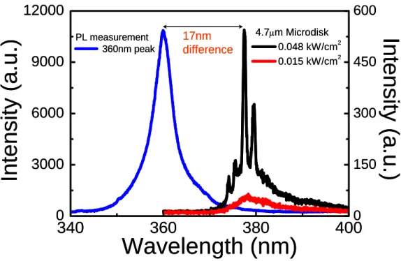
FDTD……….54 Figure 2.18 17 nm difference in wavelength due to the reflection of the UV DBR……..55
Chapter 3
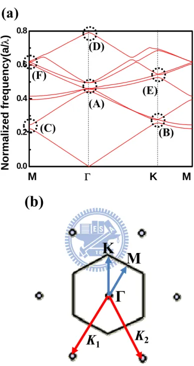
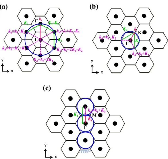
Figure 3.1 (a) The band diagram of photonic crystal with triangular lattice. (b) The schematic diagram of photonic crystal with triangular lattice in reciprocal space……….61 Figure 3.2 Wave vector diagram at points (A), (B), (C) in Figure(a); ki and kd indicate the
incident and diffracted light wave………...63 Figure 3.3 The wave vector diagram at point (A) in vertical direction……….64
X
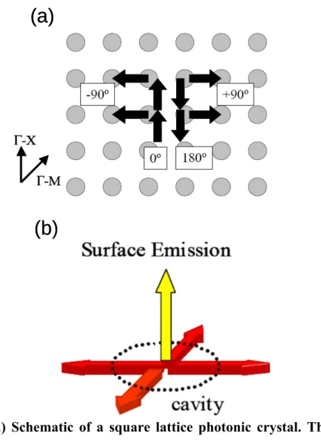
Figure 3.4 (a) Schematic of a square lattice photonic crystal. The two narrow arrows indicate two particular directions Γ-X and Γ-M, and the broad arrows indicate propagating light waves. (b) Schematic showing the propagating directions of the coupled waves………66 Figure 3.5 General multi-dielectric layers show the perturbation of refractive index and
amplitude gain. Z1(x) and Z2(x) are two corrugated functions………68
Figure 3.6 A simple model used to explain Bragg conditions in a periodic waveguide…69 Figure 3.7 Schematic diagram of eight propagation waves in square lattice PC
structure……...……….74 Figure 3.8 Dispersion relationship for TE like modes, calculated using the 2-D
PWEM………..77 Figure 3.9 Sketch of (a) a 2D PC of the triangular lattice and (b) a line defect in a 2D PC..80 Figure 3.10 Fabrication flowcharts: (a) As-grown sample structure. (b) Deposit SiNx film
by PECVD. (c) Spin on PMMA. (d) E-beam lithography. (e) Photonic crystal pattern transfer to SiNx layer………..83
Figure 3.11 (a) Schematic structure of the square photonic crystal patterns with a depth500nm and total square area of a width about 50 μm...84 Figure 3.12 The top view SEM image of the photonic crystal square lattices……….85 Figure 3.13 Measured reflectivity spectrum (blue-dotted curve) of the AlN/AlGaN DBR structure and photoluminescence spectra of above(black curve) and below(red curve) threshold from UV DBR structure at room temperature. This peak wavelength is 372nm which is inside stop-band of DBR……….87 Figure 3.14 The light-in light-out(L-L) curve and linewidth narrowing of the photonic
crystal laser………88 Figure 3.15 Polarization curve of the light emission from the GaN-based photonic
crystals………...90 Figure 3.16 (a)The lasing emission spectra from GaN-based photonic crystals with
different of r/a values. (b) The lasing wavelength versus r/a value of photonic crystal lattices……….91 Figure 3.17 The corresponding band diagram calculated by the PWE method………...93
Figure 3.18 The calculated Hz field by FDTD simulation from (b) top view and (c)
cross-section view………..94
Chapter 4
Figure 4.1 Illustrations of fabrication process of the nanoimprint technology and the regrowth process………..102
Figure 4.2 Schematic structure of GaN-based PQC structure with the regrowth of semipolar{10-11} GaN pyramids and 10-pair In0.3Ga0.7N/GaN (3nm/12nm)
MQW………...103
Figure 4.3 (a) The top-view and (b) The angle-view SEM images of the photonic quasicrystals (PQC) structure. (c) The cross-sectional SEM image of the PQC structure after the regrowth procedure………...105
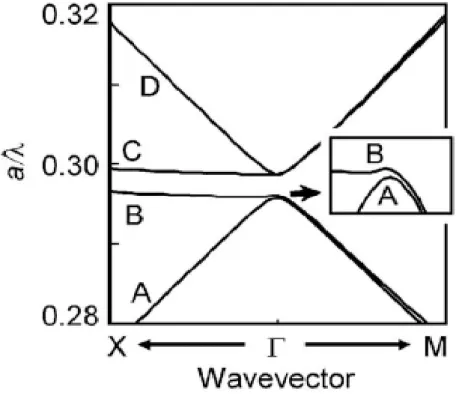
Figure 4.4 The measured spectrum of the sample A from the PQC laser below and above threshold. The lasing wavelength of the PQC is 366nm………107 Figure 4.5 The light-in light-out(L-L) curve and linewidth narrowing of the sample A.108 Figure 4.6 Transmission spectra as a function of normalized frequency a/λ of the PQC
structure………..109 Figure 4.7 Top view of the calculated Hz field by FEM simulation………110
Figure 4.8 The measured spectrum of the sample B with lasing phenomena and green color emission………112
Figure 4.9 The light-in light-out(L-L) curve of the sample B. (c) PL spectra from PQC structure of the sample A(black) and sample B(Green) under the He-Cd 325 nm CW laser pumping………...113 Figure 4.10 PL spectra from PQC structure of the sample A(black) and sample B(Green)
under the He-Cd 325 nm CW laser pumping………...114 Figure 4.11 The photography of the PQC structures on the sample B during the
experiment. And the white light on the center is resulted from the pumping And the white light on the center is resulted from the pumping light source of He-Cd laser.spectra from PQC structure of the sample A(black) and sample B(Green) under the He-Cd 325 nm CW laser pumping………..115
XII
Chapter 5
Figure 5.1 Process flow chart for metal-coated GaN nanostripe……….118 Figure 5.2 SEM image of metal-coated GaN nanostripe (a) Top view of the GaN
nanostripe before deposition of shielding layers. (b) Angle view of one side of the GaN nanostripe before deposition of shielding layers……….120 Figure 5.3 Angle view of the GaN nanostripe after the deposition of SiO2 and aluminum
layers………..121 Figure 5.4 Schematic diagram of metal-coated GaN nanostripe……….122 Figure 5.5 PL spectrum of undoped GaN Layer with and without metal and dielectric
shielding layers………..124 Figure 5.6 PL spectrum of metal-coated GaN nanostripe above (gray) and below (blue)
threshold………125 Figure 5.7 Light-in and light-out curve and the linewidth of lasing peak………...126 Figure 5.8 (a) The Ez mode profile of the nanostripe without shielding layers. (b) The Ez
mode profile of the nanostripe with shielding layers……….129 Figure 5.9 TE Mode band diagram of nanostripe……...……...130
Chapter 1
Introduction
1-1 Wide band-gap of nitride-based materials
Recently, nitride-based materials has been attracting much attention because of their large direct wide band-gap characteristics and can be widely used in various optoelectronic devices[1-4]. According to the large band off-set characteristic of these kinds of III-V wide band-gap materials, which can be utilized in hetero-structure and can provide better carrier confinement to increase the efficiency of the whole structure. Their wide-range band-gap also provides possibility of full-color emission because they cover red, green, and blue emission regions.
Today, blue LEDs are widely used in many applications such as illumination, exterior automotive lighting, full color display, traffic signals, back light of liquid crystal display and etc. The blue LD can serve as the light source of high density data storage (about 25GB/disk, 5 times larger than now) in high definition digital versatile disk (HD-DVD) which is the main stream of next generation data storage. The big market of HD-DVD has shown up the importance of blue LDs. Besides, the blue and violet LDs may have many other possible markets, such as high brightness projector, high speed printer, medical field and others. Figure 1.1 shows the applications of the light sources of the GaN-based materials.
Moreover, nitride-based materials still have lots of advantages such as operation in higher temperature and the higher peak drift velocity for electron. Especially in GaN, the material shows greater characteristic with high bond energy (~2.3eV), high saturation velocity (~2.7*104 cm/s), high breakdown field (~2*106 V/cm) and strong excitonic energy (>50meV) [5]. Because of these advantages, the GaN-based device plays an important role of the high efficiency electro-optic applications and products. However, the problems in GaN, AlN, and its alloy materials are including large defect densities, piezoelectric field effect and spontaneous polarization.
2
(a) Flat panel display (b) Illuminations
(c) Pointer (d) Optical storage
It reveals the most important thing is growing defect-frees material to fabricate high quality and high power devices. Nowadays, the GaN-based materials with its superior properties make it a good candidate for the optoelectronic applications in next generation.
1-2
Nitride-based semiconductor lasers
The research of blue light emitting devices began from the development of gallium nitride light emitting diodes in the early 1970s[6-8]Two decades later, with several efforts devoted to the growth of nitride materials, doping concentration, efficiency of quantum wells, and so on, Nakamura et al.[9]developed the first prototype high-brightness (>100 times greater than previous alternatives, about 1 candela) GaN blue light emitting diodes in 1993. Then, in 1995, they also developed the first successful GaN electron-injection laser[2]. This makes nitride laser diodes begin to step on the road toward the commercial applications of high-information-density storage, laser printer, compact projector, and etc. In these years, the performance of nitride laser diodes has been improved to emit power as high as 100mW at room temperature with a low threshold only 3 kA/cm2[10], and the devices have been already successfully commercialized to be applied to digital versatile disc (DVD). This next-generation DVD would enlarge the storage capacity from 4.7 giga-bytes which current DVD owns to 27 giga-bytes.
High reflectivity nitride-based distributed Bragg reflectors (DBR) are important for the development of GaN-based optical devices such as resonantcavity light-emitting diodes (RCLEDs)[11] and vertical-cavity surface-emitting lasers (VCSEL)[12,13]. In particular, a small optical mode volume can emit a single longitudinal mode with a symmetrically circular beam and a small beam divergence that are superior to the edge emitting lasers and desirable for many practical applications in high density optical storage, and laser printing.
To extend the applications of GaN-based lasers/LEDs into UV region, there are many studies related to the UV GaN-based DBR[14–19]. Bluelight microdisk lasers have also been reported in GaN-based suspended membranes formed by photoelectrochemical etching.[4,20] Figure 1.2 (a) shows the scanning electron microscope(SEM) image of the GaN-based 1.2μm microdisk lasers. And the Figure 1.2 (b) shows the lasing spectrum of the microdisk lasers[4].
4
Figure 1.2 (a) Scanning electron microscope image of the 1.2-mm
microdisk(side view of disk). (b) A 1.2μm disk (the inset showing a
high-Q mode, taken above threshold.
(a)
(b)
(a)
The blue LD can serve as the light source for high density storage system because of its short wavelength. However, due to the applications, the high extraction efficiency of the light source needs to be improved and promoted. In general, there are several methods to increase the light extraction efficiency of GaN-based device such as surface roughness [21,22], and photonic crystal structures[23,24]. The latter method, the photonic crystal structure has a periodic structure with translational symmetry. The periodic structure can exhibit the photonic band gap (PBG) to inhibit the propagation of guided modes[25] and utilize photonic crystal structure to couple guided modes to radiative modes[26-28]. E-beam lithography[29] and laser interference lithography[30] have been used to fabricate the photonic crystal structure. However, NIL is suitable for the mass production of LED devices owing to its good resolution and higher throughput with low fabrication cost.
6
1-3 Nitride-based materials of the photonic crystal lasers
During the last decade, there has been considerable interest in photonic band gap materials or photonic crystals due to their ability to control the properties of light emission and propagation. Many studies have contributed to realize the PC cavities in GaAs-based material by e-beam lithography technique. Since GaN and related nitrides have been the most promising laser diode material in the blue-violet-ultraviolet region, the optical properties of photonic crystal in GaN material is what people want to investigate, recently. As we know, photonic crystal is a dielectric structure arranged in periodic geometry. Like a crystalline solid in electronic band structure. So photonic crystal can exhibit one or more photonic band gaps (PBGs), with frequency in band gap unable to propagate in the crystal. Photonic crystal with photonic band gaps for photons have many advantages in controlling the light emission, wave propagate along specific direction and can be utilized in many optoelectronic devices[31]. For instance, photonic crystal passive waveguide used as low loss channel for light propagation and resonator to keep the whole cavity with high Q characteristic, which can be a promising device in conjunction with Si based and III-V materials communication system. Semiconductor with these unique properties can not only be used as a versatile building block to construct photonic circuitry but also an active medium to control light emission[32]. Two kinds of semiconductor photonic lasers have been demonstrated. One is 2D photonic crystal nano-cavity lasers, and the other is 2D photonic crystal band-edge lasers.
1-3-1 2-D photonic crystal nano-cavity lasers
In 1994, P. R. Berman et al. first presented the mechanism that photonic crystal could be a reflective mirror to form a cavity and achieve the laser operation[33]. Then, in 1999, O. Painter practically demonstrated an optically pumped InGaAs-based 2-D PC nano-cavity laser emitting at 1.55 micrometers[34]. The optical cavity he demonstrated was consisted of a half-wavelength-thick waveguide for vertical confinement and a 2-D PC mirror for lateral localization. A defect was introduced as a nano-cavity because the mode volume was 2.5 cubic half-wavelength widths, approximately 0.03 micrometers, in the 2-D PC to trap photons inside. In 2004, H. G. Park et al. realized the electrically driven single-cell 2-D PC laser with a dominated wavelength at 1519.7nm[35]. They used a sub-micrometer-sized semiconductor post located at the center of the single-cell
photonic crystal resonator to connect bottom electrode and achieved lasing action by current injection. The result is the first current injection report in the world. However, the nitride-based photonic crystal nano-cavity laser never be observed in recently few decades. Figure 1.3 (a) shows the SEM image of the nano-cavity laser and (b) is the typical L-I curve of the monopole-mode laser. Threshold current is 260 μA, and output power indicates the peak value measured at the spectrometer. (Inset) The spectrum is taken at 700 μA.
Fortunately, in 2005, nitride-based photonic crystal nano-cavity membrane emitted at 488nm with quality factor Q of about 800 was reported by Y. S. Choi et al.[36]. They used photo-enhanced chemical etching to form a GaN-based membrane with a total thickness of nearly 140 nm and patterned a photonic crystal nano-cavity on it. Some resonance modes from the nano-cavity with photonic crystal lattice constant of about 180 nm could be observed in the photoluminescence (PL) emission.
8
Figure 1.3 (a) Cross-sectional SEM image of the nano-cavity laser. (b)
The L-I curve and the lasing spectrum (inset).
(a)
(b)
(a)
1-3-2 2-D photonic crystal band-edge lasers
The second one is the photonic crystal band edge laser. According to the DFB theory, light at the photonic band-edge has zero group velocity and forms a standing wave due to 2D DFB effect. Specific band-edges induce not only in-plane coupling via DFB, but also diffraction normal to the PC plane, causing surface emission phenomena. In 1999, Noda et al. reported the electrically driven 2-D PC band-edge laser under pulsed operation [11]. The PC was a triangular-lattice structure composed of InP and air holes, which is integrated with an InGaAsP/InP multiple-quantum-well active layer by a wafer fusion technique. They demonstrated the single-mode, large-area and surface-emitting lasing action, and analyzed the lasing mechanism based on the satisfying of Bragg condition. Then, they further reported the room-temperature (RT) 2D PC band-edge laser under continuous wave (CW) operation in 2004[12]. In 2008, Noda’s group had demonstrated the GaN PCSELs room temperature operation by current injection; they also measured the angle-resolved diagram around Γ band-edge mode [13]. Figure 1.4 (a) Schematic structure of the surface-emitting band-edge laser and the SEM image and (b) is the laser spectrum.
10
Figure 1.4 (a) Schematic structure of the surface-emitting laser with 2D
triangular-lattice structure embedded by the wafer fusion technique.
The inset shows the SEM photograph of the triangular-lattice structure.
The lattice constant was 0.462 mm. (b) The lasing spectrum of the
device under pulsed condition. Emission normal to the substrate surface
was detected.
(b)
(a)
(b)
(a)
1-4 Objective of the thesis
In this thesis, we mainly focus on the study the semiconductor lasers of nitride-based materials including the ultraviolet GaN-based microdisk lasers and 2-D squsre lattice of photonic crystal lasers with AlN/AlGaN distributed Bragg reflectors(DBR). And GaN-based photonic quasicrystal (PQC) nanopillars structure was fabricated on an n-GaN layer by using nanoimprint lithography technology. The regrown InGaN/GaN multiple quantum wells (MQWs) form nano-pyramid structure on the top of PQC nanopillars. Then the study of a metal-coated GaN nanostripe laser operated at room temperature was investigated. About the microdisk lasers and the square lattice of photonic crystal lasers, the study consists of the design, fabrication, and characteristics of the laser. And the detail fabrications of the devices mentioned above were demonstrated. We discussed and analyzed the performance of ultraviolet GaN-based lasers such as threshold characteristics, laser spectrum, and polarization. Furthermore, unique lasing phenomenon, such as specific mode behavior and quality factor in the structure, are also investigated. The detail calculation and simulation are also investigated. For example, in order to understand optical modes of the ultraviolet GaN-based photonic crystal lasers. Plane-wave expansion (PWE) method was used to performed simulations to calculate the band diagram. We also used the finite-difference time-domain(FDTD) simulation to calculate the mode profiles. Moreover, many simulation results are based on FDTD because FDTD method could simulate the real structure more precise. Besides, the lasing modes of the GaN-based photonic quasicrystal (PQC) nanopillars structure and the metal-coated nanostripe were characterized using finite-element method(FEM) simulation. Experimental results show excellent agreement with simulations.
12
References
[1] S. Nakamura, M. Senoh, N. Iwasa, and S. Nagahama, “High-bright InGaN blue, green and yellow light-emitting diodes with quantum well structures,” Jpn. J. Appl.
Phys., vol. 34, pp. L797, 1995.
[2] S. Nakamura, T. Mukai and M. Senoh, “Candela-class high-brightness InGaN/AIGaN double-heterostructure blue-light-emitting diode,” Appl. Phys. Lett.,
64, pp. 1687, 1994.
[3] S. Nakamura, S. Pearton and G. Fasol, The Blue Laser Diode: The Complete Story, Springer-Verlag, Berlin, 2000.
[4] E. D. Haberer, R. Sharma, C. Meier, A. R. Stonas, S. Nakamura, S. P. DenBaars, and E. L. Hu, “Free-standing, optically pumped, GaN/InGaN microdisk lasers fabricated by photoelectrochemical etching,” Appl. Phys. Lett., vol. 85, pp. 5179, 2004.
[5] H. Morkoc, Nitride Semiconductors and Devices, Spring Verlag, Heidelberg, 1999. [6] J. I. Pankove, E. A. Miller, J. E. Berkeyheier, “GaN blue light-emitting diodes,” J.
Luminescence, vol. 5, pp. 84, 1972.
[7] H. P. Maraska, D. A. Stevenson, J. I. Pankove, “Violet luminescence of Mg-doped GaN,” Appl. Phys. Lett., vol. 22, pp. 303, 1973.
[8] J. I. Pankove, “Blue anti-stokes electroluminescence in GaN,” Phys. Rev. Lett., vol.
34, pp. 809, 1975.
[9] S. Nakamura, M. Senoh, S. Nagahama, N.Iwasa, T. Yamada, T. Matsushita, Y. Sugimoto, and H. Kiyoku, “Room-temperature continuous-wave operation of InGaN multi-quantum-well-structure laser diodes with a long lifetime,” Appl. Phys. Lett., vol. 70, pp. 868, 1997.
[10] S. Nakamura, M. Senoh, S. Nagahama, N. Iwasa, T. Yamada, T. Matsushita, H. Kiyoku, Y. Sugimoto, T. Kozaki, H. Umemoto, M. Sano, and K. Chocho,
“InGaN/GaN/AlGaN-based laser diodes with modulation-doped strained-layer superlattices grown on an epitaxially laterally overgrown GaN substrate,” Appl.
[11] M. Diagne, Y. He, H. Zhou, E. Makarona, A. V. Nurmikko, J. Han, K. E. Waldrip, J. J. Figiel, T. Takeuchi, and M. Krames, “Vertical cavity violet light emitting diode incorporating an aluminum gallium nitride distributed Bragg mirror and a tunnel junction,” Appl. Phys. Lett., vol. 79, pp. 3720, 2001
[12] T. C. Lu, S. W. Chen, L. F. Lin, T. T. Kao, C. C. Kao, P. Yu, H. C. Kuo, S. C. Wang, and S. Fan, “GaN-based two-dimensional surface-emitting photonic crystal lasers with AlN/GaN distributed Bragg reflectors,” Appl. Phys. Lett., vol. 92, pp. 011129, 2008.
[13] T. C. Lu, C. C. Kao, H. C. Kuo, G. S. Huang, and S. C. Wang, “CW lasing of current injection blue GaN-based vertical cavity surface emitting laser,” Appl. Phys.
Lett., vol. 92, pp. 141102, 2008.
[14] C. G. Moe, Y. Wu, J. Piprek, S. Keller, J. S. Speck, S. P. DenBaars, and D. Emerson, “Increased power from deep ultraviolet LEDs via precursor selection,” phys. Sat. Sol.
(a), vol. 203, pp. 1915, 2006.
[15] Z. L. Xie, R. Zhang, B. Liua, X. L. Ji, L. Li, C. X. Liu, R.L. Jiang, H. M. Gong, H. Zhao, P. Han, Y. Shi, and Y. D. Zheng, “High reflectivity AlGaN/AlN DBR mirrors grown by MOCVD,” J. Crystal Growth, vol. 298, pp. 691, 2007.
[16] T. Jeong, H. H. Lee, S. H. Park, J. H. Baek1, and J. K. Lee, “InGaN/AlGaN Ultraviolet Light-Emitting Diode with a Ti3O5/Al2O3 Distributed Bragg Reflector,”
Jpn. J. Appl. Phys., vol. 47, pp. 8811, 2008.
[17] E. Feltin, J. F. Carlin, J. Dorsaz, G. Christmann, R. Butte , M. Laugt, M. llegems, and N. Grandjean, “Crack-free highly reflective AlInN/AlGaN Bragg mirrors for UV applications,” Appl. Phys. Lett., vol. 88, pp. 051108, 2006.
[18] O. Mitrofanov, S. Schmult, M. J. Manfra, T. Siegrist, N.G. Weimann, A.M. Sergent, and R.J. Molnar, “High-reflectivity ultraviolet AlGaN/AlGaN distributed Bragg reflectors,” Appl. Phys. Lett., vol. 88, pp. 171101, 2006.
[19] A. Bhattacharya, S. Iyer, E. Iliopoulos, A.V. Sampath, J. Cabalu, T.D. Moustakas, and I. Friel, “High reflectivity and crack-free AlGaNÕAlN ultraviolet distributed Bragg reflectors,” J. Vac. Sci. Technol. B, vol. 20, pp. 1229, 2002.
[20] E. D. Haberer, C. Meier, R. Sharma, A. R. Stonas, S. P. DenBaars, S. Nakamura,and E. L. Hu, “Observation of high Q resonant modes in optically pumped GaN/InGaN
14
microdisks fabricated using photoelectrochemical etching,” Phys. Stat. Sol. (c), vol.
2, pp. 2845, 2005.
[21] T. Fujii, Y. Gao, R. Sharma, E. L. Hu, S. P. DenBaars, and S. Nakamura, “Increase in the extraction efficiency of GaN-based light-emitting diodes via surface roughening,” Appl. Phys. Lett., vol. 84, pp. 855, 2004.
[22] R. H. Horng, C. C. Yang, J. Y. Wu, S. H. Huang, C. E. Lee, and D. S. Wuu, “GaN-based light-emitting diodes with indium tin oxide texturing window layers using natural lithography,” Appl. Phys. Lett., vol. 86, pp. 221101, 2005.
[23] V. V. Nikolaev, M. E. Portnoi, and I. Eliashevich, “Photon Recycling White Light Emitting Diode Based on InGaN Multiple Quantum Well Heterostructure,” Phys.
Status Solidi. A, vol. 183, pp. 177, 2001.
[24] H. De Neve, J. Blondelle, P. Van Daele, P. Demeester, R. Baets, and G. Borghs, “Recycling of guided mode light emission in planar microcavity light emitting diodes,” Appl. Phys. Lett., vol. 70, pp. 799, 1997.
[25] M. Boroditsky, T. F. Krauss, R. Coccioli, R. Vrijen, R. Bhat, and E. Yablonovitch, “Light extraction from optically pumped light-emitting diode by thin-slab photonic crystals,” Appl. Phys. Lett., vol. 75, pp. 1036, 1999.
[26] M. Rattier, H. Benisty, E. Schwoob, C. Weisbuch, T. F. Krauss, C. J. M. Smith, R. Houdre, and U. Oesterle, “Omnidirectional and compact guided light extraction from Archimedean photonic lattices,” Appl. Phys. Lett., vol. 83, pp. 1283, 2003. [27] D. Delbeke, P. Bienstman, R. Bockstaele, and R. Baets, “Rigorous electromagnetic
analysis of dipole emission in periodically corrugated layers: the grating-assisted resonant-cavity light-emitting diode,” J. Opt. Soc. Am. B, vol. 19, pp. 871, 2002. [28] David, T. Fujii, R. Sharma, K. McGroddy, S. Nakamura, S. P. DenBaars, E. L. Hu,
C. Weisbuch, and H. Benisty, “Photonic-crystal GaN light-emitting diodes with tailored guided modes distribution,” Appl. Phys. Lett., vol. 88, pp. 061124, 2006. [29] H. Yu, J. Yu, F. Sun, Z. Li, and S. Chen, “Systematic considerations for the
patterning of photonic crystal devices by electron beam lithography,” Opt. Commun., vol. 271, pp. 241, 2007.
[30] L. Vogelaar, W. Nijdam, H. A. G. M. van Wolferen, R. M. de Ridder, F. B. Segerink, E. Fluck, L. Kuipers, and N. F. vanHust, “Large area photonic crystal
slabs for visible light with waveguiding defect structures: Fabrication with focused ion beam assisted laser interference lithography,” Adv. Mater., vol. 13, pp. 1551, 2001.
[31] M. Notomi, “Theory of light propagation in strongly modulated photonic crystals: Refractionlike behavior in the vicinity of the photonic band gap,” Phys. Rev. B, vol.
62, pp. 10696, 2000.
[32] C.M. Lai, H. M. Wu, P. C. Huang, S. L. Peng, “Single mode stimulated emission from prismlike gallium nitride submicron cavities,” Appl. Phys. Lett., vol. 90, pp. 141106, 2007.
[33] P. R. Berman, New York:Academic, 1994.
[34] O. Painter, R. K. Lee, A. Scherer, A. Yariv, J. D. O`Brien, P. D. Dapkus, I. Kim, “Two-dimensional photonic band-gap defect mode laser,” Science, vol. 284, pp. 1819, 1999.
[35] H. G. Park, S. H. Kim, S. H. Kwon, Y. G. Ju, J. K. Yang, J. H. Baek, S. B. Kim, Y. H. Lee, “Electrically Driven Single-Cell Photonic Crystal Laser,” Science, vol. 305, pp. 1444, 2004.
[36] Y. S. Choi, K. Hennessy, R. Sharma, E. Haberer, Y. Gao, S. P. DenBaars, C. Meier, “GaN blue photonic crystal membrane nanocavities,” Appl. Phys. Lett., vol. 87, pp. 243101, 2005.
[37] M. Imada, S. Node, A. Chutinan. and T. Tokuda, “Coherent two-dimensional lasing action in surface-emitting laser with triangular-lattice photonic crystal structure,”
Appl. Phys. Lett., vol. 75, pp. 316, 1999.
[38] D. Ohnishi, T. Okano, M. Imada, and S. Node, “Room temperature continuous wave operation of a surface-emitting two-dimensional photonic crystal diode laser,” Opt.
Express, vol. 12, pp. 1562, 2004.
[39] Hideki Matsubara, Susumu Yoshimoto, Hirohisa Saito, Yue Jianglin, Yoshinori Tanaka, Susumu Noda, “GaN Photonic-Crystal Surface-Emitting Laser at Blue-Violet Wavelengths,” Science, vol. 319, pp. 445, 2008.
16
Chapter 2
Fabrication and Characteristics of GaN-based Microdisk
Lasers with Ultraviolet Distributed Bragg Reflectors
2-1 Operation principle of semiconductor lasers
Carrier density rate equation
For the double heterostructure(DH), the injected current provides a generation term, and various radiative and nonradiative recombination process as well as carrier leakage provide recombination terms. Thus, we can write the carrier density rate equation,
dN Ggen Rrec
dt = − (2.1)
where N is the carrier density (electron density), Ggen is the rate of injected electrons and
Rrec is the ratio of recombining electrons per unit volume in the active region. Since
q I
i
η
are electrons per second being injected into the active region,
qV I G i gen η = , where V is the volume of the active region. The recombination process is complicated and several mechanisms must be considered. Such as, spontaneous recombination rate, Rsp ~ BN2,
nonradiative recombination rate, Rnr, carrier leakage rate, Rl, (Rnr + Rl = AN+CN3), and
stimulated recombination rate, Rst. Thus we can write Rrec = Rsp + Rnr + Rl +Rst. Besides,
N/τ ≡ Rsp + Rnr + Rl, where τ is the carrier lifetime. Therefore, the carrier density rate
equation could be expressed as
i st I dN N R dt qV
η
τ
= − − (2.2)Photon density rate equation
Now, we describe a rate equation for the photon density (Np), which includes the
photon generation and loss terms. The photon generation process includes spontaneous recombination (Rsp) and stimulated recombination (Rst), and the main photon generation
term of laser above threshold is Rst. Every time an electron-hole pair is stimulated to
Vp, is usually larger than the active region volume occupied by electrons, V, the photon
density generation rate will be [V/Vp]Rst not just Rst. This electron-photon overlap factor,
V/Vp, is generally referred to as the confinement factor (Γ). Sometimes it is convenient to
introduce an effective thickness (deff), width (weff), and length (Leff) that contains the
photons. That is, Vp=deffweffLeff. Then, if the active region has dimensions, d, w, and La,
the confinement factor can be expressed as, Γ=ΓxΓyΓz, where Γx = d/deff, Γy = w/weff, Γz =
La/Leff. Photon loss occurs within the cavity due to optical absorption and scatting out of
the mode, and it also occurs at the output coupling mirror where a portion of the resonant mode is usually couple to some output medium. These net losses can be characterized by a photon (or cavity) lifetime (τp). Hence, the photon density rate equation takes the form
p p st sp sp p dN N R R dt = Γ + Γβ − τ (2.3)
where βsp is the spontaneous emission factor. As to Rst, it represents the
photon-stimulated net electron-hole recombination which generates photons. This is a gain process for photons. It is given by
p p st g p gen dN N R v N dt t Δ ⎛ ⎞ = = = ⎜ ⎟ Δ ⎝ ⎠ g (2.4) where vg is the group velocity and g is the gain per unit length.
Now, we rewrite the carrier and photon density rate equations i g p I dN N v N dt qV
η
τ
= − − g (2.5) p g p sp sp p p dN N v N R dt = Γ g + Γβ −τ (2.6) Threshold gainIn order for a mode of laser to reach threshold, the gain in the active section must be increased to the point when all the propagation and mirror losses are compensated. Most laser cavities can be divided into two general sections: an active section of length La and
a passive section of length Lp. For a laser, at the threshold, the gain is equal whole loss in
the cavity, which includes cavity absorption and mirror loss. For convenience the mirror loss term is sometimes abbreviated as, αm ≡ (1/2L) ln(1/R1R2). Noting that the cavity life
18
time (photon decay rate) is given by the optical loss in the cavity, 1/τp = 1/τi + 1/τm =
vg(αi +αm). Thus, the threshold gain in the steady state can be expressed with following
equation 1 2 1 1 1 ln 2 i m i g p v L R R α α α τ ⎛ ⎞ Γ = + = = + ⎜ ⎟ ⎝ ⎠ th g (2.7) where αi is the average internal loss which is defined by (αiaLa + αipLp)/L (i.e.,αiaLa and
αipLp are loss of active region and passive section, respectively), and R1 and R2 is the
reflectivity of top and bottom mirror of the laser cavity, respectively.
Output power versus driving current
The characteristic of output power versus driving current (L-I characteristic) in a laser diode can be realized by using the rate equation Eq. (2.5) and Eq. (2.6). Consider the below threshold (almost threshold) steady-state (dN/dt = 0) carrier rate equation, the Eq. (2.5) is given by i thI Nth
qV
η
τ
= . While the driving current is above the threshold, the carrier rate equation will be
( th) i g p I I dN v N dt
η
qV − = − g (2.8) From Eq. (2.8), the steady-state photon density above threshold where g = gth can becalculated as i( th) p g th I I N qv V
η
− = g (2.9)The optical energy stored in the cavity, Eos, is constructed by multiplying the photon
density, Np, by the energy per photon, hν, and the cavity volume, Vp. That is Eos = NphνVp.
Then, we multiple this by the energy loss rate through the mirrors, vgαm = 1/τm, to get the
optical power output from the mirrors, P0 = vgαmNphνVp. By using Eq. (2.7) and Eq. (2.9),
and Γ=V/Vp, we can write the output power as the following equation
m ( ) O i th i m h P I I q α ν η α α ⎛ ⎞ = ⎜ ⎟ − + ⎝ ⎠ (2.1 0) Now, by defining m i m i d α α α η η +
PO d h (I Ith) (I>I )th
q ν η
= − (2.11) Thus, the ηd can be expressed as
O (I>I ) d th dP q h dI η ν ⎡ ⎤ = ⎢ ⎥⎣ ⎦ (2.12) In fact, ηd is the differential quantum efficiency. Besides, dPo/dI is defined as the slope
efficiency,Sd,Figure 2. shows the illustration of output power vs. current for a diode laser.
Below threshold, only spontaneous emission is important; above threshold, the stimulated emission power increases linearly with the injection current while the spontaneous emission is clamped at its threshold value.
Figure 2.1 An illustration of output power vs. current for a diode laser.
I
thI
P
o⎟⎟
⎠
⎞
⎜⎜
⎝
⎛
+
=
2 11
ln
2
1
R
R
L
i thα
g
spontaneous emission
section
laser oscillation
section
spontaneous
emission
q
I
h
P
o d/
/
Δ
Δ
=
ν
η
I
P
S
o dΔ
Δ
=
P
Δ
I
Δ
I
thI
P
o⎟⎟
⎠
⎞
⎜⎜
⎝
⎛
+
=
2 11
ln
2
1
R
R
L
i thα
g
spontaneous emission
section
laser oscillation
section
spontaneous
emission
q
I
h
P
o d/
/
Δ
Δ
=
ν
η
I
P
S
o dΔ
Δ
=
P
Δ
I
Δ
20
Coupling Efficiency of Spontaneous Emission into a Lasing Mode[1]
In a conventional semiconductor laser, only a very small part of the spontaneous emission is coupled into a single-lasing mode. That is because the radiation pattern of spontaneous emission is isotropic, a substantial part of the spontaneous emission is not coupled to the guided modes in an active waveguide with a small acceptance angle. Furthermore, the spontaneous emission spectral linewidth is broader than the linewidth of the longitudinal mode; therefore, a substantial part of the spontaneous emission is not coupled to a lasing mode. That is, the coupling efficiency of spontaneous emission (β) usually is considerably small for typical laser diodes.
Suppose an active volume V of semiconductor laser, which is much larger than the cubic of optical length, is enclosed by “perfect reflector”. The number of modes per unit frequency interval is given by 8
π
v V2ε
3/2/c3. If we assume the active dipoles aredistributed uniformly in the volume V and are randomly oriented, the coupling efficiency of spontaneous emission into each mode is identical. The total spontaneous emission rate is given by 2 2 3/2 2 3/2 2 3 2 2 2 3 0 8 2 8 4 ( ) c c sp c v V g N N v V R N g dv c v v c π ε π ε γ π Γ ≡ = = − + Γ
∫
(2.13) Here g is the electric dipole coupling constant and a Lorentzian line shape is 2assumed, 2Γ is the spontaneous emission linewidth in rad/s (FWHM), γ is the spontaneous decay rate, and Nc is total minority-carrier number. If the lasing frequency is coincident with gain center v v= 0, the spontaneous emission rate into one lasing mode
cv E is 2 2 c cv g N E = Γ (2.14) From Eq. (2.13) and Eq. (2.14), the coupling efficiency
β
of spontaneous emission into the lasing mode (spontaneous emission coefficient) is calculated as[2]3 4 4 2 3/2 2 3/2 0.025 3/2 4 4 cv sp E c R v V V V λ λ β π ε π λε ε λ ≡ = = ≈ Γ Δ Δ (2.15)
Here Δ
λ
=λ
2Γ/cπ
is the spontaneous emission linewidth in meters (FWHM). If we use the numerical parameters of a typical GaN semiconductor laser, assuming λ=400nm,1/2 2.5
ε
= , Δλ=20nm, and V =1000 m(μ )3, the spontaneous emission coefficientβ
is on the order of 10−5. This means that only one photon of 105 spontaneously emitted
photons could couple into a lasing mode.
Besides equation Eq. (2.15),
β
also could be written as[3]_ 2 3 / (1 ) 3 4 / ( / ) p p p c F F Q F V n β π λ = + = (2.16) where Fp is the Purcell factor, Q is the cavity quality factor, λ is the wavelength of
laser mode, Vc is the effective optical volume of the laser mode, and n is the refractive _
index.
The calculation of the spontaneous emission coupling efficiency[1]
As discussed already, the coupling efficiency of spontaneous emission into a lasing mode can be increased to a value close to 1 for a microcavity semiconductor laser from 10-5 for a conventional semiconductor laser. The characteristics of such a microcavity semiconductor laser would be very different from a conventional semiconductor laser.
The quantum Langevin equation for the (total) electron number operator Nc
∧ is written as[4] 1 ( cv vc) p sp , c sp sp d N P Nc E E n dt β β τ τ ∧ ⎡ − ⎤ ∧ ∧ ∧ ∧ ∧ ∧ ∧ = −⎢ + ⎥ − − + Γ + Γ + Γ ⎢ ⎥ ⎣ ⎦ (2.17) where P is the pump rate, β Nc /τsp
∧
< > is the spontaneous emission rate into a lasing mode, (1 β) Nc /τsp
∧
− < > is the spontaneous emission rate into all other modes except the lasing mode, Ecv
∧
< > and Evc
∧
< > are the stimulated emission and absorption rates per photon, ( Ecv Evc )
∧ ∧
< > − < > is a population inversion parameter, n∧ is the (total) photon number operator, p
∧
Γ , sp
∧
22
process, the spontaneous emission process and stimulated emission or absorption process. The quantum Langevin equations for (total) photon number operator n is written as ∧
( cv vc) c e sp d n E E n N F F dt Q ω β τ ∧ ⎡ ∧ ∧ ⎤∧ ∧ ∧ ∧ = −⎢ − − ⎥ + + + ⎣ ⎦ (2.18) where ωQ is the photon decay rate, F∧ , and Fe
∧
are the noise operators associated with the stimulated emission processes, and the photon decay process.
Let us consider the steady-state (average) solutions of Eq. (2.17) and Eq. (2.18). Using the linear solutions,Nc Nc0 Nc
∧ ∧
= + Δ and n n∧ = 0+ Δn∧, in Eq. (2.17) and (2.18), we obtain 0 0 0 c sp sp sp N P n n β τ τ − − = (2.19) 0 0 0 0 c c sp sp sp N N n Q n β β ω τ τ ⎡ ⎤ −⎢ − ⎥ + = ⎢ ⎥ ⎣ ⎦ (2.20) At pump rates above the threshold, the photon decay rate
ω
/ Q is equal to the net gain Ecv Evc∧ ∧
− (i.e., the stimulated emission gain stimulated absorption loss). nsp is
photon density. Thus,
0, c th sp sp N Q n β ω τ = (2.21) where Nc th0, is the threshold (total) electron number, which is approached by real
electron number Nc0 only when the pump rate is well above the threshold.
At the threshold pump rate, all the pump electrons recombine via spontaneous emission(Pth = Nc th0 , /τsp). The stimulated emission rate Ecv by one photon is equal to
the spontaneous emission so that
Ecv =
β
Pth (2.22)From Eq. (2.21), the threshold pump rate can be calculated as
0, ( / ) sp c th th sp Q n N P ω τ β = = (2.23)
This is an important result suggests that the threshold pump rate can be decreased by increasing
β
.It is obvious from this equation that the real electron number Nc0 never reaches the threshold value Nc th0, as long as the spontaneous emission coefficient
β
is nonzero.From Eq. (2.20), the average electron number Nc0 is given by
2 1/2 0, 0 0, ( 1) [( 1) 4(1 ) ] , 1 2(1 ) , 1 1 c th c c th r r r N N r N r β β β β ⎧ + − + − − ≠ ⎪⎪ − = ⎨ ⎪ = ⎪ + ⎩ (2.24)
where r P P= / th is the normalized pump rate and Nc th0 , =ωτspnsp/Qβ .
From Eq. (2.20), the average photon number n0 is
0 0 0 / / / c sp c sp sp N n Q N n β τ ω β τ = − (2.25) Using Eq.(2.24) in Eq. (2.25), the average photon number n0 is
2 1/2 2 1/2 0 ( 1) [( 1) 4(1 ) ] ( 1) [( 1) 4(1 ) ] / 1 , 1 2(1 ) 2(1 ) , 1 sp sp r r r r r r n n n r β β β β β β ⎧ + − + − − ⎡ − + − + − − ⎤ ≠ ⎪ − ⎢ − ⎥ = ⎨ ⎣ ⎦ ⎪ = ⎩ (2.26)
24
The threshold condition Eq. (2.23) holds when the photon number n0 is much smaller than one at the transparency point. Figure 2. shows the internal photon number n0 versus the pump rate P as a function of the spontaneous emission coefficient
β
, assuming that nsp =1andβ
Pth is the same for each curve with differentβ
value. It is clear the jump of photon number at near threshold is smaller and smaller as the value ofβ
is larger. As theβ
=1, the increase of photon number with the increasing of pump rate becomes linear.
Figure 2.2 The internal photon number n
oversus the pump rate P as a
function of the spontaneous emission coefficient β.
10
-110
010
110
-110
010
110
210
310
410
5Photon number (#)
Pump rate (P/P
th)
β=1 β=0.1 β=0.01 β=0.001 β=0.00012-2 Distributed Bragg Reflectors
The research of blue light emitting devices began from the development of gallium nitride light emitting diodes in the early 1970s[5-7]. Two decades later, with several efforts devoted to the growth of nitride materials, doping concentration, efficiency of quantum wells, and so on, Nakamura et al. developed the first prototype high-brightness (>100 times greater than previous alternatives, about 1 candela) GaN blue light emitting diodes in 1993. Then, in 1995, they also developed the first successful GaN electron-injection laser. This makes nitride laser diodes begin to step on the road toward the commercial applications of high-information-density storage, laser printer, compact projector, and etc. In these years, the performance of nitride laser diodes has been improved to emit power as high as 100mW at room temperature with a low threshold only 3 kA/cm2, and the devices have been already successfully commercialized to be applied to digital versatile disc (DVD). This next-generation DVD would enlarge the storage capacity from 4.7 giga-bytes which current DVD owns to 27 giga-bytes.
2-2-1 Penetration depth[5]
Distributed Bragg reflectors (DBRs) served as high reflecting mirror in numerous optoelectronic and photonic devices such as VCSEL. It is a periodic structure formed by stacking several pairs of two 1/4-lamda-thick layers with different refractive index. Consider a distributed Bragg reflector consisting of m pairs of two dielectric, lossless materials with high- and low- refractive index nH and nL, as shown in Figure 2.. The
thickness of the two layers is assumed to be a quarter wave, that is, L1 =λB/4nH and L2
26
Figure 2.3 A schematic diagram of DBRs.
L
1L
2n
Hn
L1
2
.. .. .. .. .. .. .. .. ..
m
effective reflector
L
penn
ssub
s
tr
at
e
n
oL
1L
2n
Hn
L1
2
.. .. .. .. .. .. .. .. ..
m
effective reflector
L
penn
ssub
s
tr
at
e
n
oMultiple reflections at the interface of the DBR and constructive interference of the multiple reflected waves increase the reflectivity with increasing number of pairs. The reflectivity has a maximum at the Bragg wavelength λB. The reflectivity of a DBR with m
quarter wave pairs at the Bragg wavelength is given by[8]
2 2 1 ( ) 1 ( ) s L o H s L o H p p n n n n R n n n n ⎛ − ⎞ ⎜ ⎟ = ⎜ ⎟ ⎜ + ⎟ ⎝ ⎠ (2.27) where the no and ns are the refractive index of incident medium and substrate. The
high-reflectivity or stop band of a DBR depends on the difference in refractive index of the two constituent materials, ∆n (nH - nL). The spectral width of the stop band is given by
stopband 2 B eff n n λ λ π Δ Δ = (2.28) where neff is the effective refractive index of the mirror. It can be calculated by requiring
the same optical path length normal to the layers for the DBR and the effective medium. The effective refractive index is then given by
2(
1
1
)
1 H L effn
n
n
−=
+
(2.29) The length of a cavity consisting of two metal mirrors is the physical distance between the two mirrors. For DBRs, the optical wave penetrates into the reflector by one or several quarter-wave pairs. Only a finite number out of the total number of quarter-wave pairs are effective in reflecting the optical wave. The effective number of pairs seen by the wave electric field is given by1 tanh(2 ) 2 H L H L H L H L eff n n n n m m n n n n + − ≈ − + (2.30)
For very thick DBRs (m→∞) the tanh function approaches unity and one obtains
1
2
H L H L effn
n
m
n
n
+
≈
−
(2.31)Also, the penetration depth is given by
1 2tanh(2 ) 4 pen L L L mr r + = (2.32) where r = (n1-n2)/ (n1+n2) is the amplitude reflection coefficient.
28
For a large number of pairs (m→∞), the penetration depth is given by 1 2 1 2 4 4 H L H L pen L L L L n n L r n n + + + ≈ = − (2.33)
Comparison of Eq. (2.31) and Eq. (2.33) yields that
1
(
1 2)
2
pen eff
L
=
m
L
+
L
(2.34) The factor of (1/2) in Eq. (2.34) is due to the fact that meff applies to effective number ofperiods seen by the electric field whereas Lpen applies to the optical power. The optical
power is equal to the square of the electric field. The effective length of a cavity consisting of two DBRs is thus given by the sum of the thickness of the center region plus the two penetration depths into the DBRs.
2-3 Ultraviolet AlN/AlGaN DBR
In general, ultraviolet nitride-based DBRs consist of AlInN/AlGaN or AlGaN/AlGaN material system[9]. Especially, for devices containing pure GaN as an active medium, the ultraviolet DBRs cannot employ GaN as the layer materials because of the strong increase of optical absorption below 360 nm. In this section, we report the growth on 2 inch c-sapphire substrates of high-reflectivity AlN/AlGaN DBRs designed for the ultraviolet spectral region. The structures are grown by MOCVD and consist of AlN/Al0.2Ga0.8N system to increase the difference of refractive index in the DBR
structures. The measured peak reflectivity value is 85% for 25-pairs AlN/AlGaN DBRs. Furthermore, the experimental reflectivity spectra are modeled by transfer matrix theory in order to compare the experimental and theoretical results.
2-3-1 Design and growth of ultraviolet AlN/AlGaN DBR
The AlN/AlGaN DBRs were grown in a low-pressure high-speed rotating-disk MOCVD system. Two-inch diameter (0001)-oriented sapphire substrates were used for the growth of DBR samples. During the growth, TMGa and TMAl were used as group III source materials and NH3 as the group V source material. After thermal cleaning of the
substrate in hydrogen ambient for 5 min at 1100 °C, a 30-nm-thick GaN nucleation layer was grown at 500 °C. The growth temperature was raised up to 900 °C for the growth of 3.4μm GaN buffer layer. Then, the AlN/AlGaN DBRs were grown under the fixed chamber pressure of 1.33×10⁴ Pa. The DBR consists of 25-pairs AlN/Al
0.2Ga0.8N
quarter-wavelength layers. By employing in situ optical reflectivity system, the growth rate of the AlN and AlGaN layer can be estimated to be about 0.7 and 2.2 Å/s, respectively. The thicknesses of the total DBR structures were investigated by SEM as shown in Figure 2.4 (a) The schematic structure of the grown DBR and (b) the magnification cross-section SEM image of the 25-pair DBR with the top gain material layer. The reflectivity spectrum of the AlN/AlGaN DBRs was measured by the n & k ultraviolet-visible spectrometer with normal incidence at RT [10-12].
The model used in the n&k 1280 to analyze the raw data is based on the Forouhi-Bloomer Model for n and k. These equations are derived from the quantum theory of the absorption of light and are consistent with the Kramers-Kronig dispersion relationship for n and k. This model is quit general and applies to thin layers of semiconductors, dielectrics, dyes, polymers, as well as metal films. Other tools rely on models such as the harmonic oscillator, Cauchy, Sellmeier, and Tauce quations for n and k. These equations are valid over a very limited range of wavelengths and are difficult to apply to films comprising ”high tech”devices. The Cauchy, Sellmeier, and Tauc models do not satisfy the Kramers-Kronig relationship for n and k. Figure 2.5 shows the set up of the n&k analyzer.
The n&k analyzer can determines those important paprmeters such as thickness, spectra of optical constants (n and k), reflectance (R), interface roughness, and Energy band gap.
30
Figure 2.4 (a) A SEM image of UV DBR from cross-section view. The
total thickness of 25-pairs AlN/AlGaN DBR is about 2μm. (b) The SEM
image of the epitaxial gain layer with DBR structure from cross-section
view.