國 立 交 通 大 學
電信工程學系
碩 士 論 文
利用頻率選擇面設計雙頻可切換
場型之波束天線
Novel Dual-Band Pattern Reconfigurable Reflector
Antennas Using Switching Frequency Selective
Surfaces
研究生:柯智祥
(Chih-Hsiang Ko)
指導教授:鍾世忠 教授
(Dr. Shyh-Jong Chung)
利用頻率選擇面設計雙頻可切換場型之波束天線
Novel Dual-band Pattern Reconfigurable Reflector Antennas Using
Switching Frequency Selective Surfaces
研究生:柯智祥 Student : Chih-Hsiang Ko
指導教授:鍾世忠 博士 Advisor : Dr. Shyh-Jong Chung
國立交通大學
電信工程學系
碩士論文
A Thesis
Submitted to Department of Communication Engineering
College of Electrical and Computer Engineering
National Chiao Tung University
in Partial Fulfillment of the Requirements
For the Degree of Master of Science
In Communication Engineering
September 2008
Hsinchu, Taiwan, Republic of China
I
利用頻率選擇面設計雙頻可切換場
型之波束天線
研究生:柯智祥 指導教授:鍾世忠 博士
國立交通大學電信學系
碩士論文
摘要
隨著無線通訊的發展,有限的頻寬不斷地被數量眾多的無線通訊設備使用及 分割,因此,如何有效地使用通訊頻寬並將其他干擾減至最低將是目前無線通訊設 備在設計上一個重要的課題。可變換場型並集中能量的智慧型天線是一個解決此問 題的好選擇。 在本論文中,我們提出一種新型的雙頻的智慧型天線。利用可改變特性的頻 率選擇平面當做主要的反射面架構,並配合直角反射面天線的運作原理及電路開關 的狀態,設計出三個雙頻的智慧型天線,可使用於 2.45 GHz 及 5.25 GHz 的頻段 中。藉由各面上開關的組合,此天線可以包括許多不同的場型。 第一個天線的反射面只能運作在某一個頻率,因此,對於雙頻的智慧型天線 來說,雙層的反射面設計是必需的,同時也增加了使用體積;而第二個天線的設計 中,將單一反射面設計成可操作在雙頻,如此可減少天線體積,並可減少開關的使 用數量;在第三個天線中,一種更為簡單的雙頻反射面架構被提出,在每一邊僅用 一個長方形的環形共振器,如此可更加簡化天線的複雜度及開關的設計。而在實際 的應用當中,全向性場型跟單一方向性場型的切換是最重要的,因此在以上的設計 中,我們主要專注研究在此兩種場型的特性與切換。II
Novel Dual-band Pattern Reconfigurable Reflector
Antennas Using Switching Frequency Selective
Surfaces
Student : Chih-Hsiang Ko Advisor : Dr. Shyh-Jong Chung Departmentof Communication Enginnering
National Chiao Tung University
A
BSTRACTWith the development of the wireless communication, more and more devices share the limited bandwidth for communication. Therefore, how to reduce the interference from other devices and environment and use the limited bandwidth efficiently is one of the important subjects. A smart antenna which can change radiation patterns and focus the patterns is a good candidate to solve those problems.
In this thesis, a novel dual-band smart antenna is developed. By the switching frequency selective surface, the principle of a right angle corner reflector antenna, and the operation of switches, three dual-band pattern reconfigurable antennas are investigated. The operating frequencies in our design are 2.45 GHz and 5.25 GHz. Through combinations of switches on reflecting walls, multiple radiation patterns can be obtained.
Each reflecting wall of the first proposed pattern reconfigurable antenna operates only at one frequency; therefore, Two-layer reflecting walls are needed here. However, the volume of the completed antenna is about one-wavelength of 2.45 GHz square due to the principle of the corner reflector antenna. In the second proposed antenna, a reflecting wall can operate at two frequencies. As a result, the size of the antenna can be reduced, and the amount of switches can be decreased too. Finally, a dual-band pattern reconfigurable antenna with a simpler structure such as a rectangular loop is developed without the damages to the original properties belonging to the second antenna. Since omni-directional and directional patterns are the most important in application, we mostly focus on those two patterns in our design.
III
Acknowledgement
在這篇碩士論文完成的同時,我首先要感謝的就是我的指導教授鍾世忠博士。我 從專題開始就跟著鍾世忠教授做一些天線方面的研究,雖然一開始有很多不懂的地 方,但是教授他總是會適時地給予指導,讓我可以了解到天線的原理及設計方法; 此外,教授也一直鼓勵我要多看期刊論文,以增加自己的專業知識跟想法,這對我 來說助益是很大的,讓我在短時間內,對於天線的觀念建立起來,使我可以盡早做 研究而順利畢業。因此,真的由衷感謝鍾世忠教授這三年來的指導。 而譚怡揚學長是我另一個要感謝的人,這篇論文的完成,多虧有學長的啟發跟討 論,讓我了解「頻率選擇面」的原理跟設計想法,而學長做的單頻的場型可偏天線 也是本論文的前身,因此學長的幫忙真是不言而喻啊! 當然囉!在我們前膽實驗室中,大家都給了我很多的幫助。什麼都懂的王侑信學 長,在我對於天線觀念及論文不懂的地方,都可以給予教學,讓我突破盲點,我天 線知識的建立他也是功臣之一呢!凌菁偉學姊是算是一開始我最早認識的吧!她從 專題生開始就帶著我們專題生,了解研究生是怎麼做事的;而當我進來實驗室之 後,她也一直很照顧著大家,幫了大家很多的忙,可謂是實驗室之「母」啊!再來 就是林靖凱學長啦!他是我最愛跟他爭論東西的人了,不過也因為可以跟他爭論一 些概念,讓我對一些東西有了不一樣的觀點,而他也很會用手把東西算出來,當初 跟他一起把期中期末考古題打敗的經驗還真是有趣呢!天線組的最後一個學長—莊 肇堂,雖然跟他只認識一年,不過他可是濾波器專門的呢!雷達組的兩位學長:何 丹雄跟林明達學長,可是很辛苦的兩位呢!常常看到他們在為了雷達的事用到很 晚,真是辛苦了! 而不知道該是算跟我同屆還是學長的碩二同學們,真的很開心可以跟你們一起畢 業。超級愛吹噓的蘇邵軒,最後變成我的好車友;聽說之前是系排隊長的王思本, 在實驗室是個宅宅,但是他也是神手本,沒有他調不出來的天線呢;洪傳恩則是最 讓我判若兩人的人,他曾經在我腦中是的正直的少年,沒想到認識他以後,才知道 他一點都不正直,不過,也因為這樣,實驗室多了很多八卦跟樂趣呢!他是我的好 車友啊!而要跟我去騎車環島的馬義翔更是不能不提啊,他可是我畢業後的同行者IV 啊!我的天線也因為有他的幫助,讓我可以及時趕出來,去量測,真是很謝謝他。 再來,電腦通黃天建學長,他真的是無所不能,只要有什麼電腦的問題,問他就對 了啦!而 IC 組的清標學長真的是長不大,雖然跟他沒什麼研究上的交集,不過跟 他聊天還蠻有趣的呢!感覺是好好人的佩宗,常常看到他一個人在焊電路,真是苦 命啊! 再來,就是理論上跟我同屆的三位啦!許少華,號稱許董,是真性情男子,也因 為他相信「實驗室沒有秘密」,而讓他對實驗室真的沒有秘密;賴浩宇,俗稱浩 呆,這個名稱的理由,我想大家都懂了,不過,他真的是一個好好人的超宅宅;池 冠儀,同位語:小池,她是實驗室的幽靈人物,真的超少來的,最常跟他說的話大 概是「快來丟垃圾吧!」,但是她到羽球場上,可是一名猛將呢! 實驗室助理,陳珮華,外號一堆,每個人都叫他不一樣的名字。不過,實驗室有 她真的讓我們少了很多麻煩,雖然他桌上真的超亂,但是她總是可以找到那些東 西,真是太神奇了。而在前幾個月,她也結婚了,就祝她快生吧!XDDDD 真的很開心我可以加入這個前膽微波實驗室(我還是習慣叫「Lab912」),讓我可 以很開心地渡過專題跟研究生的這兩年。
謝謝大家啦!
V
C
ONTENTS
摘要
………. I
A
BSTRACT………. ... II
A
CKNOWLEDGEMENT... III
C
ONTENTS………. ... V
C
ONTENTS OFT
ABLES... VII
C
ONTENTS OFF
IGURES... VIII
C
HAPTER1
I
NTRODUCTION... 1
C
HAPTER2
T
HEORY OFT
HEORY OFC
ORNERR
EFLECTORA
NTENNA ANDF
REQUENCYS
ELECTIVES
URFACE... 7
2-1CORNER REFLECTOR ANTENNA ... 7
2-2FREQUENCY SELECTIVE SURFACE ... 11
C
HAPTER3
D
UAL-B
ANDP
ATTERNR
ECONFIGURABLEA
NTENNA WITHT
WO-L
AYERW
ALLS... 13
3-1ANTENNA CONFIGURATION ... 13
3-2DESIGN OF RECONFIGURABLE FSSSTRUCTURES ... 15
3-3DESIGN OF THE DUAL-BAND PATTERN RECONFIGURABLE REFLECTOR ANTENNA WITH TWO-LAYER WALLS ... 23
3-3-1 Functions of the two more half rectangular loops printed on the inner wall ...23
3-3-2 Interactions between the inner walls and the feeding antenna ...24
3-3-3 Design of the feeding antenna ...25
3-4MEASUREMENT RESULTS ... 28
C
HAPTER4
D
UAL-B
ANDP
ATTERNR
ECONFIGURABLEA
NTENNA WITHS
INGLE-L
AYERW
ALLS... 33
4-1ANTENNA CONFIGURATION ... 33
4-2DESIGN PROCEDURE OF THE DUAL-BAND FSSWALLS ... 35
4-2-1 Spacing between the wall and the feeding antenna ...35
4-2-2 Switching dual-band FSS elements ...37
4-2-3 Design of the feeding antenna ...45
VI
C
HAPTER5
D
UAL-B
ANDP
ATTERNR
ECONFIGURABLEA
NTENNA BYF
OURS
WITCHINGR
ECTANGULARL
OOPS... 52
5-1ANTENNA CONFIGURATION ... 52
5-2DESIGN OF DUAL-BAND PATTERN RECONFIGURABLE STRUCTURES WITH A SINGLE LOOP ... 54
5-2-1 Design of the reflector by a single loop ...54
5-2-2 Design of the feeding antenna ...59
5-3MEASUREMENT RESULTS ... 61
C
HAPTER6
C
ONCLUSION... 66
VII
C
ONTENTS OF
T
ABLES
TABLE I THE IEEE STANDARDS OF 802.11A/B/G/N... 1 TABLE II THE DEFINITIONS OF THE TWO FUNDAMENTAL CASES AND THE SIMULATED AND
MEASURED RESULTS OF THE DUAL-BAND PATTERN RECONFIGURABLE ANTENNA WITH TWO-LAYER WALLS ... 29 TABLE III THE DEFINITIONS OF THE TWO FUNDAMENTAL CASES AND THE SIMULATED
AND MEASURED RESULTS OF THE DUAL-BAND PATTERN RECONFIGURABLE ANTENNA WITH SINGLE-LAYER WALLS ... 48 TABLE IV THE DEFINITIONS OF THE TWO FUNDAMENTAL CASES AND THE SIMULATED
RESULTS OF THE DUAL-BAND PATTERN RECONFIGURABLE ANTENNA BY FOUR RECTANGULAR LOOPS ... 62
VIII
C
ONTENTS OF
F
IGURES
Fig. 1.1. Geometry of a 2-D pattern reconfigurable antenna based on Yagi-Uda antennas.
... 3
Fig. 1.2. Geometry of a 3-D pattern reconfigurable antenna based on Yagi-Uda antennas. ... 4
Fig. 1.3. Geometry of a 3-D pattern reconfigurable antenna by changing feeding locations ... 4
Fig. 1.4. Geometry of a 3-D pattern reconfigurable antenna with circle arrangement of parasitic elements. ... 5
Fig. 1.5. A pattern diversity antenna by changing the induced current distribution on parasitic elements. ... 5
Fig. 2.1. The configuration of a corner reflector antenna. ... 7
Fig. 2.2. The corner reflector with images shown and how they account for reflections. .. 8
Fig. 2.3. Principal plane patterns, |AF|, for a right angle corner reflector. ... 8
Fig. 2.4. Geometry of a three-dimensional corner reflector antenna. ... 9
Fig. 2.5. Geometry of a triple corner reflector antenna. ... 9
Fig. 2.6. Geometry of a corner reflector antenna with the cylindrical corner. ... 10
Fig. 2.7. Geometry of a pattern reconfigurable antenna evolved from Yagi-Uda antennas and corner reflector antennas. ... 10
Fig. 2.8. (a) An electron in filter plane undergoes oscillations driven by source wave. (b) An electron constrained to move along wire cannot undergo oscillations. ... 11
Fig. 2.9. Different shapes of the FSS structures. ... 12
Fig. 3.1. Configuration of the proposed dual-band pattern reconfigurable antenna. ... 13
Fig. 3.2. Geometries of the dual-band FSS structures (a) the outer walls (b) the inner walls ... 15
Fig. 3.3. Current distributions of the FSS structures at 2.45 GHz on (a) two rectangular loops. (b) a switching FSS when the switch is on. (c) a switching FSS when the switch is off. ... 17
IX
Fig. 3.4. Current distributions of the FSS structures at 5.25 GHz on (a) two rectangular loops. (b) a switchable FSS when the switch is on. (c) a switchable FSS when the switch is off. ... 18 Fig. 3.5. The simulation model for designing FSS structures. ... 19 Fig. 3.6. The simulated transmission coefficients at (a) 2.45 GHz (b) 5.25 GHz when the
switches are in ON-state or Off-state. ... 20 Fig. 3.7. The simulated current distributions in the dual-band pattern reconfigurable
reflector antenna at 2.45 GHz (large loops) and 5.25 GHz (small loops) in (a) ON-state. (b) Off-state. ... 21 Fig. 3.8. The comparison of the patterns in = 45o plane in case 2 at 5.25 GHz between
the FSS wall for 5.25 GHz with corner rings and without corner loops. ... 24 Fig. 3.9. The comparison of the patterns in = 45o plane in case 2 at 2.45 GHz between
the switches, S1b、S4b, in off-state and on-state. ... 25
Fig. 3.10. The dual-band feeding antenna with two trident structures. ... 26 Fig. 3.11. The measured and simulated return loss of the dual-band feeding antenna. .... 27 Fig. 3.12. The photo of the complete dual-band pattern reconfigurable reflector antenna. ... 28 Fig. 3.13. The measured and simulated patterns of Case 2 at (a) 2.45 GHz (b) 5.25 GHz. ... 30 Fig. 3.14. The measured and simulated patterns of Case 1 at (a) 2.45 GHz (b) 5.25 GHz. ... 31 Fig. 4.1. The configuration of the proposed dual-band pattern reconfigurable antenna. .. 33 Fig. 4.2. The configuration of the proposed dual-band pattern reconfigurable antenna. .. 35 Fig. 4.3. The pattern variations for various spacing, d, (a) at 2.45 GHz (b) at 5.25 GHz. 36 Fig. 4.4. The geometry of the switchable dual-band frequency selective surface. ... 37 Fig. 4.5. The induced current distribution on the reflecting loops (a) at 2.45 GHz. (b) at
5.25 GHz. (c) at 2.45 GHz (d) at 5.25 GHz when the switch is impassable. (e) at 2.45 GHz (f) at 5.25 GHz when the switch is passable. ... 38 Fig. 4.6. The simulation model for designing dual-band switchable FSS structures... 39 Fig. 4.7. The transmission coefficient curves of the reflectors for various heights of (a)
X
Fig. 4.8. The transmission coefficient curves of the reflectors for various thickness of (a) the center loop (b) two side loops. ... 41 Fig. 4.9. The transmission coefficient curves of the reflectors for various horizontal
position respect to the center point of the wall of two side loops. ... 42 Fig. 4.10. The transmission coefficient of the proposed reflector in ON-state and Off-state.
... 42 Fig. 4.11. The simulated current distribution on the reflecting loops (a) at 2.45 GHz. (b)
at 5.25 GHz. (c) at 2.45 GHz in ON-state. (d) at 2.45 GHz in Off-state. (e) at 5.25 GHz in ON-state. (f) at 5.25 GHz in Off-state. ... 43 Fig. 4.12. (a) The simulated current distribution at 5.25 GHz when two transmission line
connents. (b) The transmission coefficient curves when two transmission lines connect or disconnect. ... 44 Fig. 4.13. The geometry of the dual-band feeding antenna. ... 45 Fig. 4.14. The measured and simulated return loss of the dual-band feeding antenna. .... 46 Fig. 4.15. The photo of the realized dual-band pattern reconfigurable antenna ... 47 Fig. 4.16. The measured return losses in Case 1 and Case 2. ... 49 Fig. 4.17. The measured and simulated radiation patterns in = 45o-plane in Case 2 at (a)
2.55 GHz. (b) 5.25 GHz. ... 50 Fig. 4.18. The measured and simulated radiation patterns in xz- and yz-plane in Case 1 at
(a) 2.55 GHz. (b) 5.25 GHz. ... 51 Fig. 5.1. The configuration of the proposed dual-band pattern reconfigurable antenna. .. 52 Fig. 5.2. The configuration of the simulated assignment. ... 54 Fig. 5.3. The geometry of the dual-band switching reflector... 54 Fig. 5.4. (a) The current distribution on the loop in on- and off-state at 2.45 GHz. (b) The
radiation patterns in ON- and Off-state at 2.45 GHz. ... 55 Fig. 5.5. (a) The current distribution on the loop in on- and off-state at 5.25 GHz. (b) The
radiation patterns in ON- and Off-state at 5.25 GHz. ... 56 Fig. 5.6. The effects of the increment of the width, Wlp. (a) The current distribution on the
loop in ON- and Off-state at 5.25 GHz. (b) The radiation patterns in on- and off-state at 5.25 GHz. ... 57
XI
Fig. 5.7. The effects of the increment of the width, Llp. (a) The current distribution on the
loop in on- and state at 5.25 GHz. (b) The radiation patterns in on- and off-state at 5.25 GHz. ... 58 Fig. 5.8. The geometry of the center dual-band feeding antenna. ... 59 Fig. 5.9. The measured and simulated results of the center dual-band feeding antenna. . 60 Fig. 5.10. The photo of the complete dual-band pattern reconfigurable antenna. ... 61 Fig. 5.11. The measured and simulated results of the return losses in Case 1. ... 63 Fig. 5.12. The measured and simulated results of the return losses in Case 2. ... 63 Fig. 5.13. The measured and simulated radiation patterns in = 45o-plane in Case 2 at (a)
2.55 GHz. (b) 5.25 GHz. ... 64 Fig. 5.14. The measured and simulated radiation patterns in xz- and yz-plane in Case 1 at
1
Chapter 1 I
NTRODUCTION
In recent years, wireless communication has attracted lots of attentions. Numerous wireless devices are invented to bring convenience to people and a great many standards for wireless communication are defined continuously. Due to more and more requirements for communication devices, a communication device capable of using in multiple frequency bands becomes more and more common. The wireless communication standards, IEEE 802.11a/b/g/n, are one of the popular frequency bands to use for wireless internet connection. These standards are listed as the TABLE I.
The operating frequency band in 802.11a is from 5.14 GHz to 5.875 GHz, while 802.11b, 802.11g and 802.11n standards operate in the 2.4 GHz band. Nevertheless, IEEE 802.11a/b/g/n is not licensed by departments of our governments or the international organizations. Many wireless devices, such as cellular phones, Bluetooth
TABLE I
THE IEEE STANDARDS OF 802.11A/B/G/N
802.11 Protocol Release Freq. (GHz) Typ. Throughput (Mbit/s) Max net bitrate (Mbit/s) Mod. rin. (m) rout.(m) – 1997 2.4 0.9 2 ~20 ~100 a 1999 5 23 54 OFDM ~35 ~120 b 1999 2.4 4.3 11 DSSS ~38 ~140 g 2003 2.4 19 54 OFDM ~38 ~140 n 2008 2.4, 5 74 248 OFDM ~70 ~250
2
devices and wireless internet cards, share these bands so interferences between each device are severe in these frequency bands. Moreover, multi-path problems caused by lots of barriers located within the environment for wireless communication are still challenging our technologies. Many solutions are actively proposed and continuously under development. One of the possible solutions is a smart antenna.
Smart antennas (also known as adaptive array antennas, multiple antennas and recently MIMO) refer to antenna arrays with smart signal processing algorithms used to identify spatial signal properties such as the direction of arrival (DOA) of the incoming signal, and use it to calculate beam-forming vectors, to track and locate the antenna beam on the mobile target [1]. Smart antenna techniques are operated especially in acoustic signal processing, track and scan RADAR system, radio astronomy and radio telescopes, and mostly in cellular systems like W-CDMA and UMTS. In addition, there are two major functions, estimation of the direction of the arrival signal and beam-forming technique, in designs of smart antennas.
The smart antenna system estimate the direction of the arrival signal through techniques such as Multiple Signal Classification (MUSIC), Estimation of Signal Parameters via Rotational Invariant Techniques (ESPRIT) algorithms, Matrix Pencil method or one of their derivatives. They are used to find a spatial spectrum of the antenna or sensor array, and calculate the DOA from the peaks of this spectrum. After finding out the DOA of the tracked device, then beam-forming technique is used to increase the system performance.
Beam-forming technique is the method used to create the radiation pattern of the antenna array by adding constructively the phases of the signals in the direction of the desired targets/mobiles, and canceling the pattern of the targets/mobiles that are undesired/interfering targets. The constructive phases can be changed adaptively to provide optimal beam-forming patterns with motions of the targets/mobiles, in the sense that it reduces the Minimum Mean Square Error (MMSE) between the desired and actual beam pattern formed. Beam-forming technique can be classified into two of the main categories: conventional switched beam antennas and adaptive array antennas. Conventional switched beam antennas have several available fixed beam patterns formed by the combinations of a fixed set of weightings and phasings from the sensors in the
3
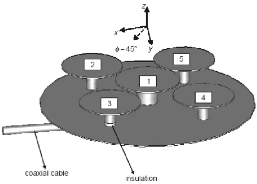
Fig. 1.1. Geometry of a 2-D pattern reconfigurable antenna based on Yagi-Uda antennas. array. By periodically switching those fixed beam patterns, the whole area can be scanned, but the main beam of the antenna pattern cannot focus on the direction of the arrival signal to continuously enhance the receiving signal. In contrast, adaptive array antennas can switch its main beam to the direction of the arrival signal smartly by combining and analyzing the collecting information of the arrival signal. Then, they can fix their main beam at the desired signal until the desired signal moves or stops. Apparently, adaptive antenna systems are the better design consideration to solve the interference and multi-path problems in wireless communication environments.
For utilizing the limited spectrum efficiently, lots of pattern diversity antennas have been proposed [2]-[20]. They are good candidates to reduce the interference caused by multi-path situations and other devices and increase the power efficiency due to adaptive beam-forming patterns and high directional gain. Many of pattern reconfigurable antennas are developed from the Yagi-Uda antenna design [1]-[14]. In a Yagi-Uda antenna, if the length of the parasitic element is shorter than that of the active element, it will have a pulling pattern in the direction from the active element to the shorter parasitic element. Contrarily, if the length of the parasitic element is longer than that of the active element, it will have a pushing pattern in the direction from the longer parasitic element to the active element. Consequently, by arranging parasitic elements with different
4
Fig. 1.2. Geometry of a 3-D pattern reconfigurable antenna based on Yagi-Uda antennas.
Fig. 1.3. Geometry of a 3-D pattern reconfigurable antenna by changing feeding locations
lengths around the active elements, various patterns can be achieved. Furthermore, switches can be loaded on each parasitic element to change the length of each parasitic element easily and electronically [12]-[13]. In [2]-[3], a feeding monopole antenna is positioned between two parasitic elements with two switches on each one, as shown in Fig. 1.1. By controlling the two switches on each element at the same time, an element which is longer or shorter than a feeding monopole is easily achieved. By the combinations of the length variations of parasitic elements, three different patterns can be accomplished. The above one is a 2-D structure, and a 3-D structure is introduced in [4]-[6]. As shown in Fig. 1.2, the parasitic elements can be switched to open-circuit to the ground plane to from a director. Increasing the number of parasitic elements in each
5
Fig. 1.4. Geometry of a 3-D pattern reconfigurable antenna with circle arrangement of parasitic elements.
Fig. 1.5. A pattern diversity antenna by changing the induced current distribution on parasitic elements.
direction can enhance the directivity of the antennas, and stuffing substrate within the area where active and parasitic elements are located can reduce the total size of the proposed antenna [7].
Moreover, the cylinder rod monopole with disc plates can help reducing the height of the proposed antenna. In [8]-[9], changing the feeding antenna is a good way to switch patterns by using other antennas as parasitic elements, as shown in Fig. 1.3. Some
6
configurations of the parasitic elements are arranged in the shape of circle [10]-[12] to form more directional patterns, as shown in Fig. 1.4. In addition to changing length of parasitic elements, changing the induced current distribution on parasitic elements is also capable of switching patterns [12]-[14]. As shown in Fig. 1.5, using switches with three poles to change a parasitic element to be open-circuit, short-circuit or loaded causes variations of current distribution to switch patterns.
In the above mention to pattern diversity antennas, they operate only at single frequency band. Those single-band operations cannot be satisfied by users nowadays. In this thesis, we proposed three novel dual-band pattern diversity antennas. These antennas evolve from the right angle corner reflector antenna with combinations of the frequency selective surface (FSS) structures. Each frequency selective surface on the wall can be controlled by one switch. A dual-band feeding antenna is located at the center of the corner reflector antenna. The first proposed dual-band pattern diversity antenna consists of two-layer FSS walls that the four inner walls at four directions respectively are for higher frequency and the four outer walls at four directions respectively are for lower frequency. Eight switches are enough to obtain the pattern diversity. Basically, the patterns that we switch are the omni-directional pattern and the directional pattern caused by the corner reflectors. The second dual-band pattern diversity antenna is a progression from the first one. Only one-layer walls are needed to keep dual-band operation. Its size is much smaller than the first proposed antenna‘s size. There are two FSS structures printed on each wall, which are for higher frequency and for lower frequency, respectively. Besides, fewer switches are needed: only four switches are enough for using in dual bands. At the end, the third dual-band pattern diversity antenna is proposed. In the second antenna, two FSS structures are used to operate at dual bands, but only one FSS structures are needed in the third proposed antenna. Its structure is very simple to fabricate. The results of the third antenna are almost the same as the results of the second one. Similarly, only four switches are required here. All of the proposed antennas feature beam tilting property caused by the ground under the feeding antennas and reflecting walls. This property can reduce the co-channel interference. Therefore, they are greatly suitable for modern base station antenna applications.
7
Chapter 2 T
HEORY OF
T
HEORY OF
C
ORNER
R
EFLECTOR
A
NTENNA AND
F
REQUENCY
S
ELECTIVE
S
URFACE
2-1 C
ORNERR
EFLECTORA
NTENNAFig. 2.1. The configuration of a corner reflector antenna.
Based on the content in [15], corner reflector antennas are a good candidate to obtain a good gain and directivity in our antenna design. As shown in Fig. 2.1, a half-wavelength dipole is in the area with two metal plates which form a corner with particular angle. A corner reflector antenna with 90o angle is the most practical one. The corner reflector antenna can be analyzed by the image theory and the array principle, as shown in Fig. 2.2. After analyzing, we can find that the pattern shape, gain, and feed point impedance will all be a function of the spacing between the feed point and the cor ner, s. A good directivity can be achieved if 0.25λ ≤ s ≤ 0.7λ when the metal plates are of infinite extent, but the input impedance of a dipole feed will be around 125Ω which does not match to the usual port impedance, 50Ω. As shown in Fig. 2.3, the best spacing, s, is 0.5λ.
8
Fig. 2.2. The corner reflector with images shown and how they account for reflections.
Fig. 2.3. Principal plane patterns, |AF|, for a right angle corner reflector.
Therefore, we have to find a balance condition between good directivity and well-matching input impedance.
In real world, infinite metal plates are impossible to fabricate. Therefore, making the metal plates finite is necessary. By ray tracing, that the length of the metal plate of L=2s is an acceptable dimension in corner reflector antenna design to keep the directivity but with a broader main beam. The height of the metal plate, H, is suitable to use from 1.2 to 1.5 times the length of the feed element to minimize the direct radiation by the feed into the back region of the metal plates.
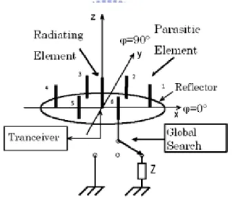
There are some corner reflector antennas proposed [16]-[20]. In Fig. 2.4, a three dimensional corner reflector antenna is introduced [16]. With the conducting plane under
9
Fig. 2.4. Geometry of a three-dimensional corner reflector antenna.
Fig. 2.5. Geometry of a triple corner reflector antenna.
the feeding element, the main beam will tilt and become narrower. In [18], a triple corner reflector antenna can narrow the main beam by two more corners, as shown in Fig. 2.5. Besides, using a cylindrical corner in the corner reflector antenna can increase the maximum gain because more image sources with constructive interference can be produced in Fig. 2.6[19]. Finally, a switching corner reflector antenna has been proposed [20]. As shown in Fig. 2.7, by controlling the lengths of the parasitic elements on the
10
Fig. 2.6. Geometry of a corner reflector antenna with the cylindrical corner.
Fig. 2.7. Geometry of a pattern reconfigurable antenna evolved from Yagi-Uda antennas and corner reflector antennas.
reflecting walls to reflect or to pull the antenna patterns, this corner reflector antenna can switch its main beam in four directions. These ideas are similar to the antenna designs we proposed in this thesis.
11
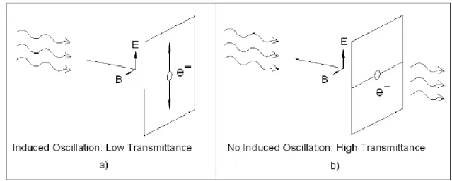
2-2 F
REQUENCYS
ELECTIVES
URFACEFig. 2.8. (a) An electron in filter plane undergoes oscillations driven by source wave. (b) An electron constrained to move along wire cannot undergo oscillations.
Frequency selective surface (FSS) is any surface construction designed as a ‗filter‘ for plane waves. It evolves from Radar Cross Section (RCS) with angular/frequency dependence. It has band pass/band stop behavior just like a conventional filter. Basically, it is a periodic structure in 2-D, typically, with narrow frequency bandwidth [21]. The operating principle of the FSS can be found in [22]. As shown in Fig. 2.8(a), a vertically polarized plane wave incident from the left side which strikes a metal plane at normal incidence. We can imagine what happens to a single electron located in the metal plane when the wave strikes the filter. Because the plane is orthogonal to the moving direction of the incident waves, the electronic field of the source lies in the plane. This electronic field exerts a force on the electron and causes it to oscillate if the condition is appropriate for oscillation. A portion of the energy from the incident waves must be converted into kinetic energy in order for the electron to remain in the oscillating state. To preserve conservation of energy, only a fraction of the incident power will be transmitted and the rest is absorbed by the electron. Then, the absorbed energy will be re-radiated from the oscillating electron. This re-radiated field cancels the electronic field at the backside of the FSS structure, and the FSS structure reflects the field back. If all of the energy from the wave is transferred to electrons in the metal or the backside fields are cancelled, then the transmittance through the filter will be zero. Next, now imagine a different situation.
12
Fig. 2.9. Different shapes of the FSS structures.
Think about that we have a line which lies in the metal plane but it also orthogonal to the E-field of the incident plane wave, as shown in Fig. 2.8(b). If an electron is limited to move along this wire, it will not be able to absorb kinetic energy from the incident wave because it is not allowed to accelerate in the direction that the force is exerted. In this case, the electron is effectively invisible to the incoming wave which will be fully transmitted.
Based on the theory of the FSS structure, numerous FSS structures are proposed in Fig. 2.9 [21]. Based on the shapes, sizes, loads and spacing between each element, we can determine the operating frequencies. Then, according to the orientation of each element, the dependence on polarization can be decided. Besides, recently, some dual-band FSS structures are proposed by implemented multiple resonant circuits [23]-[24].
13
Chapter 3 D
UAL
-B
AND
P
ATTERN
R
ECONFIGURABLE
A
NTENNA WITH
T
WO
-L
AYER
W
ALLS
3-1 A
NTENNAC
ONFIGURATION y x z S1b S2a S3a S4a S1a S2b S4b S3b Ground plane y x z y x z S1b S2a S3a S4a S1a S2b S4b S3b Ground planeFig. 3.1. Configuration of the proposed dual-band pattern reconfigurable antenna. Based on theories of the corner reflector antenna and the frequency selective surface, we combined them together to form a new dual-band pattern reconfigurable antenna. As shown in Fig. 3.1, a band pattern reconfigurable antenna comprises a center dual-band feeding antenna, four small-size rectangular plates at the inner sidewalls, four large-size rectangular plates at the outer sidewalls and a finite ground plate. The inner and outer sidewalls consist of switching FSS structures printed on the FR4 substrate with thickness of 0.8 mm. The inner walls can control patterns at higher frequencies, 5.25 GHz, while the outer walls can control patterns at lower frequencies, 2.45 GHz. Their properties of transmission and reflection are controlled by the switch states at the center of each wall. The switches are located between the center point of a metal control line and a ground. At one of the switch states, the FSS wall acts as a reflector which can block the electromagnetic waves at operating frequencies whereas at the other switch state, it becomes transparent to the electromagnetic waves at operating frequencies. When a
14
switch is passable, the center point of a metal control line and a ground plate are connected while when it is impassible, they are separated. In Fig. 3.1, S1a~S4a and S1b~S4b
are names of the switches located at the outer walls and the inner walls, respectively. According to the combinations of the switches at the inner and outer sidewalls, various patterns can be achieved at two frequency bands.
Based on the theory of the corner reflector antenna, the spacing between a reflecting wall and a feeding antenna is 0.5 wavelength. Therefore, the size of the ground plate is determined by the lower operating frequency, 2.45 GHz. The ground plate is fabricated on the FR4 substrate, whose thickness is 0.8 mm and whose dielectric constant is 4.4, with dimension of 140 mm × 140 mm.
The driving element, which is a dual-band antenna, is located at the center of the ground plate. It is designed for 2.45 GHz and 5.25 GHz. This antenna, which is perpendicular to the ground plate, is printed on the both side of the FR4 substrate with dimension of 40 mm × 30 mm × 0.8 mm. In addition, the matching microstrip line for the feeding antenna is made on the other of the substrate of the ground.
Besides, the associated circuitry of the switch, such as bias lines and RF chokes, can be fabricated on the backside of the ground plate to prevent the on-going electromagnetic waves from the unwanted influence by them because they are not showing in the path of electromagnetic waves.
According to the corner reflector antenna, the best spacing to get the best forward gain between the reflector wall and the feeding element is 0.5 wavelength therefore the spacing of the inner sidewall and the feeding antenna is 30 mm and that of the outer sidewall and the feeding antenna is 60 mm.
15
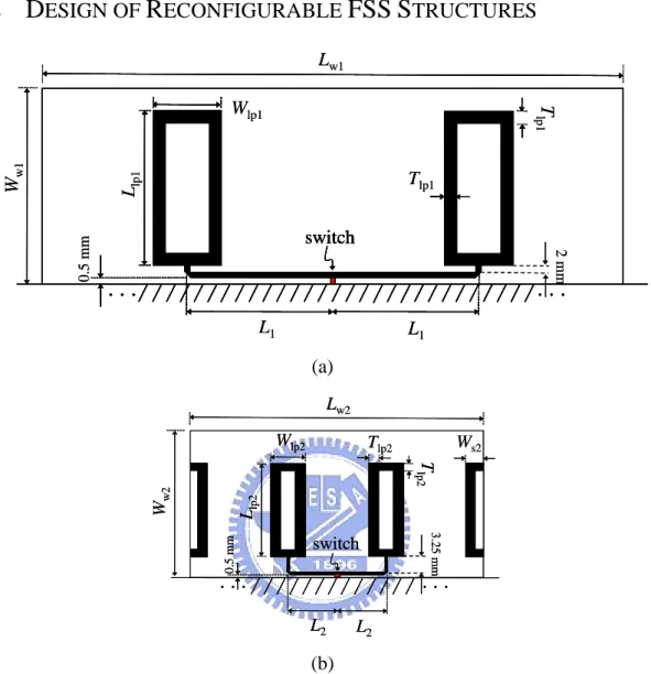
3-2 D
ESIGN OFR
ECONFIGURABLEFSS
S
TRUCTURESW w1 ‧‧‧ ‧‧‧ switch Lw1 Llp1 Wlp1 Tlp1 T lp1 0 .5 m m L1 L1 2 m m W w1 ‧‧‧ ‧‧‧ switch ‧‧‧ ‧‧‧ ‧‧‧ ‧‧‧ ‧‧‧ ‧‧‧ ‧‧‧ ‧‧‧ ‧‧‧ ‧‧‧ switch switch Lw1 Llp1 Wlp1 Tlp1 T lp1 0 .5 m m L1 L1 2 m m (a) ‧‧‧ ‧‧‧ switch Lw2 W w2 Ws2 Llp2 Tlp2 T lp2 0 .5 m m 3 .2 5 m m Wlp2 L2 L2 ‧‧‧ ‧‧‧ ‧‧‧ ‧‧‧ switch Lw2 W w2 Ws2 Llp2 Tlp2 T lp2 0 .5 m m 3 .2 5 m m Wlp2 L2 L2 (b)
Fig. 3.2. Geometries of the dual-band FSS structures (a) the outer walls (b) the inner walls
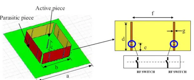
In our proposed antenna, we focus on the vertical polarization. Referring to Chapter 2.2, among lots of FSS structures, we choose a rectangular loop to be our design of the FSS structure because it is easier to design the FSS for particular polarization. Therefore, we have to make the vertical arms of the rectangular loops longer than the horizontal arms of it to make this FSS structure only respond to vertical polarization.
The geometries of the dual-band FSS structures are shown in Fig. 3.2. These walls are perpendicular to the ground plate. They consist of two rectangular loops and a metal control line connecting two rectangular loops together. In Fig. 3.2(a), the FSS structure with (Lw1, Ww1) = (120 mm, 40 mm) is designed for operating at 2.45 GHz. Two parallel
16
rectangular loops are built to form the FSS structures. The circumference of a rectangular loop to be a FSS is one wavelength. Llp1 and Wlp1 are the length and the width of the
rectangular loop, and they are 32 mm and 14 mm, respectively. The thickness of the rectangular loop, Tlp1, is 2.5 mm. The distance between the two parallel rectangular loops
is about half wavelength of the operating frequency. Therefore, the length of the printed metal control line connecting two rectangular loops is about half wavelength too. L1 is the
horizontal distance between the center point of the metal line and the center point of the rectangular loop with length of 30 mm. The gap between the metal line and the ground plate is 0.5 mm, and it is a location for mounting a switch. In Fig. 3.2(b), the definitions of the parameters of the FSS structures for 5.25 GHz are the same as that for 2.45 GHz except for Wside2. Its parameters, (Lw2, Ww2, Llp2, Wlp2, Tlp2, L2), are (60 mm, 30 mm, 19
mm, 7 mm,2 mm,10 mm). As shown in Fig. 3.2(b), we can see that the configuration of the inner sidewalls is different from that of the outer sidewalls. We add two half rectangular loops at each side of the wall with the same length as the center rectangular loops and with Ws2 = 3.5 mm. They can form extra loops with other two nearby inner
walls in the configuration of the proposed antenna to increase the directivity of the patterns at 5.25 GHz. We will discuss its function later.
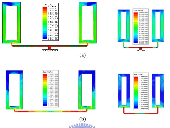
The FSS structures are controlled by the switch states and the metal transmission line. First, we define that when a switch is passable, which means that the center point of the metal transmission line and the ground plane are connected, we call this switch state ―on‖; otherwise, we call it ―off‖. Now we start to discuss about the working mechanism of the switching FSS structures. At the beginning, we can see the current distribution at 2.45 GHz when the FSS structures without the control transmission line. When the FSS structure is hit by vertically polarized electromagnetic waves, it will resonate at the operating frequency when its circumference is about one wavelength of the operating frequency which is 2.45 GHz in this case. Due to resonance, they will be excited strong current distribution which has strong current at the center of the vertical arms and current null at the center of the horizontal arms, as shown in Fig. 3.3(a). Then, these current re-radiate electromagnetic waves, which cancel the on-going electromagnetic fields at the backside of the wall and enhance the fields in front of the walls if the spacing between
17
(a)
(b)
(c)
Fig. 3.3. Current distributions of the FSS structures at 2.45 GHz on (a) two rectangular loops. (b) a switching FSS when the switch is on. (c) a switching FSS when the switch is off.
the feeding antenna and the reflector plate is adequate. As a result, it can reflect the on-going waves.
18
(a)
(b)
(c)
Fig. 3.4. Current distributions of the FSS structures at 5.25 GHz on (a) two rectangular loops. (b) a switchable FSS when the switch is on. (c) a switchable FSS when the switch is off.
Next, we consider a switching FSS with a metal control line. When the switch is ―on‖, the center point of the control line is short-circuit. Through the quarter-wave control line from the center point to the end point, open-circuit shows at the end point according to the transmission line theory [25]. As shown in Fig. 3.3(b), the resonant current
19 PBC PBC PEC Port 2 Port 1 FSS PBC PBC PEC Port 2 Port 1 FSS
Fig. 3.5. The simulation model for designing FSS structures.
distribution on the rectangular loops will be kept the same as Fig. 3.3(a). As a result, this switching FSS structure reflects the incident waves just like the FSS structure made up of rectangular loops.
On the other hand, when the switch is ―off‖, the center point of the control line is separate from the ground plate. Based on the theory of symmetry, current null, which is similar to open-circuit, appears at the center point of the control line. Due to the quarter-wavelength control line, short-circuit shows up at both ends of the control line. Therefore, the resonant current distribution on the rectangular loops is destroyed. In Fig. 3.3(c), we can see that the current level is weaker than that of the above condition, even though the current distribution looks similar. Because of the weaker current level, the re-radiated electromagnetic fields by those current are too small to reflecting incoming waves. As a result, this FSS structure looks transparent to incoming waves. Incoming waves can pass through the walls easily. Based on above discussion, a switching FSS at 2.45 GHz is completed. The discussion of a switching FSS at 5.25 GHz is the same as that at 2.45 GHz. Its current distribution at 5.25 GHz is shown in Fig. 3.4.
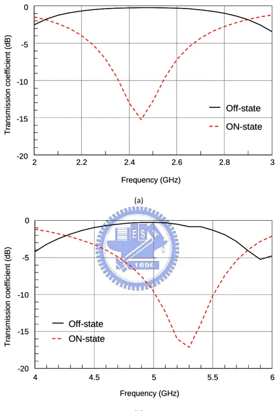
20 2 2.2 2.4 2.6 2.8 3 Frequency (GHz) -20 -15 -10 -5 0 Off-state ON-state T ra n smi ssi o n c o e ff ici e n t (dB ) 2 2.2 2.4 2.6 2.8 3 Frequency (GHz) -20 -15 -10 -5 0 Off-state ON-state T ra n smi ssi o n c o e ff ici e n t (dB ) (a) 4 4.5 5 5.5 6 Frequency (GHz) -20 -15 -10 -5 0 Off-state ON-state T ra n smi ssi o n c o e ff ici e n t (dB ) 4 4.5 5 5.5 6 Frequency (GHz) -20 -15 -10 -5 0 Off-state ON-state T ra n smi ssi o n c o e ff ici e n t (dB ) (b)
Fig. 3.6. The simulated transmission coefficients at (a) 2.45 GHz (b) 5.25 GHz when the switches are in ON-state or Off-state.
The simulation method is shown in Fig. 3.5. The periodic boundary condition (PBC) is set at left and right sides of the wall to simulate the periodic condition of FSS. A
21
(a)
(b)
Fig. 3.7. The simulated current distributions in the dual-band pattern reconfigurable reflector antenna at 2.45 GHz (large loops) and 5.25 GHz (small loops) in (a) ON-state. (b) Off-state.
perfect conductor (PEC) is assign to the plane under the wall. Then, two ports with vertical polarization are set at the upper and bottom plane to excite vertically polarized electromagnetic waves which is incident to FSS structures. The distance between one of the ports and the FSS structures is longer than quarter wavelength to make sure that the boundary condition at ports does not affect the proposed FSS structures in our simulations. In the beginning, we define that ‗ON-state‘ is that the FSS walls can reflect the vertically polarized incident waves while ‗Off-state‘ is that the FSS walls is transparent to the vertically polarized incident waves. The simulated transmission coefficients (S21) are shown as Fig. 3.6. We can see that as the switches for 2.45 GHz and
5.25 GHz are on, the transmission coefficients at both frequencies are lower than -10 dB, which are -15.27 dB and -16.58 dB, respectively. They are good enough to prevent incoming waves from passing through the walls. On the other hand, when the switches are off, the transmission coefficients are higher than 1 dB, which are 0.208 dB and -0.684 dB, respectively. That means that all of incoming waves pass through the walls. The simulated current density distributions in ON-state and Off-state at both frequencies,
22
2.45 GHz and 5.25 GHz, are shown in Fig. 3.7. Vertically polarized incident waves are used to be a source. The results are similar to what we mentioned above. Due to the coupling effects between the rectangular loops and the transmission line, the open-circuit conditions do not really occur at the connecting points, as shown in Fig. 3.7(a). However, the resonances still remain on both structures. On the other hand, in Fig. 3.7(b), the current distribution on the rectangular loops in Off-state is weaker than that in ON-state.
After we completed our design of the switching FSS walls, a dual-band pattern reconfigurable reflector antenna can be fabricated by those walls operating at 2.45 GHz and 5.25 GHz.
23
3-3 D
ESIGN OF THED
UAL-B
ANDP
ATTERNR
ECONFIGURABLER
EFLECTORA
NTENNA WITHT
WO-L
AYERW
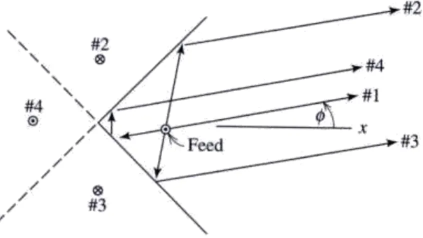
ALLSIn this section, we will talk about the functions of the two more half rectangular loops on the inner wall, the interactions between the inner walls and the feeding antenna, and design of the feeding antenna. Here, we define that ―Case 1‖ represents that all of the inner and outer switches are in off-state, which means that all of the walls are transparent to vertically polarized electromagnetic waves, and that ―Case 2‖ represents that the switches, S1a, S4a on the outer walls and S1b, S4b on the inner walls, are in on-state,
which means that a corner reflector antenna is formed and its directivity points to = 225oat 2.45 GHz and 5.25 GHz.
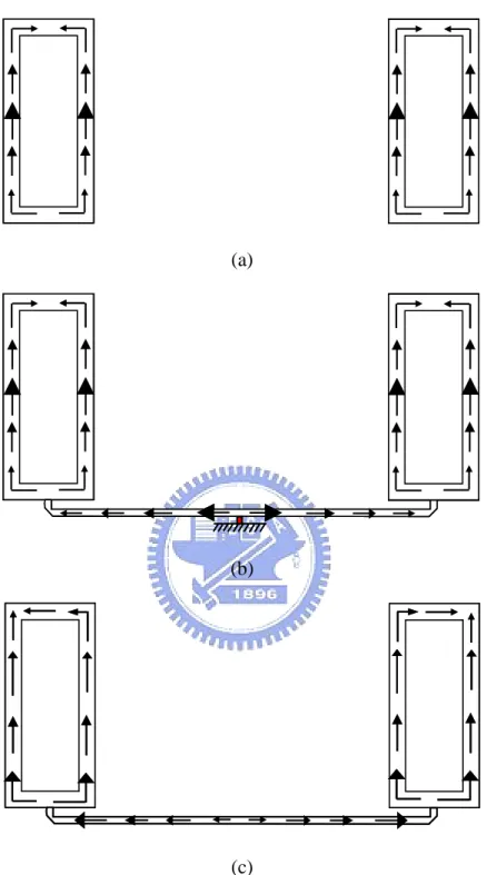
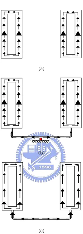
3-3-1 Functions of the two more half rectangular loops printed on the inner
wall
At the very beginning, there are only the center two rectangular loops and a metal control line printed on the FR4 substrate of the inner walls. Its parameters, (Llp2, Wlp2, Tlp2,
L2), are (10.5 mm, 6 mm, 2 mm,15.25 mm). When we use it to be the inner FSS wall to
reflect electromagnetic waves at 5.25 GHz, the simulated pattern of Case 2 is shown in Fig. 3.7. The dash line here represents the above simulated pattern. The directivity and the front-to-back ratio are not good enough for usage. The back lobe we define here is the direction at the angle between the maximum of the main lobe and the z axis at the other side of the z axis. To solve this problem, we add four corner loops to our proposed antenna configuration by implementing two half rectangular loops at both side of each inner wall. Due to increment of those corner loops, we have to reassign the positions of the center rectangular loops to form a periodic structure with a new period. When the switch is in on-state, the center rectangular loops and the corner loops form a good FSS structure to reflect waves at 5.25 GHz, and in Case 2, the corner rings can help to reflect the leak waves at the corner to increase the front-to-back ratio, as shown in Fig. 3.8. The solid line represents the simulated pattern of the modified antenna configuration, and it shows that the back lobe is much smaller than the previous one so its front-to-back ratio has been improved. On the other hand, when the switch is in off-state, the period formed by the corner loops is not adequate for FSS structures operating at 5.25 GHz. The
24 -20 -17 -14 -11 -8 -5 -2 1 4 7 10 -20 -17 -14 -11 -8 -5 -2 1 4 7 10 0 30 60 90 120 150 180 210 240 270 300 330
With corner loops Without corner loops
-20 -17 -14 -11 -8 -5 -2 1 4 7 10 -20 -17 -14 -11 -8 -5 -2 1 4 7 10 0 30 60 90 120 150 180 210 240 270 300 330
With corner loops Without corner loops
Fig. 3.8. The comparison of the patterns in= 45o plane in case 2 at 5.25 GHz between the FSS wall for 5.25 GHz with corner rings and without corner loops.
walls look transparent to the incident waves just like the wall without corner loops. Consequently, the new proposed antenna can work well as a pattern reconfigurable antenna.
3-3-2 Interactions between the inner walls and the feeding antenna
In Fig. 3.9, the solid line shows the pattern at 2.45 GHz when only the outer walls work as a corner reflector while the dash line represents the pattern at 5.25 GHz when both inner and outer walls work as corner reflectors. We can see that the maximum gain of the solid line is smaller than that of the dash line. Based on the theory of Yagi-Uda antennas [15], a parasitic element which is shorter than a feeding element and is located in front of a feeding element act as a director to pull its radiation patterns out. Therefore, when the switch on the inner wall is in off-state, each side of the center rectangular loops with half of the control line forms a director at 2.45 GHz. As a result, the radiation pattern at 2.45 GHz is pulled out to spread at four directions to reduce the maximum gain of the main beam. Nevertheless, if the switch on the inner wall is in on-state, this current
25 -20 -17 -14 -11 -8 -5 -2 1 4 7 10 -20 -17 -14 -11 -8 -5 -2 1 4 7 10 0 30 60 90 120 150 180 210 240 270 300 330 S1a、S4a: on ; S1b、S4b: off S1a、S4a: on ; S1b、S4b: on -20 -17 -14 -11 -8 -5 -2 1 4 7 10 -20 -17 -14 -11 -8 -5 -2 1 4 7 10 0 30 60 90 120 150 180 210 240 270 300 330 S1a、S4a: on ; S1b、S4b: off S1a、S4a: on ; S1b、S4b: on
Fig. 3.9. The comparison of the patterns in = 45o plane in case 2 at 2.45 GHz between the switches, S1b、S4b, in off-state and on-state.
distribution of the director is destroyed by connecting ground so it does not affect the pattern at 2.45 GHz. In conclusion, when we use this dual-band pattern reconfigurable reflector antenna, we have to make the switches in the same direction be in the same state, regardless of mounting on the inner or outer walls. Besides, we can just use one switch to control the inner and outer walls in the same direction at the same time to reduce the number of the switches for decreasing the cost.
3-3-3 Design of the feeding antenna
In this antenna design, we have to find an antenna which can have a good match in both cases. It is hard to design this kind of antenna because the electromagnetic field excited by an antenna in different cases is quite different from each other. Therefore, antenna design becomes one of the important designs in the proposed antenna module.
A proposed antenna is shown in Fig. 3.10. It consists of two trident structures that that the front and lower one is for 5.25 GHz and the combination of both trident structures is for 2.45 GHz. The parameters for the front trident structure, (H1, B1, A1, D1), are (2 mm, 3
26 W3 L 3 H1 H2 D1 D2 H3 A 1 A 3 A2 B3 B2 B 1 0.8 mm W3 L 3 H1 H2 D1 D2 H3 A 1 A 3 A2 B3 B2 B 1 W3 L 3 H1 H2 D1 D2 H3 A 1 A 3 A2 B3 B2 B 1 W3 L 3 H1 H2 D1 D2 H3 A 1 A 3 A2 B3 B2 B 1 W3 L 3 H1 H2 D1 D2 H3 A 1 A 3 A2 B3 B2 B 1 0.8 mm
Fig. 3.10. The dual-band feeding antenna with two trident structures.
mm, 7 mm, 3.25 mm), and the parameters for the back trident structure, (H2, A2, B2, D2,
A3, B3, H3), are 8 mm, 13 mm, 2mm, 5.25 mm, 21mm, 1.5 mm and 2 mm, respectively.
By tuning the values of A1 and H3 can change the amount of the coupling. To excite the higher frequency, we feed into the front trident structure directly by a mircostrip line printed on the other side of the ground substrate. Its center arm is about quarter wavelength of 5.25 GHz. For the excitement of the lower frequency, we use the coupling effect between two trident structures. The total length of the center arm in the lower trident structure and the center arm in the higher trident structure is about quarter wavelength of 2.45 GHz. Besides, the arms at both sides can increase amounts of the coupling and increase the impedance bandwidth, especially at higher frequency band. The simulated and measured results are shown in Fig. 3.11. We can see that the impedance bandwidth which is lower than -10 dB at higher frequency band is from 3.12 GHz to 5.75 GHz and that at lower frequency is from 2.23 GHz to 2.64 GHz. The measured result is quiet similar to the simulated result at lower frequency band. The problems caused by fabrication may make the differences at higher frequency band. Basically, the range which is lower than -10 dB is almost the same as the simulated result at higher frequency band.
27 Ret u rn l o ss (d B ) 1 1.5 2 2.5 3 3.5 4 4.5 5 5.5 6 Frequency (GHz) -40 -35 -30 -25 -20 -15 -10 -5 0 simulation measurement Ret u rn l o ss (d B ) 1 1.5 2 2.5 3 3.5 4 4.5 5 5.5 6 Frequency (GHz) -40 -35 -30 -25 -20 -15 -10 -5 0 simulation measurement 1 1.5 2 2.5 3 3.5 4 4.5 5 5.5 6 Frequency (GHz) -40 -35 -30 -25 -20 -15 -10 -5 0 simulation measurement
28
3-4 M
EASUREMENTR
ESULTSFig. 3.12. The photo of the complete dual-band pattern reconfigurable reflector antenna. The photograph of the complete dual-band pattern diversity antenna is shown in Fig. 3.12. Various patterns can be obtained by the combinations of the switch states. In real applications, the omni-directional and directional patterns are more important than others. We use the directional patterns to detect where the signal comes from and then focus on the direction of the signal to increase the receiving power of the signal and reduce the noise and the multi-path effects. Besides, we can use the omni-directional pattern to transmit the signals to each devices to save the transmission time. Consequently, we only focus on the results of the cases with the omni-directional and directional pattern, respectively. The definitions of both cases and the measured and simulated results at both cases are listed in TABLE II
The measurement results of return loss of case 1 (omni-direction) and the case 2 (direction) are shown in Fig. 11. In Case 1, it can be seen that the -10 dB bandwidth is from 2.39GHz to 2.52 GHz in lower frequency region and from 5.25 GHz to 5.54 GHz in higher frequency region. In applications, the bandwidths of both the frequency regions
29
are enough. In Case 2, the -10 dB bandwidth is from 2.32 GHz to 2.5 GHz in lower frequency region and from 5.12 GHz to 5.48 GHz. Both of them accord with the specifications in these bands. Therefore, this dual-band coupling feeding antenna is a good candidate for use to reduce the complex matching circuits.
The measured patterns of Case 2, a directional case, and Case 1, an omni-directional case, at 2.45 GHz and 5.25 GHz are shown in Fig. 3.13and Fig. 3.14, respectively In Fig. 3.13(a), a directional pattern can be seen whose peak gain of 5.85 dBi at 2.45 GHz is
TABLE II
THE DEFINITIONS OF THE TWO FUNDAMENTAL CASES AND THE SIMULATED AND MEASURED RESULTS OF THE DUAL-BAND PATTERN RECONFIGURABLE ANTENNA WITH
TWO-LAYER WALLS
Switch Case1 Case2
S1a ,S1b Off On S2a ,S2b Off Off S3a ,S3b Off Off S4a ,S4b Off On Simulated peak gain direction 2.45GHz Omni = -53o = 225o 5.25GHz Omnilike = -60o = 225o Simulated peak gain (dBi) 2.45GHz 0.50 6.17 5.25GHz 5.73 9.24 Measured peak gain direction 2.45 GHz Omni = -73o = 225o 5.25 GHz Omnilike = -63o = 225o Measured peak gain (dBi) 2.45 GHz 0.23 5.85 5.25 GHz 1.13 9.18
30 -20 -17 -14 -11 -8 -5 -2 1 4 7 10 -20 -17 -14 -11 -8 -5 -2 1 4 7 10 0 30 60 90 120 150 180 210 240 270 300 330 -20 -17 -14 -11 -8 -5 -2 1 4 7 10 -20 -17 -14 -11 -8 -5 -2 1 4 7 10 0 30 60 90 120 150 180 210 240 270 300 330 -20 -17 -14 -11 -8 -5 -2 1 4 7 10 -20 -17 -14 -11 -8 -5 -2 1 4 7 10 0 30 60 90 120 150 180 210 240 270 300 330 -20 -17 -14 -11 -8 -5 -2 1 4 7 10 -20 -17 -14 -11 -8 -5 -2 1 4 7 10 0 30 60 90 120 150 180 210 240 270 300 330 = 45o-plane = 45o-plane -20 -17 -14 -11 -8 -5 -2 1 4 7 10 -20 -17 -14 -11 -8 -5 -2 1 4 7 10 0 30 60 90 120 150 180 210 240 270 300 330 -20 -17 -14 -11 -8 -5 -2 1 4 7 10 -20 -17 -14 -11 -8 -5 -2 1 4 7 10 0 30 60 90 120 150 180 210 240 270 300 330 -20 -17 -14 -11 -8 -5 -2 1 4 7 10 -20 -17 -14 -11 -8 -5 -2 1 4 7 10 0 30 60 90 120 150 180 210 240 270 300 330 -20 -17 -14 -11 -8 -5 -2 1 4 7 10 -20 -17 -14 -11 -8 -5 -2 1 4 7 10 0 30 60 90 120 150 180 210 240 270 300 330 = 45o-plane = 45o-plane (a) (b)
Fig. 3.13. The measured and simulated patterns of Case 2 at (a) 2.45 GHz (b) 5.25 GHz. measured at (θ = -73o, = 225o) with the side lobe level of 8.9 dB, while the peak gain of 9.18 dBi at 5.25 GHz is measured at (θ = -63o, = 225o) with the side lobe level of 13.5 dB, as shown in Fig. 3.13(b). In addition, due to the beam tilting properties caused by the ground plane, the radiation patterns on = 45o-plane are measured too. Apparently, the directional property toward where the switch states are off is good for use at both frequencies. The measured radiation patterns at = 45o-plane coincide with the simulated ones at both frequencies. For Case 1, as shown in Fig. 3.14(a), the measured patterns at 2.45 GHz agree well with the simulated results in three different planes, = 45o-, yz- and
measurement simulation measurement simulation
31 -20 -17 -14 -11 -8 -5 -2 1 4 7 10 -20 -17 -14 -11 -8 -5 -2 1 4 7 10 0 30 60 90 120 150 180 210 240 270 300 330 -20 -17 -14 -11 -8 -5 -2 1 4 7 10 -20 -17 -14 -11 -8 -5 -2 1 4 7 10 0 30 60 90 120 150 180 210 240 270 300 330 -20 -17 -14 -11 -8 -5 -2 1 4 7 10 -20 -17 -14 -11 -8 -5 -2 1 4 7 10 0 30 60 90 120 150 180 210 240 270 300 330 -20 -17 -14 -11 -8 -5 -2 1 4 7 10 -20 -17 -14 -11 -8 -5 -2 1 4 7 10 0 30 60 90 120 150 180 210 240 270 300 330 = 45o-plane = 45o-plane -20 -17 -14 -11 -8 -5 -2 1 4 7 10 -20 -17 -14 -11 -8 -5 -2 1 4 7 10 0 30 60 90 120 150 180 210 240 270 300 330 -20 -17 -14 -11 -8 -5 -2 1 4 7 10 -20 -17 -14 -11 -8 -5 -2 1 4 7 10 0 30 60 90 120 150 180 210 240 270 300 330 -20 -17 -14 -11 -8 -5 -2 1 4 7 10 -20 -17 -14 -11 -8 -5 -2 1 4 7 10 0 30 60 90 120 150 180 210 240 270 300 330 -20 -17 -14 -11 -8 -5 -2 1 4 7 10 -20 -17 -14 -11 -8 -5 -2 1 4 7 10 0 30 60 90 120 150 180 210 240 270 300 330 xz-plane xz-plane -20 -17 -14 -11 -8 -5 -2 1 4 7 10 -20 -17 -14 -11 -8 -5 -2 1 4 7 10 0 30 60 90 120 150 180 210 240 270 300 330 -20 -17 -14 -11 -8 -5 -2 1 4 7 10 -20 -17 -14 -11 -8 -5 -2 1 4 7 10 0 30 60 90 120 150 180 210 240 270 300 330 -20 -17 -14 -11 -8 -5 -2 1 4 7 10 -20 -17 -14 -11 -8 -5 -2 1 4 7 10 0 30 60 90 120 150 180 210 240 270 300 330 -20 -17 -14 -11 -8 -5 -2 1 4 7 10 -20 -17 -14 -11 -8 -5 -2 1 4 7 10 0 30 60 90 120 150 180 210 240 270 300 330 yz-plane yz-plane (a) (b)
Fig. 3.14. The measured and simulated patterns of Case 1 at (a) 2.45 GHz (b) 5.25 GHz.
measurement simulation measurement simulation
32
xz-plane. The peak gain is about 0 dB due to the effect of the pulling directors acted by the inner FSS walls. In Fig. 3.14(b), at 5.25 GHz, the measured radiation patterns are similar to the simulated patterns in = 45o-, yz- and xz-plane, too. The maximum gain is 2.45 dB. At both frequencies, the variations of the patterns in = 45o-plane are less than 3dB so good omni-directional patterns are obtained. In addition, because of the beam tilting property, the maximum gains are located within -60o < θ < 60 o. From above, it shows that both omni-directional and directional pattern are provided by this antenna.
33
Chapter 4 D
UAL
-B
AND
P
ATTERN
R
ECONFIGURABLE
A
NTENNA WITH
S
INGLE
-L
AYER
W
ALLS
x
y
z
S
1S
4S
3S
2 Ground planeS
4x
y
z
x
y
z
S
1S
4S
3S
2 Ground planeS
4Fig. 4.1. The configuration of the proposed dual-band pattern reconfigurable antenna. The size of the above design is determined by the wavelength of the lower frequency. Due to mounting the FSS walls on the ground, its size is 140 mm × 140 mm × 0.8 mm. This size is a little larger in the application for mobile devices. Therefore, we have to make it smaller if we plan to use it in mobile devices.
4-1 A
NTENNAC
ONFIGURATIONThe antenna configuration of this antenna is similar to the above one. It is made of a center dual-band feeding antenna, four rectangular walls and a finite ground, as shown in Fig. 4.1. Each wall has two groups of rectangular loops, which can reflect the vertically polarized incident electromagnetic waves when they resonate. The operating frequencies here are 2.45 GHz and 5.25 GHz. The properties of transmission and reflection of the loops are controlled by switches, whose names are S1~S4, and horizontal and vertical
34
resonate by excitement from vertically polarized incident wave. Therefore, they can reflect the waves. On the other switch state, those loops are disabled from resonance to look invisible for the vertically polarized incident waves. Only one switch is needed for usage on each wall, and it can reduce the cost of fabrication. Every switch is located at the intersection of the two control lines and the ground plate at the backside of the substrate of the wall. When the switch is transmissive, the center point of the horizontal control line and the end point of the vertical control line connect to the ground plate to form a short-circuit condition at those points. Contrarily, those points are isolated from the ground plate to be in an open-circuit condition when the switch is not threaded through.
The ground size is determined by the spacing between the driving element and the reflecting wall because those walls are vertically mounted on the ground plate. The ground size is quite smaller than the ground of the first proposed antenna because shorter spacing and the length of the walls. With dimension of 30 mm × 30 mm × 0.8 mm, the ground plane is fabricated on FR4 substrate with relative permittivity of 4.4.
A dual-band antenna is located at the center of the ground plate and designed for 2.45 GHz and 5.25 GHz. This antenna, which is perpendicular to the ground plate, is printed on the both side of the FR4 substrate with dimension of 40 mm × 30 mm × 0.8 mm. In addition, the matching circuit for the feeding antenna is printed on the other side of the substrate of the ground.
Moreover, the associate circuits for the switches can be fabricated under the ground plane, just like the first antenna. Therefore, the advantage that those circuits do not affect the properties of the antenna can be kept in this antenna. Designing circuits becomes easier because we can build our circuits without considering the influences on the antenna.