國 立 交 通 大 學
電 子 工 程 學 系 電 子 研 究 所
碩 士 論 文
利用金屬薄膜與奈米碳管為場發射材料之
側向式場發射元件之研究
Study on the Lateral Field Emission Devices
Using the Metal Thin Films and Carbon Nanotubes
as the Emitter Materials
研 究 生:許 育 瑛
指導教授:鄭 晃 忠 博士
利用金屬薄膜與奈米碳管為場發射材料之
側向式場發射元件之研究
Study on the Lateral Field Emission Devices
Using the Metal Thin Films and Carbon Nanotubes
as the Emitter Materials
研 究 生:許育瑛 Student: Yu-Ying Hsu
指導教授:鄭晃忠 博士 Advisor: Dr. Huang-Chung Cheng
國
立 交 通 大 學
電子工程學系
電子研究所碩士班
碩士論文
A Thesis
Submitted to Department of Electronics Engineering & Institute of Electronics College of Electrical Engineering and Computer Engineering
National Chiao Tung University In Partial Fulfillment of the Requirements
for the Degree of Master in
Electronics Engineering 2008
Hsinchu, Taiwan, Republic of China
利用金屬薄膜與奈米碳管為場發射材料之側向
式場發射元件之研究
研究生:許育瑛 指導教授:鄭晃忠 博士
國立交通大學電子工程學系
電子研究所碩士班
摘
要
對於場發射元件而言,為改善場發射特性使其可應用在高效能元件上,降低元件的 操作電壓與增加場發射電流是非常必要的。此篇論文中,我們提出兩種側向式場發射元 件以達成上述目標。 第一種元件為金屬薄膜邊緣側向場發射器,此種結構可將發射器與收集器之間的距 離降至150奈米,因此可降低操作電壓,同時,此距離可藉由非晶質矽的厚度準確控制。 在元件製備完成之後,對元件進行氫氣或乙烯之後處理,使其進一步改善場發射特性。 對鈷薄膜邊緣場發射器而言,在經過乙烯處理之後,場發射特性有明顯改善,這是由於 處理後產生石墨層與碳化物,造成鈷表面的起伏遽增,因而增大了場發射增強因子,使 場發射電流達到10-7 安培的起始電壓可降至8伏特,相較之下,經過氫氣處理之後,其 起始電壓為12伏特,這是由於經氫氣處理後的表面起伏不如乙烯處理來得明顯;另一方 面,鈀薄膜邊緣場發射器在經過乙烯及氫氣個別處理之後,表面起伏無明顯改變,這是 由於鈀薄膜與底層的鎢膜表面能差異較大,底層的鎢膜不傾向露出表面,而經過乙烯處 理後,其起始電壓為25.5伏特,相較之下,經過氫氣後處理之後,場發射特性具有明顯 改善,這是由於鈀經過氫處理後產生PdHX,而PdHX的功函數較純Pd小,於是,此種利 用Pd為場發射極的側向式場發射元件可進一步將起始電壓降至6.5伏特。此外,基於奈米碳管的優異場發射特性,我們提出同平面式與階梯式兩種不同型態 的側向式場發射元件。對於同平面式的場發射元件而言,當發射器與收集器之間的距離 固定為2 μm時,其起始電壓為9伏特。為進一步改善場發射特性,我們提出另一種階梯 式的側向式場發射元件,利用收集器底下的氧化層厚度變化,使得碳管頂端更加接近收 集器以增強場發射電流,此種結構可將起始電壓進一步降至1.8伏特。 根據實驗的結果,奈米碳管的場發射特性較金屬薄膜為佳,即使金屬薄膜場發射器 可將收集器與發射器之間的距離縮得更短。
Study on the Lateral Field Emission Devices
Using the Metal Thin Films and Carbon
Nanotubes as the Emitter Materials
Student : Yu-Ying Hsu Advisor : Dr. Huang-Chung Cheng
Department of Electronics Engineering &
Institute of Electronics
National Chiao Tung University
Abstract
For the sake of improving field emission characteristics of field emission devices to apply on high performance devices, lower operation voltage, and higher field emission current are required in field emission devices. In this thesis, two kinds of lateral field emitters are proposed to accomplish such aims.
Thin film edge field emitters with small emitter-to-collector gap as small as 150 nm are proposed to reduce the operation voltage. The distance between emitter and collector is defined by the thickness of amorphous silicon and hence could be controlled precisely. After the devices are fabricated, the samples are treated by C2H4 and H2 individually to improve the
field emission characteristics further. The cobalt thin film edge field emitters treated with C2H4 gas could enhance field emission current by increasing the roughness of Co surface due
Co emitter, the turn-on voltage at an emission current of 100 nA could be reduced to 8 V after being treated with C2H4 gas. As compared with treated with C2H4, the improvement of field
emission characteristics of Co emitters treated with H2 was not so obvious due to less increase
of roughness and the turn-on voltage was 12 V. On the other hand, the change of roughness of the palladium field emitters treated with C2H4 and H2 gas was not apparent due to the large
difference of surface energy between Pd and under-layer, W. The turn-on voltage of Pd emitters treated with C2H4 was 25.5V. However, it could be reduced to 6.5 V after the Pd ones
being treated with H2 to form the PdHX which owns lower work function than pure Pd.
Additionally, two types of emission devices, co-planar and step-type ones, based on carbon nanotubes are proposed. The turn-on voltage of co-planar type lateral field emission devices with emitter-to-collector gap fixed at 2 μm is 9 V. On the other hand, step-type lateral field devices are also proposed to improve the field emission characteristics. In contrast to the co-planar ones, the distance between the tips of CNTs and collector could be shrunk by increasing the thickness of oxide under collector and hence could lower the operation voltage and enhance the field emission current. The turn-on voltage of step-type lateral field emission devices could be further reduced to 1.8 V.
According to the experimental results, the field emission characteristic of CNTs is better than the metal thin films even with a shorter emitter-to-collector distance.
誌謝
感謝國立交通大學所有曾經教導我的老師,特別感謝我的指導教授-鄭晃忠博士, 謝謝老師在論文上的指導,使得論文可以順利完成,並且感謝老師在生活中的幫忙與關 心,鼓勵我參加國外研討會拓展眼界,並在尋找工作時提供協助。 感謝林高照學長在論文上的指導,在實驗上給予方向與啟發,遇到困難時總是二話 不說給予協助,並且每週挪出時間幫我拍攝電子顯微鏡照片;感謝賴瑞霖學長在論文上 給予建議,以及謝謝已經畢業的柳耀星學長、陳俠威學長和林君翰學長在機台上的訓 練,還有總是關心與照顧我的張佩琪學姐與林心瑜學姐。 其次,要感謝交通大學奈米中心 (NFC) 和國家毫微米實驗室 (NDL) 提供完善的實 驗設備,尤其感謝奈米中心的技術人員-林聖欽先生、倪月珍小姐、范秀蘭小姐、徐綉 鑾小姐、陳悅婷小姐、彭兆光先生…等,在實驗設備及維護上給予最大協助,也感謝何 惟梅小姐、顏似妙小姐和簡秀芳小姐在行政方面的幫忙,以及奈米科技中心的鍾怡娟小 姐。 再來感謝 ED309b 實驗室所有的夥伴們,謝謝同組的張加聰學長在實驗上的幫忙, 互相加油打氣的李建穎,認真向學的魏英彰與蔡萬霖學弟,因為有你們的陪伴,做實驗 的時間變得有趣而不冗長;還有感謝一起努力奮鬥的同學們,義氣的李序恆、超有型的 林偉凱、常被迫陪我走回宿舍的涂仕煒以及熱心的劉政欽,共同奮鬥的日子裡,壓力常 常就在大家笑鬧中釋放了;感謝實驗室的阮全平學長、廖大傳學長、李逸哲學長與楊柏 宇學長在研究上的指導;感謝實驗室所有的學弟妹,在生活中的幫忙與陪伴,特別感謝 才女鄧茜云學妹與眼睛會笑的采綸,在生活裡的鼓勵與關心,聽我說話,給我支持。感 謝從前交大材料系的郭全雯同學與高珮玲同學,在實驗上提供協助。 感謝我的父親許志暉先生與母親楊惠貞女士,提供無虞的生活以及良好的學習機 會,並且在我煩惱時給予支持與鼓勵,感謝我的哥哥與妹妹在這段時間的陪伴,以及謝 謝我親愛的朋友以及曾經幫助我的人。 兩年是段不長也不短的時間,曾經煩惱的、挫敗的、感動的、快樂的,到這裡為止, 終須說再見,有點不捨卻滿懷感激,感謝那些曾經來去我生命的人們與故事,在名為青 春的軟緞上,繡了鮮明豐富的圖樣花色。Contents
Abstract (in Chinese)...i
Abstract (in English) ...iii
Acknowledgements ...v
Contents...vi
Table Lists...viii
Figure Captions...ix
Chapter 1: Introduction
1.1 Overview of Vacuum Microelectronics...11.1.1 History of Vacuum Microelectronics...1
1.1.2 Theory Background ...3
1.2 The Applications of Vacuum Microelectronics ...7
1.2.1 Overview of the Applications of Vacuum Microelectronics ...7
1.2.2 Vacuum Microelectronics Devices for High Frequency Application...7
1.3 Lateral Field Emission Array ...9
1.3.1 Comparison between Lateral and Vertical Field Emission Array...9
1.3.2 Fabrication of Lateral Field Emitter ...9
1.4 Motivation ...10
1.4.1 Lower Operation Voltage of Field Emitter by Structure Improvement ...10
1.4.2 To Enhance Field Emission Current Density by Carbon Nanotubes...11
1.5 Thesis organization...12
Chapter 2: Fabrication and Field Emission Characteristics of Thin Film
Edge Field Emitters
2.1 Introduction ...132.2 Experimental Procedures...14
2.3 Experimental Design ...15
2.4 Results and Discussion ...16
2.4.1 The Selection of Field Emitter Electrodes: Cr and W/Ti...16
2.4.2 The Discussion of Field Emitter Material (1): Co...19
2.4.3 The Discussion of Field Emitter Material (2): Pd ...21
2.4.4 The Comparison for Different Field Emitter Materials...22
Chapter 3: Fabrication and Field Emission Characteristics of CNT-based
Lateral Field Emitters
3.1 Introduction ...26
3.2 Experimental Procedures...27
3.2.1 Co-Planar-Type Lateral Field Emission Devices ...27
3.2.2 Step-Type Lateral Field Emission Devices...28
3.3 Results and Discussion ...29
3.3.1 The Properties of Carbon Nanotubes...29
3.3.2 The Effect of Gap Distance between Emitter and Collector ...29
3.3.3 The Thickness Effect of Oxides under Collector ...30
3.3.4 Electrical Stress Test for the Lateral Field Emission Devices...32
3.4 Summary ...33
Chapter 4: Conclusions
Conclusions...34References
...36Table Lists
Chapter 2
Table 2-1 The Rms of Cr and W/Ti thin films before and after forming process...43 Table 2-2 The turn-on voltages of Cr and W/Ti thin film field emitters...43 Table 2-3 The turn-on voltages of Co thin film field emitters treated with both forming
processes. ...43 Table 2-4 The turn-on voltages of Pd thin film field emitters treated with both forming
processes ...43 Table 2-5 The original work function of Cr and W thin films and the Rms of Cr and W thin
films before and after the two forming processe ...44 Table 2-6 The original work function of Co and Pd thin films and the Rms of Co and Pd
thin films before and after the two forming processes...44 Table 2-7 The turn-on voltage of the thin film edge emitters with emitter-to-collector fixed
with as 150 nm...44
Chapter 3
Table 3-1 The turn-on voltages of co-planar-type field emission devices with different emitter-to-collector gap...44 Table 3-2 The turn-on voltages of trench-type field emission devices with different
Figure Captions
Chapter 1
Fig. 1-1 The SEM images of Spindt type triode (a) Tilted view (b) Cross-sectional view.
[1.8-1.9]...45
Fig. 1-2 Energy band diagrams of a metal-vacuum system: (a) without an external bias applied; (b) with an external bias applied. ...46
Fig. 1-3 The schematic cross-section of microwave triode. [1.20] ...47
Fig. 1-4 The schematic of a micro-tips display. [1.21]...48
Fig. 1-5 The schematic of a pressure sensor. [1.26] ...49
Fig. 1-6 The schematic of a microscope system. [1.29] ...50
Fig. 1-7 The schematic of a vertical field emitter: cantilevered electrode. [1.31]...51
Fig. 1-8 The SEM images of lateral field emitters: finger shape diodes. [1.33] ...52
Fig. 1-9 The schematic of small gap produced by e-beam lithography. [1.34] ...53
Fig. 1-10 The schematic of wedge type field emitters with small gaps fabricated by focused ion beam. [1.35]...54
Fig. 1-11 The schematic and SEM images of lateral field emitters with small gaps cleaved by high-temperature annealing. [1.36]...55
Fig. 1-12 The schematic of lateral field emitters with small gaps cleaved by thermal stress during oxidation. [1.37] ...56
Fig. 1-13 The SEM images of small gaps cleaved by stress produced during phase transformation. [1.38] ...57
Fig. 1-14 The schematic and SEM images of carbon nanotubes. [1.39]...58
Chapter 2
Fig. 2-1 The schematic diagram of the whole experimental procedures...59 Fig. 2-2 The schematic diagram of the fabrication procedures of a thin film edge emitter....60 Fig. 2-3 (a) A photo and (b) a schematic picture of thermal CVD system. ...61 Fig. 2-4 (a) The high vacuum measurement system and (b) the schematic diagram of the
measurement of the thin film edge field emitters. ...62 Fig. 2-5 The schematic diagram of forming process for electrode materials of thin film
edge emitters. ...63 Fig. 2-6 The schematic diagram of H2 forming process for Co and Pd thin film edge field
emitters...64 Fig. 2-7 The schematic diagram of C2H4 forming process for Co and Pd thin film edge
field emitters. ...65 Fig. 2-8 The (a) tilted and (b) cross-sectional SEM images of thin film edge emitters ....66 Fig. 2-9 The cross-sectional SEM images of thin film edge emitters with the thickness of
amorphous silicon as (a) 150 nm, (b) 300 nm, and (c) 450 nm. ...67 Fig. 2-10 The SEM images of Cr thin film (a) before and (b) after forming process. ...68 Fig. 2-11 The SEM images of W/Ti thin film (a) before and (b) after forming process. ....69 Fig. 2-12 The AFM images of Cr thin film (a) before and (b) after forming process. ...70 Fig. 2-13 The AFM images of W/Ti thin film (a) before and (b) after forming process...71 Fig. 2-14 The field emission characteristics of Cr thin film emitters with different
emitter-to-collector gaps before and after treated with H2 and C2H4: (a) I-V
curves, (b) F-N plots. ...72 Fig. 2-15 The field emission characteristics of bi-layered thin film (W/Ti) emitters with
different emitter-to-collector gaps before and after treated with H2 and C2H4: (a)
I-V curves, (b) F-N plots...73 Fig. 2-16 The SEM image of Cr thin film edge field emitter suffering failure and a local
Fig. 2-17 The SEM image of Co thin film treated with the forming process for electrode materials (treated with both H2 and C2H4) and the inset is the corresponding
magnified image...75 Fig. 2-18 The SEM images of Co thin film (a) before treated, (b) after treated with H2 and
(c) treated with C2H4 (the inset is the corresponding magnified image). ...76
Fig. 2-19 The AFM images of Co thin film (a) before treated, (b) after treated with H2 and
(c) treated with C2H4...77
Fig. 2-20 The field emission characteristics of Co thin film emitters with different emitter-to-collector gaps before and after treated with H2: (a) I-V curves, (b) F-N
plots...78 Fig. 2-21 The field emission characteristics of Co thin film emitters with different
emitter-to-collector gaps before and after treated with C2H4: (a) I-V curves, (b)
F-N plots. ...79 Fig. 2-22 The SEM images of Pd thin film (a) before treated, (b) after treated with H2 and
(c) treated with C2H4 (the inset is the corresponding magnified image). ...80
Fig. 2-23 The AFM images of Pd thin film (a) before treated, (b) after treated with H2 and
(c) treated with C2H4...81
Fig. 2-24 The field emission characteristics of Pd thin film emitters with different emitter-to-collector gaps before and after treated with H2: (a) I-V curves, (b) F-N
plots...82 Fig. 2-25 The field emission characteristics of Pd thin film emitters with different
emitter-to-collector gaps before and after treated with C2H4: (a) I-V curves, (b)
F-N plots. ...83 Fig. 2-26 The field emission characteristics of Pd and Co thin film emitters with
H2: (a) I-V curves, (b) F-N plots...84
Fig. 2-27 The turn-on voltage of the thin film edge emitters with emitter-to-collector fixed at 150 nm...85 Fig. 2-28 The schematic diagram of the electrical stress for Co thin film edge emitter
treated C2H4 and Pd thin film edge emitter treated with H2. ...86
Chapter 3
Fig. 3-1 The schematic diagram of the fabrication procedures of the co-planar-type lateral field emission devices...87 Fig.3-2 The schematic diagram of forming process for carbon nanotubes to grow. ...88 Fig.3-3 The schematic diagram of the measurement of the co-planar-type lateral field
emission devices. ...89 Fig. 3-4 The schematic diagram of the fabrication procedures of the trench-type lateral
field emission devices...90 Fig.3-5 The schematic diagram of the measurement of the trench-type lateral field
emission devices. ...91 Fig.3-6 The SEM images of carbon nanotubes grown at 550℃ using multi-layered
Co/Ti/Al (10/30/100 Å) as catalyst...92 Fig.3-7 The TEM image of carbon nanotubes grown at 550℃ using multi-layered
Co/Ti/Al (10/30/100 Å) as catalyst...93 Fig.3-8 The Raman spectrum of carbon nanotubes grown at 550℃ using multi-layered
Co/Ti/Al (10/30/100 Å) as catalyst...94 Fig. 3-9 The corresponding EDS analysis of the catalytic nanoparticle in Fig. 3-7...95 Fig. 3-10 The (a) cross-sectional and (b) top view SEM images of the CNT-based
co-planar-type lateral field emission devices...96 Fig. 3-11 The top view SEM images of co-planar-type lateral field emission devices with
emitter-to-collector gaps as (a) 2 μm, (b) 3 μm, and (c) 4 μm...97 Fig. 3-12 The field emission characteristics of co-planar-type lateral field emission devices
with different emitter-to-collector gaps: (a) I-V curves, (b) F-N plots. ...98 Fig. 3-13 The cross-sectional SEM image of the trench-type field emission device. ...99 Fig. 3-14 The cross-sectional SEM images of the trench-type field emission devices with
different thickness of oxide under electrode: (a) 0, (b) 0.5, (c) 1μm. ... 100 Fig. 3-15 The top view SEM images of the trench-type field emission devices with
different thickness of oxide under electrode: (a) 0, (b) 0.5, (c) 1μm. ... 101 Fig. 3-16 The field emission characteristics of trench-type lateral field emission devices
with different thickness of oxide under electrode: (a) I-V curves, (b) F-N plots. ... 102 Fig. 3-17 The schematic diagram of electron-extracted track for (a) trench-type lateral field
emission device and (b) co-planar-type field emission device. ... 103 Fig. 3-18 The schematic diagram of electrical stress for trench-type field emission devices
Chapter 1
Introduction
1.1 Overview of Vacuum Microelectronics
1.1.1 History of Vacuum Microelectronics
Since thermionic effect was rediscovered by Thomas Alva Edison in 1880 [1.1], the first vacuum tube named oscillation valve was invented by John Ambrose Fleming in 1904 [1.2]. Then, a vacuum triode which allowed for amplification named was invited by Lee De Forest in 1906 [1.3]. After forty years, the first computer called ENIAC (Electrical Numerical Integrator and Calculator) containing 17468 vacuum tubes was developed by John Mauchly and J Presper Eckert in 1946 [1.4]. Despite the fast operation speed of the first generation computer, it occupied 1800 square feet, weighed 30 tons and consumed a lot of electricity. For the disadvantages of vacuum tubes, such as large power consumption, huge occupation area and low reliability, the scientists sought better instruments to replace vacuum tubes. In 1948, the first semiconductor transistor was proposed by John Bardeen, Walter Brattain, and William Shockley [1.5]. From then on, vacuum tubes were gradually replaced by solid state electronic devices due to their tiny volume, better reliability, low cost and higher power efficiency. With great improvements on semiconductor manufacturing technology to fabricate tiny vacuum devices in the past decades, this kind of vacuum state devices called vacuum microelectronics were developed. Compared with solid state electronic devices, vacuum state devices have a great number of advantages such as fast carrier drift velocity, temperature insensitivity, and radiation hardness. For instance, the saturation drift velocity of electrons is limited at 3×107 cm/s due to scattering mechanism in the semiconductors while the saturation
velocity in vacuum can approach the speed of light (3 × 1010 cm/s) [1.6]. Besides, there is no medium can be damaged in vacuum state devices so the temporary or permanent radiation effect is negligible. Moreover, the temperature effect on performance in vacuum state devices is also reduced due to no medium causing temperature effect, such as bulk carrier generation/recombination and lattice scattering in semiconductor.
In 1928, when the first theory of electron field emission from metals based on quantum mechanics was proposed by R. H. Fowler and L. W. Nordheim [1.7], it opened the new time for vacuum microelectronics to develop. The Fowler-Nordheim theory is in contrast with thermionic emission. In thermionic emission theory, electrons in metal acquire enough thermal energy by heating to overcome the metal/vacuum barrier. On the other hand, in the Fowler-Nordheim theory, electrons could tunnel through the sufficiently narrow barrier directly when the electric field of approximately 103 V/μm is applied [1.7]. In order to reach such a high field at reasonable applied voltage, it is necessary to produce the field emitters with protruding shape to take advantage of field enhancement. Nevertheless, it was not until 1968 when C. A. Spindt proposed the first report of fabrication and operation of field emission device using molybdenum tips as cathodes that vacuum microelectronic triodes became possible [1.8-1.9] (Fig.1-1). Afterward, Ivor Brodie, Henry F. Gray, and C. A. Spindt kept researching in this field, and most of the research was concentrated on the devices which were similar to the Spindt cathode.
Since the first conference of vacuum microelectronics was held in 1988, it has increased the interest in this field. In 1991, a micro-tip display was proposed by a research-team of the French company LETI CHEN at the fourth International Vacuum Microelectronics Conference [1.10]. This micro-tip display was the first announcement of a practical vacuum microelectronic device. From then on, a great many of researchers devoted themselves to this challenging and interesting field. Some of the researchers concentrated on producing protrusions by fabricating small radius silicon tip [1.11-1.12]. Some of them made efforts to
increase the emission current by depositing metal films, such as W, Mo, Ta, Pt, diamond etc., on field emission arrays [1.13-1.15]. Moreover, many types of device structures also had been proposed to enhance the emission current density, stability, and reliability.
1.1.2 Theory Background
The first theory of electron field emission from metals based on quantum mechanics was published by R. H. Fowler and L. W. Nordheim in 1928 [1.7]. The Fowler-Nordheim tunneling field emission is a quantum tunneling phenomenon that when the electric field of conductive solid surface is extremely high, electrons could tunnel through the narrow barrier into vacuum directly of the conductive solid surface, such as metals or semiconductors, even under a very low temperature. On the contrary, thermionic emission is the hot electron emission under high temperature to acquire sufficient energy to overcome the barrier and its electric field is low.
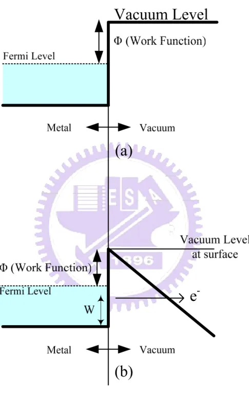
Fig. 1-2(a) showed the band diagram of a metal-vacuum system without an external bias applied. The energy required to make electrons be extracted from the Fermi level of a metal to a rest position of vacuum is named as the work function φ. When a bias is applied, vacuum energy level is lowered and therefore the potential barrier at the surface becomes narrower as shown in Fig. 1-2(b). Afterward, an electron which acquires energy “W” has a finite probability to tunnel through the surface barrier. Fowler and Nordheim deriving the famous F-N equation (1.1) is as followed [1.7]:
( )
exp[ 2 ( )/ ] 3 2 2 E y v B y t AE J φ φ − = , (1-1)where J is the current density (A/cm2), E is the applied electric field (V/cm), φ is the work function (in eV), A = 1.56×10⁻⁶, B = -6.831×10⁻⁷, y = 3.79×10⁻⁴E1/2/φ, t2(y)~1.1 and v(y)
), 5 . 0 cos( ) (y y v = π (1-2) or . 95 . 0 ) (y y2 v = − (1-3)
Typically, the field emission current I is measured as a function of the applied voltage V. Substituting relationships of J = I/α and E = βV into Eq.(1-1), where α is the emitting area and β is the local field enhancement factor of the emitting surface, the following equation can be obtained ] ) ( exp[ ) ( 2 3 2 2 2 V y Bv y t V A I β φ φ αβ − = , (1-4) Then take the log. form of Eq. (1-4)
) ) ( ( 10 97 . 2 ] ) ( 10 54 . 1 log[ ) log( 2 3 7 2 2 6 2 V y v y t V I β φ φ αβ − × × = − , (1-5)
From Eq. (1-5), the slope of a Fowler-Nordheim (F-N) plot is given by
) ( 10 97 . 2 2 3 7 β φ × − = ≡slopeFN S , (1-6)
The parameter β could be evaluated from the slope S of the measured F-N plot if the work function φ was known
) ( 10 97 . 2 2 3 7 S φ β =− × (cm-1), (1-7)
The emission area α can be subsequently extracted from a rearrangement of Eq. (1-5)
) 10 53 . 6 exp( ) 89 . 9 exp( 10 4 . 1 ) ( 2 3 7 2 6 2 V V I β φ φ β φ α − × × = − (cm2), (1-8)
For example, the electric field at the surface of a spherical emitter of radius r concentric with a spherical anode (or gate) of radius r+d can be represented analytically by
) ( d d r r V E= + , (1-9)
Though a realistic electric field in the emitter tip is more complicated than above equation, we could multiply Eq.(1-9) by a geometric factor β` to approximate the real condition.
≡ tip E function of (r,d) =β` ( ) d d r r V + , (1-10)
where r is the tip radius of emitter tip, d is the emitter-anode(gate) distance and β` is a geometric correction factor [1.17].
For a very sharp conical tip emitter, where d >> r, Etip approaches to β`(V/r). And for
r>>d, Etip approaches to β`(V/d) which is the solution for a parallel-plate capacitor and for a
diode operation in a small anode-to-cathode spacing. As the gated field emission array (FEA) with very sharp tip radius, Eq. (1-10) can be approximated as:
Etip =β`(V/r). (1-11)
Combining E= βV and Eq. (1-11), we can obtain the relationship:
Etip =βV =β`(V/r), and β`= βr. (1-12)
The tip radius r is usually in the range from a few nm to 50 nm, corresponding to the parameter β` ranging from 10-1 to 10-2.
Besides, transconductanceg of a field emission device is defined as the change in anode m current due to a change in gate voltage [1.6].
g C m V I g ∂ ∂ = |Vc , (1-13)
of current charge that can be accomplished by a given change in grid voltage. The transconductance could be increased by using multiple tips or decreasing the cathode-to gate spacing for a given cathode-to-anode spacing.
According to the equations mentioned previously (especially Eq.1-5), some approaches could be taken to reduce the operating voltage of the field emission devices, including increasing the aspect ratio of emission cathodes, lowering the work function of emitter materials, fabricating protrusions, increasing emission sites, narrowing the cone angles of field emitters.
1.2 The Application of Vacuum Microelectronics
Vacuum microelectronics devices may contain two parts: one is that devices require large area of cathodes and in the meanwhile use micro-fabricated sources to achieve high current density, fast current control with low voltages. These kinds of devices include electron guns for microwave beam tubes, emission sources for displays etc.. The other is that devices themselves are small and hence require small electron source. Such devices contain micro-triodes, power generators for infrared or optical frequencies etc..
1.2.1 Overview of the Application of Vacuum Microelectronics
Owing to the superior properties of vacuum microelectronic devices, such as fast carrier drift velocity, temperature insensitivity, and radiation hardness, there are plenty of potential applications for vacuum microelectronics. A great number of applications have been proposed, including high efficiency microwave amplifier and generator [1.18-1.20] (Fig.1-3), high brightness flat-panel display [1.21-1.25] (Fig.1-4), scanning electron microscopy, electron beam lithography, micro-sensor [1.26-1.27] (Fig.1-5), ultra-fast computer, intense electron/ion sources [1.28-1.29] (Fig.1-6), temperature insensitive electronics, and radiation hardness analog and digital circuits.
1.2.2 Vacuum Microelectronics Devices for High Frequency Application
Both solid-state devices and vacuum devices could generate power at frequency in the GHz range, but only vacuum devices remain the technology available for high power and high frequency applications. This is because that when the applied voltages are high, there is enough energy for electrons to accelerate to the velocity faster than the saturation velocity in semiconductor and therefore the fast electrons could reduce transit time for high frequency
operation. These devices contain traditional multi-terminal vacuum tubes, such as triodes, pentodes, and beam power tubes, and distributed-interaction devices, including traveling wave tubes (TWTs), klystrons, backward-wave oscillators (BWOs).
The performance of conventionally modulated power tubes using FEAs, such as TWT, is determined basically by emission current and current density capability. On the other hand, the application of FEAs in the microwave tubes in which modulation of the beam is accomplished by capacitance and transconductance. A gated FEA in a 10 GHz TWT amplifier with conventional modulation of electron beam has been proposed by NEC Corporation of Japan [1.30]. The amplifier utilized a modified Spindt-type Mo cathode which incorporated a resistive poly-Si layer as a current limiting element. The emission current from the cathode was 58.6 mA. Besides, the structure owns a low resistance under normal operation, so it could operate at 10.5 GHz with the output power of 27.5 W and the gain of 19.5 dB.
1.3 Lateral Field Emission Array
1.3.1 Comparison between Lateral and Vertical Field Emission Array
There are two basic types of field emission arrays: one is vertical type, and the other is lateral one. In the vertical field emission array, the distance between anode and cathode is difficult to control exactly, and the incorporation of a collector needs extra complicated steps to form a cantilevered electrode [1.31-1.32] (Fig.1-7). Therefore, this kind of vertical structure increases fabrication complexity and cost. Compared with vertical field emitters, lateral-type [1.33] (Fig. 1-8) emitters own a great number of advantages, including ease of fabrication, design versatility of electrode geometry and better gap-controlling ability than vertical type emitters.
1.3.2 Fabrication of Lateral Field Emitters
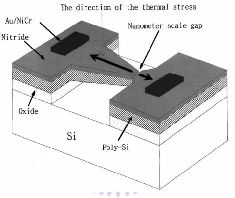
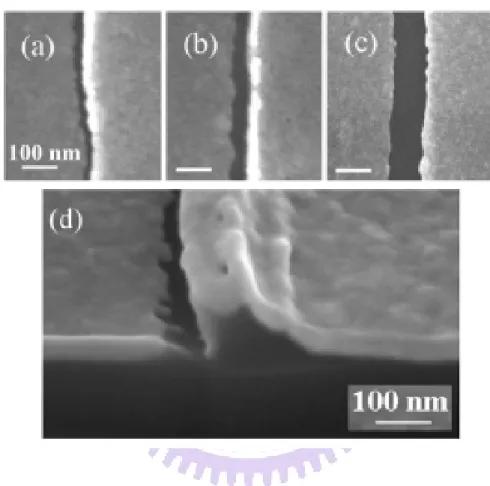
In order to reduce the operation voltage of field emission array to lower power consumption, there are a great many of methods have been proposed to fabricate a small distance between anode and cathode for lateral field emission array. A gap could be produced by high resolution electron beam lithography (EBL) and etching process [1.34] (Fig.1-9). Besides, focused ion beam (FIB) is another method to fabricate wedge type field emitters [1.35] (Fig.1-10). In addition, some small gaps were produced by stress to cleave during annealing (Fig.1-11), oxidation (Fig. 1-12), and phase transformation [1.36-1.38] (Fig.1-13).
1.4 Motivation
In order to improve field emission characteristics of field emission devices to apply on high performance devices, lower operation voltage and higher field emission current are necessary in field emission devices. Consequently, the aim of this essay is concentrated on reducing operation voltage and increasing field emission current density of field emitters. Moreover, lateral types of field emitters are adopted due to the advantages of lateral field emitters in comparison with vertical field emitters mentioned previously. In addition, the fabrication temperatures are also controlled to be as low as possible to reduce cost and utilize glass substrate to replace silicon substrate in the future.
1.4.1 Lower Operation Voltage of Field Emitter by Structure Improvement
For the sake of reducing operation voltage, it is essential to reduce the distance between anode and cathode of field emitters. There are lots of methods have been proposed to produce the small anode-to-cathode gaps, including high resolution electron beam lithography (EBL), focused ion beam (FIB) and producing small cracks by thermal or phase transformation stress. Nevertheless, the throughput of EBL and FIB is low, and the gaps fabricated by thermal and phase transformation are difficult to be controlled exactly. Besides, extra cost will be increased during long-time and high-temperature process, such as annealing and oxidation.
In this essay, thin-film edge emitters are proposed to reduce the operation voltage. In these kinds of structures, the distance between anode and cathode is controlled by the thickness of inter layer and hence could be defined precisely. Furthermore, different metal thin films are deposited to improve field emission characteristics by being treated with hydrogen and ethylene to change the morphologies of surface or physical properties. In addition, the throughput of these structures is higher than that of structures fabricated by EBL or FIB.
1.4.2 Enhance Field Emission Current Density by Carbon Nanotubes
Since carbon nanotubes were discovered by Sumio Iijima in 1991 [1.39] (Fig.1-14), they have attracted a great deal of interest due to their unique properties and potential applications. Carbon nanotube is considered as one of the most promising field emission materials owing to its special properties, such as high aspect ratio, strong mechanical strength, chemical inertness and good thermal conductivity. Consequently, two types of CNT-based lateral field emission devices are proposed in this essay to enhance field emission current density.
1.5 Thesis Organization
In chapter 1, the overview of vacuum microelectronics including history, basic theory background, applications and motivation is described. In chapter 2, thin-film edge field emitters are proposed to reduce the operation voltage. In these kinds of structures, the distance between anode and cathode could be defined precisely by controlling the thickness of inter layer. Besides, different metal thin films are deposited to enhance field emission characteristics. Afterward, the forming processes which followed metal thin-film deposition to improve field emission characteristics are inspected.
Lateral field emitters combined with carbon nanotubes are proposed in chapter 3. Carbon nanotubes are applied on these kinds of field emitters to take advantages of field enhancement factor. For the sake of improving field emission current density, the trench-type lateral field emission device is developed based on the co-planar-type lateral field emission device mentioned previously. In the end, the summary and conclusions are explicated in chapter 4.
Chapter 2
Fabrication and Field Emission Characteristics of
Thin Film Edge Emitters
2.1 Introduction
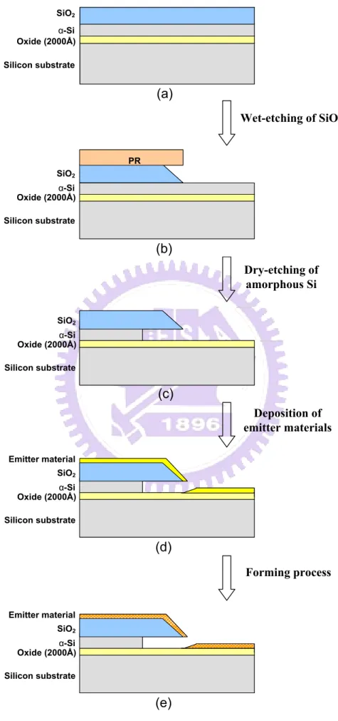
For the sake of improving the field emission characteristics of devices to be applied on high performance devices, it is essential to reduce the operation voltage of field emitters and hence the distance between anode and cathode must be small enough. In this chapter, a kind of thin film edge emitters with a small gap between emitter and collector is proposed. The size of the gaps is controlled by the thickness of inter layer (amorphous silicon) and could be defined precisely. Furthermore, different emitter materials are deposited to take advantages of their own field emission characteristics. In addition, the samples are loaded into thermal CVD chamber to change the morphologies and chemical properties of the emitter materials to improve field emission characteristics. The schematic diagram of the whole experimental procedures is illustrated in Fig. 2-1
2.2 Experimental Procedures
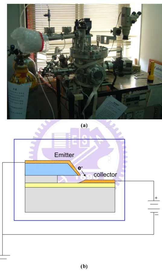
Fig. 2-2 shows the schematic diagram of the fabrication procedures of a thin film edge emitter. In the beginning, wet oxide (200 nm), amorphous silicon and TEOS oxide (500 nm) were sequentially deposited on the (100) p-type wafer by furnace. In this deposition step, the small gaps between collector and emitter were decided by the thickness of amorphous silicon as 150, 300, and 450 nm and could be defined precisely owing to stable deposition parameters. After the first lithography, TEOS oxide was wet-etched to become hard mask and then the photo-resist was removed by acetone. Then, amorphous silicon was dry-etched by dielectric reactive ion etcher (dielectric RIE; SAMCO RIE200L) with TEOS oxide as hard mask to produce undercut of amorphous silicon. After the second photolithography, the metal thin films as field emitter materials were deposited by dual E-gun evaporator (JAPAN ULVAC EBX-10C) and magnetron sputtering (Ion Tech Microvac 450CB). In the end, samples with different field emitter materials were loaded into thermal CVD system to be treated and this step is called forming process. The atmospheric pressure thermal CVD system is composed of a 2-in.-diameter horizontal quartz tube, an electric heating system, reaction gas supply and related mass flow controllers (Fig. 2-3).
The morphologies of the samples with different field emitter materials which were untreated or treated by thermal CVD system were characterized by scanning electron microscopy (SEM; Hitachi S-4700I) and atomic force microscope (AFM; Veeco Dimension 5000 Scanning Probe Microscope (D5000) ). Field emission characteristics of thin film edge field emitters were measured with the pressure of 5×10⁻⁶ Torr. Anode voltages were applied with a source measure unit (Keithley 237) while the cathode was biased at 0 V. The high vacuum measurement system is shown in Fig. 2-4
2.3 Experimental Design
After the structures of thin film field emitters were fabricated, different field emitter materials were deposited on the samples and the patterns of these field emitter materials were defined through photolithograph and lift off process.
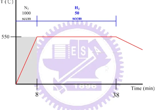
In the first part of experiment of thin film edge field emitters, the Cr thin film (1000 Å) and the bi-layered thin film (W/Ti, 500/100 Å) which were composed of Ti and W sequentially deposited were chosen to be electrodes. Both the samples with Cr thin film and bi-layered thin film were loaded into thermal CVD system to be treated at 550℃ for 30 minutes with 50 sccm C2H4 and 100 sccm H2 (shown in Fig. 2-5) to improve field emission
characteristics. One of the electrode materials was selected to be electrodes according to its better electrical characteristics.
In the second part of experiment of thin film edge field emitters, extra thin films, including Co (50 Å) and Pd (50 Å) were deposited individually on the electrodes to be expected to improve field emission characteristics. After deposition, the samples with different field emitter materials were also treated by forming process to improve field emission characteristics. There were two kinds of forming processes; one of the forming processes was that samples were treated at 550℃ for 30 minutes with 50 sccm H2 (shown in
Fig. 2-6) and the other forming process was that treated at 550℃ for 30 minutes with 20 sccm C2H4 and 500 sccm N2 (shown in Fig. 2-7). These forming processes were expected to change
2.4 Results and Discussion
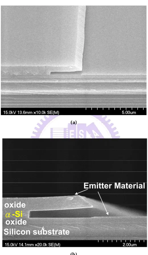
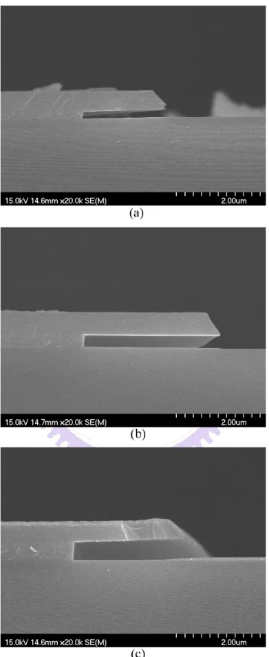
The tilted and cross-sectional SEM images of thin film edge emitters are shown in Fig. 2-8(a) and Fig.2-8(b), respectively. The length of emission edge was fixed at 200 μm. The small gap between emitter and collector was fabricated by dry-etching of amorphous-silicon layer to produce undercut. In order to clarify the field emission characteristics of thin film edge emitters, three kinds of gaps were designed by change of the thickness of amorphous-silicon layer as 150, 300, 450 nm (Fig. 2-9) and could be controlled precisely due to the stable amorphous-silicon deposition parameters.
2.4.1 The Selection of Field Emitter Electrode: Cr and W/Ti
The SEM images of Cr thin film and bi-layered thin film (W/Ti, 500/100 Å) are shown in Fig. 2-10 and Fig. 2-11, respectively. It could be observed that after forming process, the morphologies of Cr and W/Ti became rougher. To know more details, the AFM images of Cr thin film and bi-layered thin film (W/Ti, 500/100 Å) before and after forming process shown in Fig. 2-12 and Fig. 2-13 are also checked. The Rms of Cr and W/Ti are also showed in Table 2-1. The scan area of AFM for the samples was 3×3 μm2. The mean roughness of Cr thin film before forming was 0.987 nm (Rms = 1.286 nm) and was 2.086 nm (Rms = 2.629 nm) after forming. The Rms of W/Ti before forming was 0.94 nm and was 1.258 nm after forming. These results were consistent with SEM images. The increase of surface roughness of Cr thin film and the bi-layered thin film (W/Ti) was conjectured as formation of carbide phase by thermal reaction after forming process [2.1] and therefore could improve the field emission characteristics [2.2-2.3]. In addition, the thickness of W was not so thin and the moving ability of W atoms on the surface was not strong due to the higher melting point and hence the stronger binding energy, and therefore the roughness of W was not obvious as that of Cr after forming process.
The field emission characteristics of Cr thin film and bi-layered thin film (W/Ti, 500/100 Å) with different emitter-to-collector gaps were shown in Fig.2-14 and Fig. 2-15, respectively. The field emission currents (I) were measured as a function of collector voltage (V) sweep from zero to appropriate positive voltages. The length of emission region is designed as 200 μm, and the turn-on voltage is defined as the emission current achieved 10-7 A. The turn-on voltages of Cr and W/Ti thin film field emitters were shown in Table 2-2.
From Fig. 2-14(a), it revealed that field emission characteristics of Cr thin film edge field emitters with emitter-to-collector gap fixed at 150 nm were improved greatly after forming process, including increase of field emission current and reduce of turn-on voltage. The turn-on voltage of Cr thin film edge emitter before forming process was 115 V and reduced to 10 V after forming process, which has the field emission current could as high as 1.44×10⁻⁵ A when the collector was biased at 30 V. Besides, the field emission current was increased and the turn-on voltage was reduced accompanied the narrowing of emitter-to-collector gap. The turn-on voltage of Cr thin film emitters were 15 and 17.5 V with gap fixed at 300 and 450 nm, and it reduced to 10 V when the gap was fixed at 150 nm. Because of the lowering of gaps, electrons were more easily to be extracted from metals.
From Fig. 2-15(a), it could be observed that field emission characteristics of W/Ti thin film edge field emitters with emitter-to-collector gap fixed at 150 nm were also improved after forming process. The turn-on voltage of W/Ti thin film edge emitter before forming process was 62 V and reduced to 15 V after forming process, which has the field emission current as high as 9.73×10⁻⁶ A when the collector was biased at 30 V. Furthermore, due to the narrowing of emitter-to-collector gaps, the field emission characteristics of W/Ti thin film emitters were improved. The turn-on voltage of W/Ti emitters were 40 and 62 V with gap fixed at 300 and 450 nm, and it reduced to 15 V when the gap was fixed at 150 nm.
The corresponding F-N plots of the Cr and W/Ti thin film edge emitters are shown in Fig.2-14(b) and Fig.2-15(b), respectively. As could be seen, nearly straight lines with negative
slope at large voltage region were observed, indicating the field emission phenomena of thin film edge emitters.
The improvement of field emission characteristics of thin film edge emitters may because the increase of roughness on the surface of metal thin films enhanced field emission due to formation of carbide phase after forming process. The improvement of field emission characteristics of W/Ti emitters was not obvious as that of Cr emitters due to less increase of roughness of W/Ti surface.
In addition, the improvement of field emission characteristics for both Cr and W was conjectured as increase of roughness rather than reduction of work function. This was because that the work function of carbide phase was almost the same or slightly lower than that of pure metal thin film [2.4-2.5]. Furthermore, the change of work function of binary compound was affected by both work functions of the elements [2.6]. Since the work function of carbon is thought as 4.7~5 eV and almost the same as that of the metal thin film used in the experiments, the improvement of field emission characteristics was regarded as the increase of roughness of surface.
Although the field emission characteristics of Cr thin film edge emitters were better than those of W/Ti thin film edge emitters, the electrode material was selected as W/Ti because of the failures of Cr thin film emitters due to joule heating or local arcing produced by large field emission current density passing through small emission area during measurement [2.7-2.9] (Fig.2-16). The failure phenomena of W is not obvious attributed to the higher melting point of W compared with Cr and therefore W showed higher enduring ability of joule heating.
2.4.2 The Discussion of Field Emitter Material (1): Co
Cobalt thin film (Co, 50 Å) was deposited on the W/Ti (500/100 Å) to expected to improve field emission characteristics by increase of roughness of the surface. However, when Co thin film treated with C2H4 and H2 (the forming process for Cr and W/Ti) in the
same time, carbon nanotubes would tend to be produced and resulted in short circuit between anode and cathode easily (Fig.2-17). Consequently, the forming processes were designed as treated with H2 and treated with C2H4 individually to improve field emission characteristics of
Co thin film field emitters.
There were two kinds of forming processes mentioned in 2.3 for Co thin film edge field emitters to be treated. The SEM images of Co thin film before and after forming processes are shown in Fig. 2-18 and from them could be observed that morphologies of Co thin film became rougher after the two forming processes. Besides, the morphologies were also examined by AFM images of Co thin film before and after forming processes shown in (Fig. 2-19). The mean roughness of Co thin film before forming was 1.021 nm (Rms = 1.291 nm) and became 4.291 nm (Rms = 6.439 nm) and 7.111 nm (Rms = 9.134 nm) after treated with H2 and C2H4, respectively. After treated with H2 at 550℃, Co thin film was transformed into
nano-particles due to thermal energy therefore increasing the roughness of metal surface and H2 was used to reduce the metal. After treated with C2H4, Co thin film was assumed to
increase roughness by carbide formation [2.10-2.12] and graphite layers production [2.12-2.13]. At the beginning of C2H4 treatment, C2H4 was decomposed on the surface of Co
and diffused into Co particles, and carbide phase and graphite layers was produced during cooling [2.12-2.13]; therefore, these phenomena increased the roughness of Co surface at the same time. The field emission characteristics of Co thin film edge emitters before and after treated with H2 and C2H4 are shown in Fig. 2-20 and Fig. 2-21, respectively. The turn-on
Table 2-3. The turn-on voltage of Co thin film edge emitter with emitter-to-collector gap fixed at 150 nm before forming process was 112 V and reduced to 12 V after treated with H2, which
has the field emission current as high as 1.63×10⁻⁶ A when the collector was biased at 40 V. Furthermore, the increase of field emission current and reduce of the turn-on voltage accompanied the narrowing of emitter-to-collector gap due to ease of extraction of electrons. The turn-on voltage of Co thin film emitters were 28 and 50 V with gap fixed at 300 and 450 nm, and it reduced to 12 V when the gap was fixed at 150 nm.
The turn-on voltage of Co emitter with gap fixed at 150 nm reduced to 8 V after treated with C2H4 and the field emission current could achieve 1.9×10⁻⁵ A when the collector was
biased at 40 V. Besides, the turn-on voltage of Co thin film emitters were 20 and 43 V with gap fixed at 300 and 450 nm, and reduced to 8 V when the gap was fixed at 150 nm.
The corresponding F-N plots of the Co thin film edge emitters are shown in Fig.2-20(b) and Fig. 2-21(b). It revealed that straight lines with negative slope at large voltage region, and also indicated the field emission phenomena of thin film edge emitters.
Field emission characteristics were improved by forming processes to increase roughness of the surface of Co thin film. In addition, Co thin film edge emitters treated with C2H4
showed better field emission characteristics than those treated with H2 owing to rougher
surface. The roughness was attributed to the carbide and graphite layer formation to enlarge the field enhancement factor.
In addition, the main reason for improvement of field emission characteristics of Co was conjectured as increase of roughness instead of reduction of work function due to carbide formation. The reason was the same as the reason mentioned in 2.4.1. There was no obvious difference of work function between Co and C, and therefore the reduction of work function due to carbide formation wasn’t apparent.
2.4.3 The Discussion of Field Emitter Material (2): Pd
Palladium thin film (Pd, 50 Å) was another field emitter material deposited on the W/Ti (500/100 Å) to improve field emission characteristics and the two kinds of forming processes mentioned previously were also adopted.
The SEM images of Pd thin film before and after the two forming processes are shown in Fig. 2-22. It revealed that the increase of roughness after the two forming processes was not very obvious. After treatments, the phase transformation of Pd would take place, the carbon atoms would diffuse into the interstitial positions and hydrogen atoms would diffuse into both the interstitial and substantial positions of Pd and resulted in lattice expansion of Pd [2.14-2.15]. However, the roughness of Pd thin film after treatment was not apparent. This was conjectured that the under layer of Pd, W, has the higher surface energy than Pd and hence the roughness of Pd was not so obvious. The morphologies were also checked by AFM images shown in Fig. 2-23. The mean roughness of Pd was 0.802 nm (Rms = 1.028 nm) before forming process, and was 1.106 (Rms = 1.394 nm) and 0.909 nm (Rms = 1.152 nm) after forming treated with H2 and C2H4, respectively. These results were also consistent with
SEM images.
The field emission characteristics of Pd thin film edge emitters before and after treated with H2 and treated with C2H4 are shown in Fig. 2-24, and Fig.2-25, respectively. The turn-on
voltages of Pd thin film field emitters treated with both forming processes were shown in Table 2-4. The turn-on voltage of Pd thin film edge emitter with emitter-to-collector gap fixed at 150 nm before forming process was 114 V and reduced to 25.5 V after treated with C2H4,
which has the field emission current as high as 3.59×10⁻⁷ A when the collector was biased at 40 V. Besides, the turn-on voltage of Co thin film emitters were 71 and 84 V with gap fixed at 300 and 450 nm, and it reduced to25.5 V when the gap was fixed at 150 nm.
with H2 could be observed in Fig. 2-24(a). The turn-on voltage of Pd emitter with
emitter-to-collector gap fixed at 150 nm before forming process was 114 V and reduced to 6.5 V after treated with H2, which has the field emission current as high as 5.67×10⁻⁵ A when the
collector was biased at 40 V. Besides, the turn-on voltage of Pd thin film emitters were 10.5 and 16 V with gap fixed at 300 and 450 nm, and it reduced to 6.5 V when the gap was fixed at 150 nm.
The corresponding F-N plots of the Pd thin film edge emitters are shown in Fig.2-24(b) and Fig. 2-25(b). The straight lines with negative slope at large voltage region could be seen, and it indicated the field emission phenomena of thin film edge emitters.
Although there was no apparent difference between the morphologies of Pd surface after the two forming processes, the improvement of field emission characteristics of the samples treated with H2 were greater than those treated with C2H4, including increase of field emission
current and reduce of turn-on voltage. This was conjectured that PdHX would be produced
after Pd thin film treated with H2, and the work function of PdHX was lower than pure Pd
[2.16-2.18]. Besides, although the treatment of C2H4 would provide hydrogen atoms for Pd
thin film, the PdHX production would be suppressed by the competition between PdCX and
PdHX [2.14-2.15]. Additionally, the flow rate of H2 (50 sccm) was larger than the flow rate of
C2H4 (20 sccm) and hence the formation of PdHX for Pd treated with C2H4 was not obvious.
Consequently, the field emission characteristics of Pd thin film edge emitters treated with H2
were improved greatly than those treated with C2H4.
2.4.4 The Comparison for Different Field Emitter Materials
Due to the thickness of electrode materials was much thicker than Co and Pd thin films, the comparison was divided into two parts: one was about electrode material, and the other was about emitter thin film.
The original work function and the morphologies of Cr and W/Ti electrode materials are shown in Table Table 2-5. The increase of roughness was due to formation of carbide phase after treatment and therefore improved the field emission characteristics. The roughness of Cr after forming process was larger than that of W. This was inferred that melting point of W was much larger than Cr and thus the weaker moving ability of atoms due to stronger bonding energy resulted in less increase of roughness. Therefore, the improvement of field emission characteristics of Cr was greater than that of W due to larger roughness.
The original work function of Co and Pd thin films and the morphologies of Co and Pd thin films before and after the two forming processes are shown in Table 2-6. And the field emission characteristics of the Co and Pd emitters are shown in Fig. 2-26.
Due to the surface energy ranking: W > Co > Pd [2.19], the roughness of Co after treated was larger than Pd. This was because that the surface energy of the under-layer, W, is larger than both Co and Pd; therefore, the surface of W didn’t attempt to be bared. Besides, the difference of surface energy between Pd and W is more obvious than that between Co and W and hence the effect is more apparent in Pd thin film edge emitters.
With almost the same morphologies before and after forming processes, Pd thin film edge emitters treated with H2 showed better field emission characteristics than samples treated
with C2H4 and that was conjectured to be PdHX production accompanied forming process to
reduce work function [2.16-2.18].
Compared H2 treatment with C2H4 treatment of Co thin films, the morphologies of Co
thin film edge emitters treated with C2H4 were rougher than those treated with H2 and hence
the field emission characteristics of Co emitters treated with C2H4 were greater than treated
with H2. Besides, the main reason for great improvement of Co thin film edge emitter treated
with C2H4 was attributed to the increase of roughness rather than reduction of work function
resulted from carbide phase.
with C2H4, the work function reduction of Pd thin film by production of PdHX resulted in
greater improvement of field emission characteristics than the roughness increase of Co thin film by carbide and graphite layers productions. These results revealed that the contribution of work function reduction on improving field emission characteristics was more efficient than the contribution of roughness.
The turn-on voltage of the thin film edge emitters with emitter-to-collector fixed as 150 nm are shown in Table 2-7 and Fig. 2-27. The Co thin film edge emitters treated with C2H4
and the Pd thin film edge emitters treated with H2 showed lower turn-on voltages among the
samples were selected to do electrical stress test (Fig. 2-28). The stress parameters were that field emission current was fixed at 1 μA with appropriate collector bias and stress time was one hour. Due to the failures of Cr thin film emitters attributed to large current passing through small devices and therefore resulting in joule heating or local arcing, Pd emitters with higher melting point (1552℃) than Co (1495℃) were expected to demonstrate more stable electrical characteristic during stress test. The assumption was consistent with experimental results that the fluctuation of Co thin film emitters was from -56.3% to +26.7% and of Pd thin film was from -15.7% to +10.3%. Besides, the fluctuation of both emitters became stable after 1500 seconds.
2.5 Summary
In order to reduce the operation voltage of field emitters, the distance between emitter and collector must be narrowed. In this chapter, thin film edge emitters with small emitter-to-collector gap were proposed to reduce operation voltage. The distance of gap was decided by the thickness of amorphous silicon at the first deposition step and therefore could be controlled precisely.
At first, either Cr thin film or bi-layered thin film (W/Ti, 500/100 Å) would be selected as electrodes. The bi-layered thin film (W/Ti, 500/100 Å) was decided to be electrode because of the failures of Cr thin film emitters due to joule heating or local arcing produced during measurement.
For the sake of improving field emission characteristics, Cobalt thin film (Co, 50 Å) and Palladium thin film (Pd, 50 Å) were deposited. The field emission characteristics of Co thin film emitters treated with C2H4 were enhanced due to increase of roughness of Co surface.
The turn-on voltage of Co emitter with gap fixed at 150 nm reduced to 8 V after treated with C2H4 and field emission current of 1.9×10⁻⁵ A could be achieved when the collector was
biased at 40 V. The field emission characteristics of Pd thin film were improved by PdHX
production during treatment with H2 because of the lower work function of PdHX than pure
Pd. The turn-on voltage of Pd emitter with emitter-to-collector gap fixed at 150 nm was down to 6.5 V after treated with H2 and field emission current of 5.67×10⁻⁵ A could be achieved
Chapter 3
Fabrication and Field Emission Characteristics of
CNT-based Lateral Field Emitters
3.1 Introduction
Carbon nanotube is considered as one of the most promising field emission materials due to its special properties, such as high aspect ratio, strong mechanical strength, chemical inertness and good thermal conductivity [3.1-3.4]. In this chapter, lateral field emission devices with incorporation of carbon nanotubes as field emission materials are proposed to enhance field emission current density. In addition, two kinds of lateral field emitters are fabricated; one is a co-planar lateral field emission device, and the other is a step-type field emission device. The step-type lateral field emission devices are expected to show lower operation voltage than basic lateral ones to reduce power consumption.
3.2 Experimental Procedures
3.2.1 Co-Planar-Type Lateral Field Emission Devices
Fig. 3-1 shows the schematic diagram of the fabrication procedures of lateral field emission devices. First, a film of oxide (1 μm) was deposited on the (100) n-type silicon wafer by PECVD. After first photolithography and wet-etching of oxide, the position of contact hole was defined. Then, chromium thin film (Cr, 1000 Å) was deposited as electrodes by dual E-gun evaporator (JAPAN ULVAC EBX-10C). After the second photolithography, the Cr thin film was wet-etched to decide the shape of electrode. Afterward, the third photolithography was proceeded and Cr thin film was wet-etched to produce undercut to define the distance between anode and cathode as 2, 3, 4 μm. A multi-layered catalyst composed of Al (100 Å), Ti (30 Å), and Co (10 Å) was sequentially formed on Cr electrode by magnetron sputtering (Ion Tech Microvac 450CB) and lift-off process. Then the samples were loaded into thermal CVD system for CNT growth. Prior to the CNT growth, hydrogen with 50 sccm was fed into the chamber for 5 minutes for pretreatment of catalyst. During CNT-growth period, reaction gases consisting of nitrogen (N2, 1000sccm), hydrogen (H2, 10
sccm) and ethylene (C2H4, 125 sccm) were fed into chamber at 550℃ for 30 minutes to grow
CNTs (Fig.3-2 ).
The morphologies of the samples were examined by scanning electron microscopy (SEM; Hitachi S-4700I). The fine structures of carbon nanotubes and elements of nano-particles of catalyst were characterized by high-resolution transmission electron microscopy (HRTEM; JEOL JEM-2000EX) and X-ray energy dispersive spectroscopy (EDS), respectively. The crystallization and defect conditions of carbon nanotubes were examined by Raman spectrum (Jobin Yvon LABRAM HR Micro-Raman system). Field emission characteristics of lateral field emission devices combines with carbon nanotubes were measured in a high-vacuum chamber with the pressure of 5×10⁻⁶ Torr. Anode voltages were applied with a source
measure unit (Keithley 237) for the verification of field emission characteristics while the cathode was biased at 0 V. The diagram of field emission measurement for lateral field emitters is shown in Fig. 3-3.
3.2.2 Step-Type Lateral Field Emission Devices
Fig. 3-4 shows the schematic diagram of the fabrication procedures of step-type lateral field emission devices. First, oxide and chromium thin film (Cr, 1000 Å) were deposited on the (100) n-type silicon wafer. In this step, the depth of step-type lateral field emission devices was decided by the thickness of the oxide as 0.5 and 1 μm, respectively. After the first photolithography, Cr thin film was wet-etched to pattern the shape of electrode. After the second photolithography, Cr thin film and oxide were wet-etched, respectively. Then, the gap between collector and emitter was decided by wet-etching of Cr thin film to formed undercut as 2μm. Afterward, a multi-layered catalyst composed of Al (100 Å), Ti (30 Å), and Co (10 Å) was sequentially deposited on Cr electrode by magnetron sputtering (Ion Tech Microvac 450CB) and lift-off process. The samples were loaded into thermal CVD system to grow carbon nanotubes, and the growth parameters are the same as mentioned previously.
The morphologies, fine structures, crystallization and defect conditions of carbon nanotubes were characterized by the same instruments mentioned above. The field emission characteristics of step-type field emission devices were measured with a source measure unit (Keithley 237) in a high-vacuum chamber with the pressure of 5×10⁻⁶ Torr. The diagram of field emission measurement for step-type lateral field emitters is shown in Fig. 3-5.
3.3 Results and Discussion
3.3.1 The Properties of Carbon Nanotubes
The SEM images of carbon nanotubes grown at 550℃ using multi-layered catalyst composed of Co/Ti/Al (10/30/100 Å) are shown in Fig.3-6. The carbon nanotubes were selectively grown on the catalyst and the average length of carbon nanotubes was 1.3 μm. From TEM images (Fig. 3-7) of carbon nanotubes, it could be found that the closed tip was filled with catalytic nano-particles and the structure of carbon nanotube is multi-walled. There was an amorphous layer covering the nanotube. This result was consistent with Raman spectrum illustrated in Fig.3-8. The carbon nanotubes were grown at low temperature (550℃) and therefore there were a lot of defects existing in the carbon nanotubes. So the intensity of defect (I(D)) represented amorphous carbon shown as D peak was high and the intensity of graphite (I(G)) represented crystallinity of carbon nanotubes shown as G peak was low. The element of catalytic nano-particles was examined by EDS and the results are shown in Fig.3-9. It revealed that the catalyst is composed of cobalt that was also consistent with the experiment.
3.3.2 The Effect of Gap Distance between Emitter and Collector
The cross-sectional and top view SEM images of the lateral field emission devices combined with carbon nanotubes are shown in Fig. 3-10(a) and (b), respectively. Carbon nanotubes were grown on the multi-layered catalyst to be emitter materials and the gap between emitter and collector of lateral field emission devices was controlled by wet-etching of the Cr thin film. For the sake of clarifying the field emission characteristics of lateral field emission devices, three kinds of gaps were fabricated as 2, 3, 4 μm shown in Fig. 3-11.
devices with different emitter-to-collector gaps. The field emission currents (I) were measured as a function of collector voltage (V) sweep from zero to appropriate positive voltages. The length of emission region is designed as 100 μm, and the turn-on voltage is defined as the emission current achieved 10-7 A. The turn-on voltages of co-planar-type field emission devices with different emitter-to-collector gaps were shown in Table 3-1. In Fig. 3-12(a), it could be observed that when the gaps between emitter and collector were reduced, the current would be increased and the turn-on voltage would be lowered. When the gap of the lateral field emission device was 3, 4 μm, the turn-on voltage was 13.5, 22 V, respectively. When the gap of field emission devices was reduced to 2 μm, the turn-on voltage was lowered as 9 V and the field emission current of 1×10⁻⁴ A could be achieved when the collector was biased at
32.5 V. This was because that electrons were more easily to be extracted due to reduce of emitter-to-collector gap. The corresponding F-N plots of the lateral field emission devices combined with carbon nanotubes are shown in Fig.3-12(b). As could be seen, nearly straight lines with negative slope at large voltage region were observed, indicating the field emission phenomena of the lateral field emission devices.
3.3.3 The Effect of Thickness of Oxide under Collector
In order to improve field emission characteristics of lateral field emission devices, another type of field emission devices named step-type field emission devices based on the lateral field emission devices mentioned above was proposed. The cross-sectional SEM image of the step-type field emission device is shown in Fig. 3-13. The effect of thickness of oxide under collector was investigated with the emitter-to-collector gap fixed at 2 μm. The change of the thickness of oxide corresponds to the change of the distance between collector and emitter. On account of clarifying the thickness-effect, three kinds of thicknesses of oxide for the step-type devices were deposited as 0, 0.5, 1μm shown in Fig. 3-14. The top view SEM
![Fig. 1-8 The SEM images of lateral field emitters: finger shape diodes. [1.33]](https://thumb-ap.123doks.com/thumbv2/9libinfo/8254598.171832/67.892.166.778.314.779/fig-images-lateral-field-emitters-finger-shape-diodes.webp)
![Fig. 1-9 The schematic of small gap produced by e-beam lithography. [1.34]](https://thumb-ap.123doks.com/thumbv2/9libinfo/8254598.171832/68.892.199.727.364.772/fig-schematic-small-gap-produced-e-beam-lithography.webp)