國 立 交 通 大 學
電子工程學系 電子研究所碩士班
碩 士 論 文
射頻互補金氧半 E 類功率放大器設計
RF CMOS Class-E Power Amplifier Design
研 究 生:吳家岱 Jia-Dai Wu
指導教授:溫瓌岸 博士 Dr. Kuei-Ann Wen
共同指導:溫文燊 博士 Dr. Wen-Shen Wuen
射頻互補金氧半 E 類功率放大器設計
RF CMOS Class-E Power Amplifier Design
研 究 生:吳家岱
Student :Jia-Dai Wu
指導教授:溫瓌岸 博士
Advisor
:Dr. Kuei-Ann Wen
共同指導:溫文燊 博士 Co-Advisor
:Dr. Wen-Shen Wuen
國 立 交 通 大 學
電子工程學系 電子研究所碩士班
碩 士 論 文
A Thesis
Submitted to Department of Electronics Engineering & Institute of Electronics
College of Electrical & Computer Engineering
National Chiao Tung University
in Partial Fulfillment of the Requirements
for the Degree of Master
In
Electronic Engineering
射頻互補金氧半 E 類功率放大器設計
學生:吳家岱 指導教授:溫瓌岸 博士
共同指導:溫文燊 博士
國立交通大學電子工程學系 電子研究所碩士班
摘 要
本文提出一個完全整合在單一晶片上使用 0.13-μm CMOS 製程的 E 類功率放 大器,此 E 類功率放大器結合了 F 類的前級放大器並採用有限的小面積電感來取 代大面積的射頻阻隔器以易於整合在單一晶片上。此 E 類放大器在輸入功率為 -3dBm、操作頻率為 2.5GHz 之下,可達到 21dBm 的輸出功率和 48.4%的功率增加 效率,在設計的頻帶內,2.3GHz~2.7GHz,功率增加效率仍然可以維持在 44%以 上。且為了增加系統模擬的時間,本文提出此 E 類功率放大器的形為模型。藉由 此形為模型,系統模擬的時間可以減少 93%左右。RF CMOS Class-E Power Amplifier Design
Student:Jia-Dai Wu Advisor:Dr. Kuei-Ann Wen
Co-Advisor:Dr. Wen-Shen Wuen
Department of Electronics Engineering
Institute of Electronics
National Chiao-Tung University
ABSTRACT
An on-chip CMOS Class-E Power Amplifier (PA) implemented in 0.13-µm CMOS
technology is presented. The Class-E PA includes a Class-F driver and replaces a large RF choke with a small finite dc-feed inductor for on-chip integration. The proposed Class-E PA achieves power added efficiency (PAE) of 48.4 % while delivering 21 dBm output power with the input driving power of -3 dBm at 2.5 GHz. In the design band, 2.3 GHz ~ 2.7 GHz, PAE is still above 44%. In order to improve the simulation time of RF/Baseband co-simulation the behavior model of proposed PA is presented. The simulation time of RF/Baseband co-simulation can be reduced about 93% by the proposed behavior model.
誌 謝
很高興能夠順利地完成碩士論文。首先,非常感謝溫瓌岸教授讓我有機會進 入 TWT 實驗室,並給予我們豐富的資源和良好的學習環境。感謝溫文燊教授在研 究上給予方向與耐心的指導,在二位教授用心的指導下,終於完成了這篇碩士論 文。並感謝各位口試委員們-詹益仁教授與陳巍仁教授教授,提供寶貴的建議與 指教。 感謝實驗室的學長姐們的指導與照顧:美芬學姐、嘉笙學長、哲生學長、文 安學長、晧名學長、立協學長、俊閔學長、志德學長、振威學長、俊憲學長、懷 仁學長及彥宏學長等在研究上的意見與幫助。 感謝實驗室的同學們-書旗、建龍、昱瑞、漢健、閎仁、建毓、世基、翔琮、 義凱、凱信、函霖,二年來在課業和日常生活上總是相互的扶持與幫助。還有總 是無願無悔幫忙我們的學弟們-磊中、佳欣、國爵、柏麟、俊彥、謙若、士賢,; 同時也要感謝實驗室的助理們: 苑佳、淑怡、慶宏、恩齊、智伶、嘉誠、苑君、 怡倩,幫忙實驗室裡大大小小的事,讓我們能更專心於研究。 最後,我要感謝家人無怨無悔的付出與支持,並感謝關心我與幫助我的人, 僅以此論文與我的家人及好友分享我的收穫與喜悅,願他們永遠平安、順心。 吳家岱 2007Contents
摘 要 ... I
ABSTRACT... II 誌 謝 ...III
CONTENTS ...IV LIST OF FIGURES... VII LIST OF TABLES...XI TABLE 2.5 COMPARISONS WITH OTHER PUBLISHED PAPERS. 28 ...XI
INTRODUCTION... 1
1.1MOTIVATION... 2
1.2BASIC CONCEPTS OF CLASS-EPA ... 3
1.2.1 Ideal Class-E Power Amplifier... 4
1.2.2 Practical Considerations ... 7
1.2.3 Finite DC-Feed Inductor ... 8
1.2.4 Cascode Topology ... 9
1.3CLASS-FPOWER AMPLIFIER... 11
1.5ORGANIZATION... 16
CHAPTER 2... 17
ON-CHIP RF CMOS CLASS-E POWER AMPLIFIER DESIGN ... 17
2.1THE PROPOSED CLASS-EPOWER AMPLIFIER... 17
2.1.1 Cascode Topology ... 18
2.1.2 Finite DC-Feed Inductor ... 19
2.1.3 Class-F Driver ... 22
2.1.4 Summary... 24
2.2SIMULATION RESULTS... 25
CHAPTER 3... 29
IMPLEMENTATION AND MEASUREMENT RESULTS ... 29
3.1CHIP LAYOUT DESCRIPTIONS... 29
3.2MEASUREMENT RESULTS... 32
3.2.1 Measurement Setup ... 32
3.2.2 Simulation and Measurement Results... 34
CHAPTER 4... 39
4.1BEHAVIOR MODEL OF CLASS-EPA... 39
4.1.1 Input and Output Matching ... 39
4.1.2 Switched-Mode Transistor ... 44
4.2RF/BASEBAND CO-SIMULATION... 46
4.3COMPARISONS OF SIMULATION TIME... 49
CHAPTER 5... 51
CONCLUSIONS AND FUTURE WORKS ... 51
5.1CONCLUSIONS... 51
5.2FUTURE WORKS... 51
APPENDIX 1 ... 53
ANALYSIS OF IDEAL CLASS-E PA WITH FINITE DC-FEED INDUCTOR... 53
APPENDIX 2 ... 58
BEHAVIOR MODEL OF SWITCHED-MODE TRANSISTOR... 58
BIBLIOGRAPHY ... 61
List of Figures
FIGURE 1.1 WIMAX FREQUENCY BAND DESCRIPTIONS FROM 2GHZ TO 6GHZ. ... 1
FIGURE 1.2 CLASS-E POWER AMPLIFIER... 3
FIGURE 1.3 DRAIN VOLTAGE AND CURRENT WAVEFORMS FOR CLASS-E POWER AMPLIFIER. ... 4
FIGURE 1.4 (A)BASIC CIRCUIT OF THE CLASS-EPA.(B)EQUIVALENT CIRCUIT OF THE CLASS-EPA. ... 5
FIGURE 1.5(A)COMMON-SOURCE.(B)COMMON-GATE SWITCH.(C)COMMON-GATE SWITCH COMBINED WITH COMMON-SOURCE STAGE INTO A CASCODE IN ORDER NOT TO PROVIDE LOW-IMPEDANCE LOAD TO THE DRIVING.(D)MAXIMUM VOLTAGE STRESS IS SHOWN FOR EACH CASE ASSUMING THE INPUT SIGNAL VIN SWINGS FROM 0V TO VGG[9]. ... 10
FIGURE 1.6 CLASS-F POWER AMPLIFIER. ... 12
FIGURE 1.7 DRAIN VOLTAGE AND CURRENT WAVEFORMS FOR CLASS-F POWER AMPLIFIER. ... 12
FIGURE 1.8 EER ARCHITECTURE. ... 13
FIGURE 1.9 POLAR TRANSMITTER ARCHITECTURE. ... 15
FIGURE 2.1 THE PROPOSED CLASS-EPA. ... 17
FIGURE 2.2 CASCODE TOPOLOGY.. ... 18
FIGURE 2.3 SCHEMATIC OF CLASS-EPA WITH FINITE DC-FEED INDUCTOR... 19
FIGURE 2.4 CASCODE TOPOLOGY WITH TUNED OUT INDUCTOR LR... 22
FIGURE 2.6 CASCODE CLASS-EPA WITH CLASS-F DRIVER. ... 24
FIGURE 2.7 COMBINE THREE INDUCTORS INTO ONE FOR LAYOUT CONSIDERATIONS... 24
FIGURE 2.8 DRAIN VOLTAGE AND CURRENT OF M1 AND M2. ... 25
FIGURE 2.9 SIMULATION RESULTS OF OUTPUT POWER AND PAE V.S. INPUT POWER... 26
FIGURE 2.10 SIMULATION RESULTS OF OUTPUT POWER AND PAE V.S. FREQUENCY... 26
FIGURE 2.11 SIMULATION RESULTS OF OUTPUT POWER AND PAE V.S. SUPPLY VOLTAGE... 27
FIGURE 2.12 SIMULATION RESULTS OF LSSP ... 27
FIGURE 3.1 SCHEMATIC AND LAYOUT VIEWS OF CLASS-EPA WITHOUT CLASS-F DRIVER. ... 30
FIGURE 3.2 SCHEMATIC AND LAYOUT VIEWS OF CLASS-EPA WITH CLASS-F DRIVER. ... 31
FIGURE 3.3 MEASUREMENT SETUPS OF P1 AND P2. ... 33
FIGURE 3.4 M2 GATE LEAKAGE CURRENT OF (A) SIMULATION RESULT (B) FROM UMC DOCUMENT [19]. ... 35
FIGURE 3.5 SIMULATION RESULTS OF (A) OUTPUT POWER V.S. INPUT POWER (B) POWER GAIN V.S. INPUT POWER (C)PAE V.S. INPUT POWER. ... 36
FIGURE 3.6 SIMULATION RESULTS OF (A) OUTPUT POWER V.S. OPERATING FREQUENCY... 37
FIGURE 3.7 SIMULATION RESULTS OF (A) OUTPUT POWER V.S. SUPPLY VOLTAGE... 38
FIGURE 4.1 CAPACITOR OF (A)UMC MODEL (B) IT EQUIVALENT CIRCUIT... 40
FIGURE 4.2 CAPACITOR’S SP SIMULATION RESULTS OF BEHAVIOR MODEL AND TRANSISTOR LEVEL.... 40
FIGURE 4.4 INDUCTOR’S SP SIMULATION RESULTS OF BEHAVIOR MODEL AND TRANSISTOR LEVEL. .... 41
FIGURE 4.5 INPUT MATCHING OF (A) SCHEMATIC (B) IT EQUIVALENT CIRCUIT... 42
FIGURE 4.6 SP SIMULATION RESULTS OF THE INPUT MATCHING OF BEHAVIOR MODEL AND TRANSISTOR LEVEL... 42
FIGURE 4.7 OUTPUT MATCHING OF (A) SCHEMATIC (B) IT EQUIVALENT CIRCUIT... 43
FIGURE 4.8 SP SIMULATION RESULTS OF THE OUTPUT MATCHING OF BEHAVIOR MODEL AND TRANSISTOR LEVEL. ... 43
FIGURE 4.9 USING ADS SWITCH MODE TO BE THE SWITCHED-MODE TRANSISTOR MODEL. ... 44
FIGURE 4.10 SUMMARY OF STEP 1~STEP 4... 45
FIGURE 4.11 COMPARISONS OF CIRCUIT SIMULATION BETWEEN TRANSISTOR LEVEL AND... 46
FIGURE 4.12 THE THREE-PORT CIRCUIT... 47
FIGURE 4.13 SCHEMATIC OF SIMPLE POLAR TRANSMITTER IN ADS... 48
FIGURE 4.14 SCHEMATIC OF BEHAVIOR MODEL WITHOUT TRANSISTOR M2... 48
FIGURE 4.15 COMPARISONS OF RF/BASEBAND CO-SIMULATION. ... 49
FIGURE 4.16 COMPARISONS OF CIRCUIT SIMULATION TIME. ... 50
FIGURE 4.17 COMPARISONS OF SIMULATION TIME OF RF/BASEBAND SIMULATION... 50
FIGURE A.1 EFFECT OF THE FINITE DC-FEED INDUCTOR ON THE CLASS-EPA ELEMENTS [8]. ... 55
FIGURE A.2 SIMULATION RESULTS AND VERILOG-A CODE OF STEP 1. ... 58
FIGURE A.4 SIMULATION RESULTS AND VERILOG-A CODE OF STEP 3. ... 59 FIGURE A.5 SIMULATION RESULTS AND VERILOG-A CODE OF STEP 4. ... 60
List of Tables
TABLE 2.1 ANALYSIS OF SUPPLY VOLTAGE. ... 18
TABLE 2.2 DESIGN PARAMETERS. ... 20
TABLE 2.3 DESIGN PARAMETERS. ... 20
TABLE 2.4 DESIGN PARAMETERS. ... 21
Table 2.5 Comparisons with other published papers. 28 TABLE A.1 CLASS-EPA ELEMENTS AS FUNCTION OF THE dc dc R X RATIO [8]. ... 55
Chapter 1
Introduction
Recently, the IEEE has come up with a new standard, 802.16e, is so-called WiMAX (World Interoperability for Microwave Access). WiMAX provides high data rates and long connection distances for residential and enterprise use. The modulation used to achieve high data rates is Orthogonal Frequency Division Multiplexing (OFDM). The modulated signals will display a high Peak-to-Average Power Ratio (PAPR) and a strict linearity requirement in transmitter. Beside, WiMAX also supports roaming which provides each user a connection with cell phone quality, therefore, a wide output power range is necessary. Figure 1.1 shows the WiMAX frequency band descriptions from 2 GHz to 6 GHz.
1.1 Motivation
As the growth of wireless communication networks, there is constantly increasing demand for compact, low-cost and low-power portable devices. This motivates the investigation of single-chip transceivers realized in low-cost CMOS technology. A major difficulty to achieve the fully-integrated transceiver design is the complete integration of PA. The inability to provide on-chip solutions for RF PAs arises primarily from two factors: substrate loss of the on-chip passive components (mainly inductors) and the low breakdown voltage of the active devices. The power consumption of PA is the dominant part of total transmitter power consumption, making the PA efficiency crucial. The design of CMOS PA is still a challenging issue, such as high efficiency, high output power and fully-integrated PA in a single chip. However, the high efficiency linear PA is difficult to implement in a single chip. But the WiMAX linearity requirement is severely. Therefore, the on-chip Class-E PA with polar transmitter can achieve high efficiency and high linearity at the same time. In order to improve the RF/Baseband co-simulation speed the behavior model of the Class-E PA is necessary. Finally, on-chip PA design becomes more and more important with System-On-Chip (SoC) growing rapidly. Therefore, an investigation of on-chip PA is very interesting.
1.2 Basic Concepts of Class-E PA
Figure 1.2 Class-E power amplifier.
Figure 1.2 shows the circuit schematic of the Class-E power amplifier [1] [2]. The dc current flowing through the RF choke (Lck) is modulated by the power device (M1),
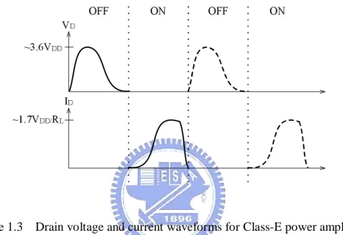
operating as a switch driven by the input signal at the operating frequency. The ideal Class-E PA has two conditions [3]. First, the drain voltage is zero at the switching instants. Second, the first derivative of the drain voltage is zero when the active device turns on. The first condition prevents dissipation of the energy stored by the shunt capacitor at turn on, while the second makes the circuit less sensitive to component, frequency and switching instants variations. The ideal efficiency is 100 percent. The RF choke provides a dc path to the supply and approximates an open circuit at RF. Cs and part of Ls form a series resonator tuned at fundamental frequency.
A fraction of Ls is needed together with the capacitor shunting the active device, Cp,
to meet the Class-E PA conditions. Figure 1.3 shows VD and ID waveform of the
Class-E PA. It shows that the peak drain voltage is approximately 3.6VDD, while the
peak drain current is roughly 1.7VDD/RL.
Figure 1.3 Drain voltage and current waveforms for Class-E power amplifier.
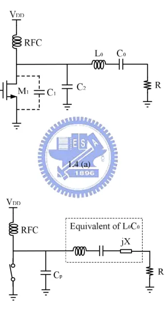
1.2.1 Ideal Class-E Power Amplifier
The brief concepts of the Class-E PA have discussed above. The more detail considerations of the Class-E PA will discuss in the subsequent sections. The Class-E PA had been first published in 1975s [4]. And the idealized operation of the Class-E tuned power amplifier was published in 1977s [5]. Figure 1.4 (a) and Figure 1.4 (b) shows the basic circuit and equivalent circuit of the Class-E power amplifier [5]. The Class-E PA includes a transistor operating as a switch, M1, a shunt capacitor, C2, an
RF choke, RFC, a series-tuned output circuit, L0C0, and the load resistor, R. C1 is the
parasitic capacitance in parallel at the switch including intrinsic transistor output capacitance and circuit stray capacitance.
1.4 (a)
1.4 (b)
Figure 1.4 (a) Basic circuit of the Class-E PA. (b) Equivalent circuit of the Class-E PA.
A simple equivalent circuit of the Class-E power amplifier is based on the following five assumptions [5].
•The RF choke only allows a dc current and has no series resistance.
•The quality factor of the series-tuned output circuit is high enough to make the
output current is mainly a sinusoid at the operating frequency.
•The switching action of the active device is instantaneous and lossless. The transistor
has zero saturation voltage, zero saturation resistance, and infinite off resistance. •The total shunt capacitance is independent of the drain voltage.
•The transistor can pass negative current and withstand negative voltage. (This is
inherent in MOS devices, but requires a combination of bipolar transistors and diodes.)
The series reactance jX is produced by the difference in the reactance of the inductor and capacitor of the series-tuned circuit. Note that the jX reactance applies only to the fundamental frequency, and it is assumed to be infinite at harmonic frequencies. The nominal component values for the idealized Class-E power amplifier are given by the following equations [5]:
out dd
P
V
R
2577
.
0
=
(1.1)
R
C
B
(
=
ω
P)
=
0
.
183
1
(1.2)X
(
=
ω
L
)
=
1
.
152
R
(1.3)1.2.2 Practical Considerations
The analysis presented in section 1.2.1 is based on several simple assumptions which are not always acceptable for practical and on-chip design. For examples [6]: •Non-ideal LC passive components
The loss of the on-chip passive components (mainly inductors) in CMOS technology is larger than the off-chip passive components.
•Large RF choke
It is hard to implement large RF choke in a single chip for on-chip design. •Nonzero transition time
Real transistors have nonzero transition times and, especially at high frequencies, it may cause a lot of loss.
Variations in component values, operating frequency, and duty cycle can have an effect on the performance of the Class-E PA [7].
•Nonzero ON resistance or nonzero saturation voltage •Finite loaded Q
The output current is not a pure sine wave, because the series-tuned output circuit has a finite loaded Q.
1.2.3 Finite DC-Feed Inductor
The Class-E PA has required a RF choke between the dc power supply and the active device in the previous description. But the RF choke itself is large in size, so it presents problems in terms of both large resistance loss and hard to implement in a single chip. Therefore, a smaller inductor is necessary for designing on-chip Class-E PA. However, using a finite dc-feed inductor instead of an RF choke in the Class-E PA has a number of benefits in the following [8].
•A small DC-feed inductor has lower loss due to a smaller series resistance.
•The cost and the chip size will decrease to make it implemented in a single chip
easier.
•The load resistance will also increase, thus making the design of the matching
Therefore, there is a strong interest to pursue the design of the Class-E PA with finite dc-feed inductor.
1.2.4 Cascode Topology
In order to overcome the low breakdown voltage of the active devices the cascode topology can be used in designing an on-chip Class-E PA. With the finite DC-feed inductor, the load resistance can be increased for the same output power and supply voltage to achieve higher efficiency. From (1.1), for further increase of the load resistance (R), it is agreeable to allow higher supply voltage (Vdd) because the load
resistance is proportional to the square of the supply voltage. As the technology scale down, however, the safe operating voltage will decrease and the supply voltage should be reduced in order not to stress the active devices. The voltage stress on the active device can be reduced by the cascode topology, so the load resistance could be increased by the supply voltage increasing [9].
Usually, the active device is switched from the gate as shown in Figure 1.5 (a), but the maximum voltage stress in the transistor is Vdrain,max which can be as high as 3.6
Vdd for an ideal Class-E PA, resulting in low supply voltage and small load resistance.
On the contrary, if the active device is switched form the source instead of the gate as shown in Figure 1.5 (b), the maximum voltage stress is reduced to Vdrain,max –VGG
because the source of the switching transistor swings up with the input voltage. Therefore, the maximum allowable supply voltage is Vdrain,max /( Vdrain,max –VGG) times
larger for common-gate switch than that for a simple common-source switch. In order to avoid presenting the input driving stage with a low impedance node, a common-source stage is combined with the common-gate switch into a cascode as shown in Figure 1.5 (c). This allows the supply voltage almost twice the value for a single common-source switch.
Figure 1.5 (a) Common-source. (b) Common-gate switch. (c) Common-gate switch combined with common-source stage into a cascode in order not to provide low-impedance load to the driving. (d) Maximum voltage stress is shown for each case assuming the input signal Vin swings from 0 V to VGG [9].
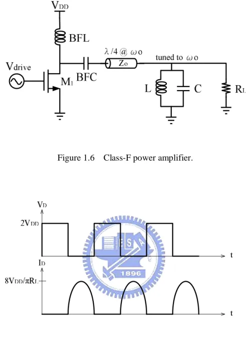
1.3 Class-F Power Amplifier
A suitable driver stage for lowering the input driver power in system level is very important. The Class-F PA is switched-mode PA with high efficiency, and it can shape the input waveform of the Class-E PA. Therefore, the Class-F PA is suitable for Class-E driver stage. The Class-F PA is shown in Figure 1.6 [6] [7]. The output tank is tuned to resonance at the operating frequency and is assumed to have a high enough Q to act as a short circuit at all frequencies outside of the desired bandwidth. The length of the transmission line is chosen to be precisely a quarter-wavelength at the operating frequency. At the operating frequency, the drain sees a pure resistance of RL=Zo, since the tank is an open circuit there, and the transmission line is therefore
terminated in its characteristic impedance. At the second harmonic of the operating frequency, the drain sees a short, because the tank is a short at all frequencies away from the operating frequency(and its modulation sidebands), so the transmission line now appears as a half-wavelength piece of line. Clearly, the drain sees a short at all even harmonics of the operating frequency, because the tank still appears as a short circuit; the transmission line appears as an odd multiple of a quarter-wavelength and therefore provides a net reciprocation of the load impedance. Drain voltage and current of the ideal Class-F PA shows in Figure 1.7.
Figure 1.6 Class-F power amplifier.
Figure 1.7 Drain voltage and current waveforms for Class-F power amplifier.
1.4 Polar Transmitter
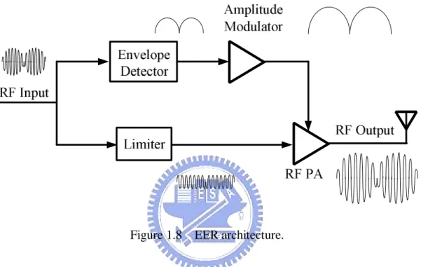
The polar transmitter with Class-E PA can be used for WiMAX of severe linearity requirement. One of the first applications of polar technique is Envelope Elimination and Restoration (EER), as shown in Figure 1.8 [10] [11] [12] [13]. The EER means
that the envelope of the RF input is eliminated by a limiter to generate constant envelope phase signal, and the magnitude information is extracted by an envelope detector. The envelope and phase signal are amplified separately and
Figure 1.8 EER architecture.
then recombined to restore the magnitude and phase information using a switched mode RF PA. Therefore, the envelope and phase signal can be recombined if the envelope of the RF output of a switched-mode RF PA is proportional to its supply voltage. And using a switched-mode PA is more efficient than using a linear PA. That is, the EER architecture can linearize the switched-mode RF PA without compromising efficiency. But the EER system still has some disadvantages. First, it has delay mismatch between the envelope and phase paths because the two paths employ different type of circuits and operating at different frequencies. It must be
maintain below as an acceptable level. Second, limiters incorporating active stages such as differential pairs exhibit a substantial AM-to-PM conversion effect at high frequencies. Third, envelope detector also introduces AM-to-AM conversion effect. Using the polar transmitter could solve second and third disadvantages of EER system. But the first disadvantage of EER is also the challenge of polar transmitter.
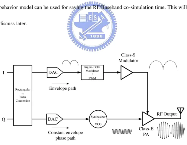
The polar transmitter, as shown in Figure 1.9 [10] [14], includes baseband DSP, DAC, amplitude modulator, phase modulator and switched mode RF power amplifier. The amplitude modulator includes a Sigma-Delta Modulator (SDM) or a Pulse Width Modulator (PWM) and a Class-S Modulator. The phase modulator includes a synthesizer or a Voltage Control Oscillator (VCO). And the switched-mode RF PA is Class-E power amplifier. The I/Q signals are split into the envelope signal and constant envelope phase signal. The constant envelope phase signal (RF) is applied at the gate of the transistor of the Class-E PA, and the envelope signal (low-frequency) directly modulates the supply of the Class-E PA. A high efficiency linear RF PA can be achieved by combining two paths. Finally, we can use the polar transmitter with Class-E PA to achieve high linearity and high efficiency at the same time. The polar transmitter does not use the envelope detector and a limiter, so it could solve the second and third disadvantages of EER system. But the first disadvantage of EER, timing synchronous between the envelope path and phase path, is still the challenge of
polar transmitter. And the second challenge of the polar transmitter is the wider bandwidth of the envelope signal and phase signal. Because of the wider bandwidth of envelope and phase signal, it has to increase the bandwidth of the two paths to introduce noise largely. It has trade-off between the signal bandwidth and noise. And the synchronization between the envelope signal and the constant envelope phase signal is very difficult. On the contrary, the traditional transmitters use the in-phase and quadrature-phase components so the synchronization is easier. That is why the traditional transmitters used more frequently than the polar transmitter. Finally, the behavior model can be used for saving the RF/Baseband co-simulation time. This will discuss later. Class-E PA Class-S Modulator RF Output `` Sigma-Delta Modulator / PWM DAC DAC Envelope path Constant envelope phase path Synthesizer / VCO I Q Rectangular to Polar Conversion
1.5 Organization
This thesis describes the design of on-chip RF CMOS Class-E PA.
Chapter 2 begins with the proposed Class-E PA consists of a cascode topology with finite dc-feed inductor and a Class-F driver to achieve an on-chip PA. Chapter 3 presents the implementation and experimental results including layout descriptions, measurement setup, and measurement results. Chapter 4 discusses the behavior modeling of the proposed Class-E PA for efficient RF/Baseband co-simulation. Chapter 5 makes conclusions and shows the future works.
Chapter 2
On-Chip RF CMOS Class-E Power
Amplifier Design
2.1 The Proposed Class-E Power Amplifier
The frequency range of the Class-E PA is 2.3~2.7GHz. The output power should be larger than 20dBm to meet the transmitter of the WiMAX Class-2 specifications. Figure 2.1 shows the proposed Class-E PA. The proposed on-chip Class-E PA consists of a cascode topology with finite dc-feed inductor and a Class-F driver to obtain higher efficiency and output power. The detailed analysis of this work shall be discussed in the subsequent sections.
Finite DC-Feed Inductor
Cascode
Tuned-Out Inductor Class-F
2.1.1 Cascode Topology
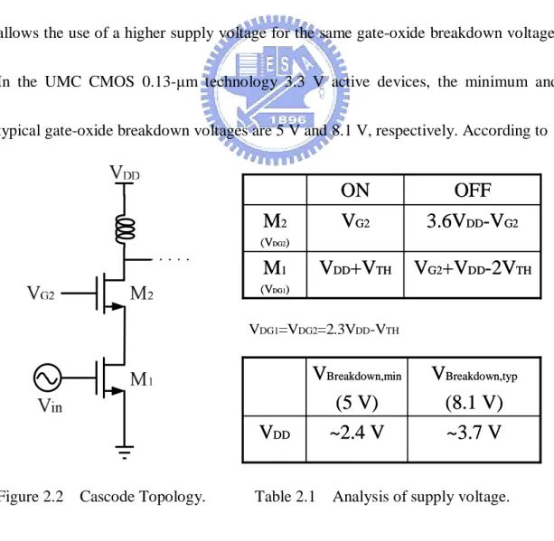
The design specifications include frequency range and output power. A supply voltage (VDD) should be determined in the beginning. Table 2.1 shows the maximum
VDG when the switching device is on and off respectively. Assume the supply voltage
of the Class-F driver equals to VDD, and the voltage stress on the M1 and M2 are the
same. We can obtain a maximum device stress of VDG1=VDG2=2.3VDD-VTH.
Compared with the conventional common-course topology allows approximately the twice supply voltage. In other words, cascode topology solution (VDG=4.6VDD-VTH),
allows the use of a higher supply voltage for the same gate-oxide breakdown voltage. In the UMC CMOS 0.13-μm technology 3.3 V active devices, the minimum and typical gate-oxide breakdown voltages are 5 V and 8.1 V, respectively. According to
V
G2+V
DD-2V
THV
DD+V
THM
1 (VDG1)3.6V
DD-V
G2V
G2M
2 (VDG2)OFF
ON
V
G2+V
DD-2V
THV
DD+V
THM
1 (VDG1)3.6V
DD-V
G2V
G2M
2 (VDG2)OFF
ON
VDG1=VDG2=2.3VDD-VTH~3.7 V
~2.4 V
V
DDV
Breakdown,typ(8.1 V)
V
Breakdown,min(5 V)
~3.7 V
~2.4 V
V
DDV
Breakdown,typ(8.1 V)
V
Breakdown,min(5 V)
the equation in Table 2.1, we can obtain an initial design parameter, VDD, of about 2.4
V. Now, we already have design parameters of operating frequency, supply voltage and output power. So we can start to obtain the other parameters of the Class-E PA.
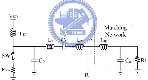
2.1.2 Finite DC-Feed Inductor
Based on equations (A.1) ~ (A.8), we can obtain the other passive component
parameters of the Class-E PA. Figure 2.3 shows the schematic of the Class-E PA with finite dc-feed inductor including the matching network.
Figure 2.3 Schematic of Class-E PA with finite DC-feed inductor. The Class-E PA specifications:
GHz f mW dBm P V Vdc =2.4 , out =24 ≈251 , =2.5
Table 2.2 Design parameters. Resonator tank:
Select the quality factor of the loading network is about 3
ω
Q
R
L
s=
⋅
(2.1) s sL
C
⋅
=
21
ω
(2.2)Table 2.3 Design parameters. Matching network [6]: Because R ≈27.7 Ω <RL =50 Ω So
=
−
1
R
R
R
X
L L m (2.3)1
−
=
R
R
R
X
L L Cm (2.4)Table 2.4 Design parameters.
2.1.3 Tuned-Out Indcutor
Base on cascode topology, efficiency could be improved by adding an inductor between M1 and M2 [3]. When M1 is turned off, is associated to charging and
discharging transients of the parasitic capacitor at node r, as shown in Figure 2.4, which is consist of M1 drain-bulk and drain-source capacitances and M2 source-bulk
and gate-source capacitances. This power loss is not negligible at all and may degrade the advantages of an increased supply voltage. An effective way to minimize this power loss contribution is tuning out the capacitive parasitics by means of an inductor, resonating Cr at the desired operating frequency. A blocking capacitor CBL is inserted
between the inductor and ground. The inductor provides the current charging the parasitic capacitance, minimizing the current flow through the active devices, and their power dissipation [3]. The cascode Class-E PA with tuned out inductor shows in Figure 2.5.
Figure 2.4 Cascode topology with tuned out inductor Lr.
Figure 2.5 The cascode Class-E power amplifier with tuned out inductor.
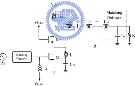
2.1.3 Class-F Driver
issue to shape the input waveform for turning the transistor on and off. To obtain the shortest transition time from one switching state to the other, a square waveform should be applied into the Class-E PA. This function can be realized by using the Class-F PA as a driver stage, which can generate appropriate harmonics of the input signals and combining them into a square waveform [15] [16]. The Class-F driver stage, as shown in Figure 2.6, is used to produce square waveform signal to drive the Class-E power amplifier. The two parallel-tuned LC circuits operate at first and the third harmonics resonance of the input frequency where the inductance values can be computed by (2.5) and (2.6). The LC resonators are used to eliminate the even harmonics while the first and third harmonics are passed to next stage. And in order to loose the demand on high driving power in the Class-E power amplifier, using an inductor Lt to tune out the parasitic capacitor at M1 gate [17].
1 2 1
1
:
1
C
L
harmonic
stω
=
(2.5) 3 2 39
1
:
3
C
L
harmonic
ndω
=
(2.6) whereω 2
=
π
f
Figure 2.6 Cascode Class-E PA with Class-F driver.
2.1.4 Summary
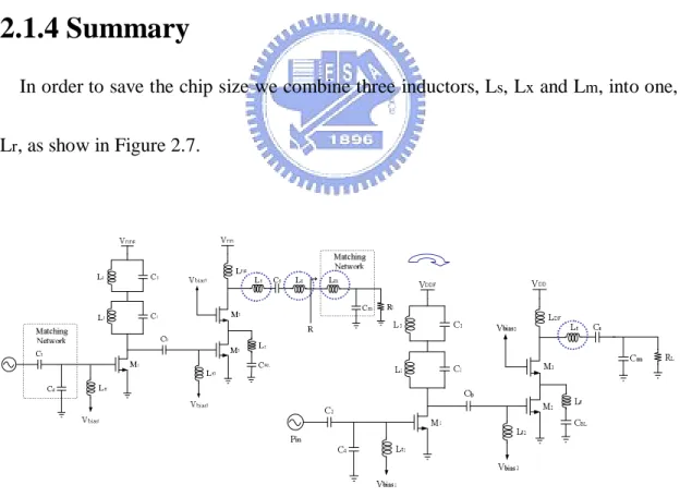
In order to save the chip size we combine three inductors, Ls, Lx and Lm, into one, Lr, as show in Figure 2.7.
2.2 Simulation Results
The simulation environment is on the cadence RFDE. And the simulation results
are listed below:
•Drain Voltage & Current of M1 & M2
100 200 300 400 500 600 700 0 800 -2 0 2 4 6 8 -4 10 -50 0 50 100 150 200 -100 250 time, psec Id 2 (m A ) V d 2 ( V ) Vd2 Id2 100 200 300 400 500 600 700 0 800 0.0 0.5 1.0 1.5 -0.5 2.0 0 50 100 150 -50 200 time, psec Id 1 (m A ) V d 1 ( V )
•Output Power & PAE v.s. Input Power -14 -12 -10 -8 -6 -4 -2 0 2 4 -16 6 18 19 20 21 17 22 40 45 35 50 Pin P o u t ( d B m ) P A E (% )
Freq = 2.5 GHz
Pout PAEFigure 2.9 Simulation results of output power and PAE v.s. input power.
•Output Power & PAE v.s. Operating Frequency
2.2 2.4 2.6 2.8 2.0 3.0 17 18 19 20 21 16 22 25 30 35 40 45 20 50 Freq, Hz P A E (% ) P o u t ( d B m )
Pin = -3 dBm
Pout PAE•Output Power & PAE v.s. Supply Voltage 1.0 1.5 2.0 2.5 3.0 0.5 3.5 5 10 15 20 0 25 0 20 40 -20 50 Vdd (V) P A E (% ) P o u t ( d B m )
Pin = -3 dBm
Freq = 2.5 GHz
Figure 2.11 Simulation results of output power and PAE v.s. supply voltage.
•LSSP (Large Signal S-Parameter)
1.0E9 2.0E9 3.0E9 4.0E9 5.0E9
0.0 6.0E9 -12 -10 -8 -6 -4 -2 -14 0 -12 -10 -8 -6 -4 -2 -14 0 RFfreq S (1 ,1 ) S (2 ,2 )
•Comparisons Parameters Tech. (CMOS) Operate Frequency (Hz) Die Area (mm^2) Supply Voltage (V) Output Power (dBm) PAE (%) Gain (dB) (Pin) FOM [17] 2006 Radio & Wireless 0.18µm 2.35G 1.7 1.2 11 44.5 5 (6) 0.10 [18] 2005 Microwave Con. 0.18µm 2.4 1.1*1.1 1.2 9.5 33 11 (-1.5) 0.21 Proposed Work (Po-Sim) 0.13µm 2.5G 1*1.49 3.3 21 48.4 24 (-3) 95.66
•FOM =Pout×Gain×PAE× f 2 (W×GHz2)
Chapter 3
Implementation and Measurement
Results
3.1 Chip Layout Descriptions
The experimental chips, P1 and P2, are designed and fabricated by UMC 0.13-μm single-poly-eight-metal (1P8M) CMOS technology. P1 is Class-E PA without Class-F driver and P2 is Class-E PA with Class-F driver. The total chip area include pads, as shown in Figure 3.1 and 3.2, are 1mm×1mm and 1mm×1.49mm. The total width of M1 and M2 are 2112 μm. In order to decrease the device cell numbers for layout easier,
we choose the maximum finger number and maximum width in one cell. Finally, M1
and M2 only need each 11 cells to achieve the total width of 2112 μm. The wider
metal lines are used in power line because of the large current through it. The triangular metal lines are used to average the large current to each cells of the active device for preventing the device broken when large current through it. Using the MOS capacitors in order to meet the rules of DRC metal density, and these MOS capacitors also could be the bypass capacitors used in each dc bias at the same time. To decrease
the chip size, we combine three inductors, Ls, Lx and Lm, into one, Lt, as shown in Figure 3.1 and 3.2. Gnd Gnd RFout Gnd Gnd RFin Vbias1 VDDE Vbias2 VDD Gnd Gnd Gnd
3.2 Measurement Results
3.2.1 Measurement Setup
The equipments used in this measurement are list below:
•Signal Generator (ESG) × 1 •Power Supply × 5 •Spectrum Analyzer × 1 •Oscilloscope × 1 •150μm GSG Probe × 2 •DC Probe (Single point) × 2 •DC Probe (6-pin, 150μm) × 1
Designing the circuit must consider the impedance matching, and the ESG, Spectrum Analyzer and Oscilloscope are required to examine the matching condition. However, the impedance of these equipments are 50Ω. The measurement setup shows in Figure 3.3.
G S G G S G 6 Pin DC Probe G S G G S G Power supply ESG Oscilloscope
Time domain waveform
Spectrum Analyzer
Frequency domain signal
DC
Power supply
DC
3.2.2 Simulation and Measurement Results
In the beginning, the DC measurement is performed. Unfortunately, a dc current is found at the gate of transistor M2, as shown in Figure 3.4. But M2 gate should not
have dc current. So, some debug works is done after measurement. The reasonable answer could be due to the gate leakage current of MOS bypass capacitor. Since the 1.2V MOS bypass capacitors are used at each dc bias nodes. However, the bias voltage of M2 gate is 2.1V that exceeding the 1.2 V, which may cause the gate-oxide
of the MOS bypass capacitor breakdown and produce leakage current at M2 gate.
Therefore, the circuit performances have severely degradation due to incorrect bias. The measurement results of the P1 are list below.
•M2 Gate Current v.s. M2 Gate Voltage
0.5 1.0 1.5 2.0 2.5 3.0 0.0 3.5 500 1000 1500 0 2000 Vg2 (V) Ig 2 (u A ) m1 m1 indep(m1)= plot_vs(Ig2, Vg2)=191.300 3.4 (a)
3.4 (b)
Figure 3.4 M2 gate leakage current of (a) simulation result (b) from UMC document [19].
•Output Power & Power Gain & PAE v.s. Input Power
-10 -8 -6 -4 -2 0 2 4 6 8 -12 10 -5 0 5 10 15 20 -10 25 Pin (dBm) P o u t (d B m ) 3.5 (a)
-10 -8 -6 -4 -2 0 2 4 6 8 -12 10 10 15 5 20 Pin (dBm) P o w e r G a in ( d B ) Simulation Measured 3.5 (b) -10 -8 -6 -4 -2 0 2 4 6 8 -12 10 10 20 30 40 0 50 Pin (dBm) P A E ( % ) 3.5 (c)
Figure 3.5 Simulation results of (a) output power v.s. input power (b) power gain v.s. input power (c) PAE v.s. input power.
•Pout & PAE v.s. Freq. 2.2 2.4 2.6 2.8 2.0 3.0 12 14 16 18 20 10 22 Frequency (GHz) P o u t (d B m ) Simulation Measured 3.6 (a) 2.2 2.4 2.6 2.8 2.0 3.0 10 20 30 40 0 50 Frequency (GHz) P A E ( % ) 3.6 (b)
Figure 3.6 Simulation results of (a) output power v.s. operating frequency (b) PAE v.s. operating frequency.
•Output Power & PAE v.s. Vdd 1.0 1.5 2.0 2.5 3.0 0.5 3.5 0 5 10 15 20 -5 25 Vdd (V) P o u t (d B m ) 3.7 (a) 1.0 1.5 2.0 2.5 3.0 0.5 3.5 -60 -40 -20 0 20 40 -80 60 Vdd (V) P A E ( % ) 3.7 (b)
Figure 3.7 Simulation results of (a) output power v.s. supply voltage (b) PAE v.s. supply voltage.
Chapter 4
Behavior Model
To do the RF/Baseband co-simulation of the proposed on-chip Class-E PA with polar transmitter the behavior model is needed. In order to reduce the time of circuit simulation and system verification, behavior models are used in circuit simulation and RF/Baseband co-simulation.
4.1 Behavior Model of Class-E PA
In the modeling flow from [20], the RF modules can be divided into three parts: input interface, output interface and Gm stage. We developed the behavior models of
each part. Then circuit simulation and system simulation will be accomplished by these behavior models. In this chapter, the behavior model of Class-E PA without driver stage is for efficient and accurate RF/Baseband co-simulation. The modeling flow starts form the impedance networks and the switched-mode transistor.
•Capacitor
Figure 4.1 (a) shows the capacitor model in UMC design kits documents and Figure 4.1 (b) is it equivalent circuit. The capacitor can be represented by series R, L and C. Figure 4.2 shows the s-parameter simulation results of the behavior model and transistor level. L L2 R= L=78 pH C C5 C=3.85 pF R R5 R=1.24 Ohm 4.1(a) [21] 4.1(b) Figure 4.1 Capacitor of (a) UMC model (b) it equivalent circuit.
2 4 6 8 0 10 -0.5 0.0 0.5 -1.0 1.0 freq, GHz re a l( S (1 ,1 )) 2 4 6 8 0 10 -0.8 -0.6 -0.4 -0.2 -0.0 -1.0 0.2 freq, GHz im a g (S (1 ,1 ))
•Inductor
Figure 4.3 (a) shows the inductor model in UMC design kits documents and Figure 4.3 (b) is it equivalent circuit. The inductor can be represented by series R and L with parallel C. Figure 4.4 shows the s-parameter simulation results of the behavior model and transistor level.
L L5 R= L=791 pH C C10 C=38 fF R R9 R=1.36 Ohm 4.3 (a) [21] 4.3(b) Figure 4.3 Inductor of (a) UMC model (b) it equivalent circuit.
2 4 6 8 0 10 -0.8 -0.6 -0.4 -0.2 -0.0 -1.0 0.2 freq, GHz re a l( S (1 ,1 )) 2 4 6 8 0 10 0.2 0.4 0.6 0.8 0.0 1.0 freq, GHz im a g (S (1 ,1 ))
•Input Matching
Figure 4.5 (a) and (b) shows the schematic and equivalent circuit of input matching. Similarly, use the method above the behavior model of input matching can be achieved by capacitors, inductors and resistances. Figure 4.6 shows the s-parameter simulation results of the behavior model and transistor level.
L l2 R= L=60 pH C C2 C=0.79 pF R r6 R=1.24 Ohm R r3 R=0.62 Ohm C c3 C=3.254 pF C C6 C=600 f F R r5 R=1.24 Ohm L l1 R= L=78 pH R r7 R=86.3458 Ohm C C1 C=3.75 pF C C7 C=250 fF L L3 R= L=791 pH R R1 R=1.36 Ohm Pin RL LDF Lt Cs Cm Lr CBL C2 C1 Lt2 Vbias1 M1 M2 Vbias2 VDD 4.5 (a) 4.6 (b)
Figure 4.5 Input matching of (a) schematic (b) it equivalent circuit.
2 4 6 8 0 10 -0.5 0.0 0.5 -1.0 1.0 freq, GHz re a l( S (1 ,1 )) 2 4 6 8 0 10 -0.8 -0.6 -0.4 -0.2 -0.0 0.2 -1.0 0.4 freq, GHz im a g (S (1 ,1 ))
Figure 4.6 SP simulation results of the input matching of behavior model and transistor level.
•Output Matching
Figure 4.7 (a) and (b) shows the schematic and equivalent circuit of input matching. Similarly, use the method above the behavior model of output matching could be achieved by capacitors, inductors and resistances. Figure 4.8 shows the s-parameter simulation results of the behavior model and transistor level.
Pin RL LDF Lt Cs Cm Lr CBL C2 C1 Lt2 Vbias1 M1 M2 Vbias2 VDD C C12 C=40 fF C C16 C=1.25 pF C C11 C=40 fF C C15 C=10 fF C C13 C=40 fF L l3 R= L=30 pH C C9 C=0.12 pF R r8 R=1.24 Ohm C C14 C=209 fF L L5 R= L=2.42 nH R R3 R=2.92 Ohm R r7 R=86.3458 Ohm C C7 C=250 fF R r10 R=10 kOhm C C10 C=3.75 pF R R2 R=3.3 Ohm L L4 R= L=2.92 nH R r9 R=1.24 Ohm L l4 R= L=78 pH 4.7 (a) 4.7(b)
Figure 4.7 Output matching of (a) schematic (b) it equivalent circuit.
2 4 6 8 0 10 -0.5 0.0 0.5 -1.0 1.0 freq, GHz re a k( S (2 ,2 )) 2 4 6 8 0 10 -0.5 0.0 0.5 -1.0 1.0 freq, GHz im ag (S (2 ,2 ))
Figure 4.8 SP simulation results of the output matching of behavior model and transistor level.
4.1.2 Switched-Mode Transistor
Vdrain Vgate Vsupply Vin Vout V_DC Vbias2 Vdc=Vgg2 V NetlistInclude NetlistInclude1 UsePreprocessor=yes IncludeFiles[6]=core_rf_v112.lib.scs tt IncludeFiles[5]=L130E_HS12_V241.lib.scs tt IncludeFiles[4]=pad_rf_v112.lib.scs typ IncludeFiles[3]=mimcaps_rf_v112.lib.scs typ IncludeFiles[2]=io_rf_v112.lib.scs tt IncludeFiles[1]=l_cr20k_rf_v111.lib.scs typ IncludePath= /home/dada/RFDE/UMC013FDK/Models/Spectre NETLIST INCLUDE SwitchV SWITCHV1 V2=1.9 V R2=1.05 Ohm V1=- 1 V R1=12 kOhm Model=SWITCHVM1 V R R1 R=0.1 Ohm R r3 R=0.62 Ohm C c3 C=3.254 pF UMC013DADA_NEWClassE_tune_M1_schematic X1 C c6 C=3.2 pF V_DC Vbias1 Vdc=Vgg1 V SwitchV_Model SWITCHVM1 AllParams= V2=1.0 V R2=1.0 MOhm V1=0.0 V R1=1.0 Ohm V V_DC SRC4 Vdc=Vdd V VtSine SRC5 Phase=0 Damping=0 Delay=0 nsec Freq=BW MHz Amplitude=1.63 V Vdc=1.63 V P_1Tone PORT1 Freq=RFfreq P=dbmtow(Pin) Z=50 Ohm Num=1 I_ProbeIbias1 I_ProbeIbias2
I_Probe Isupply I_Probe Iout Term Term2 Z=50 Ohm Num=2 P_1Tone PORT2 Freq=RFfreq GHz P=polar(dbmtow(0),0) Z=50 Ohm Num=2 I_Probe Iin V_DC SRC3 Vdc=3.3 V Pin RL LDF Lt Cs Cm Lr CBL C2 C1 Lt2 Vbias1 M1 M2 Vbias2 VDD Pin RL LDF Lt Cs Cm Lr CBL C2 C1 Lt2 Vbias1 M1 M2 Vbias2 VDD
Figure 4.9 Using ADS switch mode to be the switched-mode transistor model.
Because the operation of the transistor M1 is like a switch, it can not be modeled by
a simple Gm stage. Hence, we use the switch model provide in ADS at first. Figure
4.10 shows the design procedure of the switched-mode transistor. Here, we have three thresholds, 0.3 V, 0.8 V and 1.8 V. When Vgg1 < 0.3 V and 0.8V < Vgg1 < 1.8 V, the
ADS switch can be used to model it, as shown in Step 1. When Vgg1 > 1.8 V, the
resistance equation in triode-region MOSFET can be used to model it, as shown in Step 2. When 0.3 V < Vgg1 <0.8 V, we modify the parameter in step 1 to fit it, as
shown in Step 3. Finally, we combine Step1 ~ Step 3, as shown in Step 4, to accomplish the behavior model of the switch-mode transistor. The comparisons of circuit simulation are shown in Figure 4.11.
-1 0 1 2 -2 3 100 200 300 400 0 500 Vgg1 Id ( m A ) -1 0 1 2 -2 3 100 200 300 400 0 500 Vgg1 Id ( m A ) Step 1. Step 3. Step 4. Step 2. -1 0 1 2 -2 3 100 200 300 400 0 500 Vgg1 Id ( m A ) ) ( 1 TH GS ox n on V V L W C R − = µ -1 0 1 2 -2 3 100 200 300 400 0 500 Vgg1 Id ( m A ) 0.3 0.8 1.8 *Three thresholds *Four regions
100 200 300 400 500 600 700 0 800 2 4 6 8 10 0 11 time, psec V d ( V ) 100 200 300 400 500 600 700 0 800 -50 0 50 100 150 200 250 -100 300 time, psec Id ( m A ) -4 -2 0 2 4 6 8 -6 10 14 16 18 20 12 22 Pin P o u t ( dB m ) -4 -2 0 2 4 6 8 -6 10 20 30 40 10 50 Pin P A E ( % ) 1.0 1.5 2.0 2.5 3.0 0.5 3.5 -20 0 20 40 -40 60 Vdd P A E ( % ) RMSE = 3.17 % Transistor Level Behavior Model
2.2E9 2.4E9 2.6E9 2.8E9
2.0E9 3.0E9 30 35 40 45 25 50 RFfreq P A E ( % )
Figure 4.11 Comparisons of circuit simulation between transistor level and behavior model.
4.2 RF/Baseband Co-Simulation
a three-port circuit, as shown in Figure 4.12. In order to do RF/Baseband co-simulation a simplified polar transmitter is presented, as shown in Figure 4.13. And the behavior model used in RF/Baseband co-simulation excludes the transistor M2. Figure 4.14 shows the schematic of behavior model without transistor M2. Because of RF/Baseband co-simulation in transistor level costs a lot of time, more the half month. Therefore, instead of using real passive components from UMC FDK model, inductors and capacitors, the ideal passive components in ADS to do RF/Baseband co-simulation. In other words, only the switched-mode transistor behavior model is used in RF/Baseband co-simulation.
Pin RL LDF Lt Cs Cm Lr CBL C2 C1 Lt2 Vbias1 M1 M2 Vbias2 VDD Class-E PA Class-S Modulator RF Output `` Sigma-Delta Modulator / PWM DAC DAC Envelope path Constant envelope phase path Synthesizer / VCO I Q Rectangular to Polar Conversion Three-port circuit
RF_Signal RF_Signal RF_Signal RF_Signal
RF_Signal
Push into Info to read loc al information
Note: Rate_ID Modulation RS -CC 0 BPSK 1/2 1 QPSK 1/2 2 QPSK 3/4 3 16QAM 1/2 4 16QAM 3/4 5 64QAM 2/3 6 64QAM 3/4
Uplink Transmitter EVM Measurement WMAN OFDM:
WMAN_OFDM_UL_TxEVM.dsn
WMAN UL Signal Source RF
MeasEqn Meas1 samplingrate=RF_SamplingRate Eqn M eas VSA_89600_1_Sink V2 SamplesPerSymbol=0.0 TStep=0 sec VSATitle="Simulation output" VSA VAR Calculation SS3_stop=stop_SS3 SS3_start=start_SS3 SS2_stop=stop_SS2 SS2_start=start_SS2 SS1_stop=stop_SS1 SS1_start=start_SS1 Eqn Var WMAN_UL_Constellation_RF Constellation2 FrameDuration=Continuous DL_Ratio=0.5 FrameMode=FD D stop=SS2_stop start=SS2_start Bandwidth=Bandwidth Rate_ID=Rate_ID DataLength=DataLength NumberOfSS=NumberOfSS RIn=DefaultRLoad
ULConst ellat ion
WM AN WMAN_UL_Constellation_RF Constellation3 FrameDuration=Continuous DL_Ratio=0.5 FrameMode=FDD stop=SS3_stop start=SS3_start Bandwidth=Bandwidth Rate_ID=Rate_ID DataLength=DataLength NumberOfSS=NumberOfSS RIn=DefaultRLoad
ULConst ellat ion
WM AN WMAN_UL_Constellation_RF Constellation1 FrameDuration=Continuous DL_Ratio=0.5 FrameMode=FDD stop=SS1_stop start=SS1_start Bandwidth=Bandwidth Rate_ID=Rate_ID DataLength=DataLength NumberOfSS=NumberOfSS RIn=50 Ohm
ULConst ellat ion
WM AN DF DF DefaultTimeStop=100 msec DefaultTimeStart=0 usec VAR Measurement_VARs FramesToAverage=20 Eqn Var VAR VAR2 RF_SamplingRate=floor(Bandwidth*n/8000+0.5)*8000* 2^int(OversamplingOption)
n=if(0==fmod(Bandwidth,1750000)) then 8.0/7 elseif(0==fmod(Bandwidth,1500000)) then 86.0/75 elseif(0==fmod(Bandwidth,1250000)) then 144.0/125 elseif(0==fmod(Bandwidth,2750000)) then 316.0/275 elseif(0==fmod(Bandwidth,2000000)) then 57.0/50 else 8.0/7 endi
Eqn Var VAR Signal_Generation_V ARs FCarrier=2507 MHz Bandwidth=4 MHz OversamplingOption=2 Rate_ID={1,1,1} DataLength={500,1000,2000} NumberOfSS=3 Eqn Var CxToPolar C10 WMAN_DataPattern RandomBits DataLength=DataLength[SSWithFEC] Pattern=PN 9 010001 WM AN
Dat aPat t ern
CxToTimedIQ C12 TStep=1/RF_SamplingRate i q TimedIQToCx T2 i q PM_Mod P2 Phase=0 Sensitivity=180/pi Power=dbmtow(7) FCarrier=FCarrier FloatToTimed F4 TStep=1/RF_SamplingRate GainRF G2 GComp="0 0 0" GCSat=1 PSat=1 W dBc1out=dbmtow(31) TOIout=3 W GCType=dBc1 NoiseFigure=0 Gain=dbpolar(6,0) EnvOutSelector O1 OutFreq=FCarrier SpectrumAnalyzerResBW RF ResBW =30 kHz Window =none Stop=DefaultTimeStop Start=DefaultTimeStart RLoad=50 Ohm Plot=Rectangular ResBW WMAN_EVM W5 FramesToAverage=FramesToAverage AverageType=RMS (Video) RLoad=D efaultRLoad WM AN W MAN_OFDM_UL_TxEVM_Info Information W MAN 802.16-2004
Design Information NetlistIncludeNetlistInclude1
UsePreprocessor=yes IncludeFiles[6]=core_rf_v112.lib.scs tt IncludeFiles[5]=L130E_HS12_V241.lib.scs tt IncludeFiles[4]=pad_rf_v112.lib.scs typ IncludeFiles[3]=mimcaps_rf_v112.lib.scs typ IncludeFiles[2]=io_rf_v112.lib.scs tt IncludeFiles[1]=l_cr20k_rf_v111.lib.scs typ IncludePath= /home/dada/RFDE/UMC013FDK/Models/Spectre NETLIST INCLUDE FloatToTimed F1 TStep=1/R F_SamplingRate W MAN_UL_SignalSrc W MAN_UL_SignalSrc Power=SignalPower MAC_Header={0XA2, 0X48, 0X22, 0X4F, 0X93, 0X0E} PilotPN_Phase=PilotPN_Phase IdleInterval=IdleInterval CyclicPrefix=CyclicPrefix Bandwidth=Bandwidth OversamplingOption=OversamplingOption BSID=BSID FrameNumber=FrameNumber UIUC=UIUC TimeOffset=TimeOffset PrmlTimeShift=PrmlTimeShift MidambleRepetition=MidambleRepetition SubchannelIndex=SubchannelIndex Subchannelization=Subchannelization Rate_ID=Rate_ID DataLength=DataLength SSW ithFEC=SS WithFEC NumberOfSS=NumberOfSS BB UL Source WM AN UMC013D ADA_ClassE_5_schematic_symbol UMC013D ADA_ClassE_5_schematic_symbol1 FCarrier1=FCarrier MTS=1/RF_SamplingRate V o u t V s u p p ly V in
Figure 4.13 Schematic of simple polar transmitter in ADS.
Behavior Model exclude M2
Vg1 Vdrain Vdc asc ode Vs upply Vout Vin Class E_PA5 Class E_PA1 Cm=0.332e-12 Lm=0.778e-9 Lx =1.38e-9 Cs =0.5e-12 Ls =7.5e-9 Ldf=2.3e-9 rpad2=86.3458 Cpad2=0.25e-12 l7=0.03e- 9 r 7=1.24 C7=0.12e-12 l6=0.078e-9 r 6=1.24 C6=3.75e-12 c 5=0.06e-12 r 5=3.3 L5=2.92e-9 c 4=0.05e-12 r 4=2.92 L4=2.42e-9 Cposim3=0.04e-12 Cposim2=0.165e- 12 Cposim1=0.872e- 12 c3=0.6e-12 r3=1.3 L3=0.7e-9 l2=0.02e-9 r2=1.24 C2=0.43e-12 l1=0.078e-9 r1=1.24 C1=2e- 12 rpad1=86.3458 Cpad1=0.25e-12 R2_mid=1.05 R1_mid=12e3 Vth2_mid=1.9 Vth1_mid=-1 Vth_high=1.8 Vth_mid=0.8 Vth_low=0.3 L=0.34e- 6 W=2114e-6 uCox=120e-6 Vth=0.524 Cp=3.2e- 12 Cgs =3.254e-12 Rs=0.1 Rg=0.62 R2=0.1 R1=6e6 Vth2=2.1 Vth1=- 1.4 s Vg1 out Vd d d2 d in Netlis tInclude Netlis tInclude1 Us ePreprocess or=yes Inc ludeFiles[6]=c or e_rf_v 112.lib.s cs tt Inc ludeFiles[5]=L130E_HS12_V241.lib.scs tt Inc ludeFiles[4]=pad_r f_v 112.lib.s cs typ Inc ludeFiles[3]=mimcaps _rf_v112.lib.sc s typ Inc ludeFiles[2]=io_r f_v 112.lib.s cs tt Inc ludeFiles[1]=l_cr 20k_rf_v111.lib.s cs ty p Inc ludePath= /home/dada/RFDE/UMC013FDK/Models /Spec tre
NETLIST INCLUDE Ter m Ter m2 Z=50 Ohm Num=2 P_1Tone PORT2 Freq=RFfreq GHz P=polar(dbmtow(0),0) Z=50 Ohm Num=2 V_DC Vbias 2 Vdc=2.1 V I_Pr obe Ibias2 V_DC SRC4 Vdc=Vdd V VtSine SRC5 Phase=0 Damping=0 Delay =0 ns ec Freq=BW MHz Amplitude=Vam V Vdc =3.3 V I_Pr obe Is upply
UMC013DADA_Class E_1_sc hematic
X3 I_Pr obe Idcasc ode V_DC SRC3 Vdc =3.3 V V_DC Vbias1 Vdc =Vgg1 V I_Pr obe Ibias 1 I_Pr obe Iout I_Probe Iin P_1Tone PORT1 Fr eq=RFfr eq P=dbmtow(Pin) Z=50 Ohm Num=1 Pin RL LDF Lt Cs Cm Lr CBL C2 C1 Lt2 Vbias1 M1 M2 Vbias2 VDD Pin RL LDF Lt Cs Cm Lr CBL C2 C1 Lt2 Vbias1 M1 M2 Vbias2 VDD
The simulation results of RF/Baseband co-simulation are shown in Figure 4.15. The conditions are 14 MHz bandwidths and 2.5GHz carrier frequency. Three different modulation signals are considered in the RF/Baseband co-simulation. The results show the root-mean-squared error (RMSE) is about 0.125 dB.
RF/Baseband Co-Simulation -16.5 -16 -15.5 -15 -14.5 -14 16QAM 1/2 QPSK 1/2 64QAM 2/3 RMSE = 0.125 dB E V M ( d B ) Transistor Level Behavior Model
Figure 4.15 Comparisons of RF/Baseband co-simulation.
4.3 Comparisons of Simulation Time
After finishing the circuit simulation and RF/Baseband co-simulation, the
simulation time comparisons are presented. Figure 4.16 shows the comparisons of the circuit simulation time, the simulation time of the proposed behavior model are less than transistor level. Figure 4.17 shows the comparisons of the simulation time of the RF/Baseband co-simulation, the behavior model could save about 93% simulation
time compared with the transistor level. Therefore, the proposed behavior model could save a lot of simulation time.
15.25 0.28 25.75 0.57 45.25 0.62 93.67 0.95 219.14 3.75 290.63 6.2 0 50 100 150 200 250 300
HB HB_Pin HB_Vdd HB_Freq TRAN LSSP Transistor Level
Behavior Model
Figure 4.16 Comparisons of circuit simulation time.
174926.1 12445.42 0 50000 100000 150000 200000 Transistor Level Behavior Model S im u la ti o n T im e ( S ec o n d s)
Chapter 5
Conclusions and Future Works
5.1 Conclusions
This thesis presents an on-chip Class-E PA implemented in UMC 0.13-µm CMOS technology. Instead of the RF choke, the proposed design uses the finite dc-feed inductor technique for suitable implement in a single chip. In order to obtain higher output power, increasing the supply voltage (VDD) by the cascode topology is
successful. The efficiency could be improved by tuning out the parasitic capacitor between two transistors, M1 and M2. The proposed Class-E PA achieves power added
efficiency (PAE) of 48.4 % while delivering 21 dBm output power with the input driving power of -3 dBm at 2.5 GHz. In the design band, 2.3 GHz ~ 2.7 GHz, PAE is still above 44 %. The simulation time of RF/Baseband co-simulation could be reduced about 93% by the proposed behavior model.
5.2 Future Works
For the future works, the behavior model of the Class-E PA can be further
the effect of the loading network of the Class-E PA on polar transmitter to try to find out what kind of loading network of Class-E PA is suitable for polar transmitter.
Appendix 1
Analysis of Ideal Class-E PA with
Finite DC-Feed Inductor
In [22], one of the first attempts was made to study finite dc-feed inductor. Some other relevant papers include [23] [24]. All these papers have something in common, the procedure of obtaining final circuit component values is either long, complex and iterative, and doesn’t provide a direct insight into the circuit design, or is too simplistic and not exactly. Practically, the design of the Class-E PA with finite dc-feed inductor is a transcendent problem from the mathematical point of view. Therefore, the designer needs to iteratively figure out the system of equations for a certain set of input parameters to gain the final circuit component values. If any of the input parameters is changed, the calculation must be repeated from the beginning. Thus, it is a tedious and extremely impractical procedure. The [8] propose another approach to this problem. The system of transcendent equations is numerically solved for a certain number of discrete points of an input parameter, and the obtained results are interpolated by the Lagrange polynomial. The polynomial interpolation provides adequate accuracy and can be used for any value of the input parameter on that
segment, if it performs with enough density of points on the segment of interest. In other words, it obtains clear and directly usable design equations for the Class-E PA. The design parameters of the Class-E PA have presented in equations (1.1), (1.2) and (1.3). These equations are base on the Lck is RF choke. But in case of the Class-E
PA with finite dc-feed inductor, these equations don’t hold anymore [8]. At the beginning of the design procedure, the designer could choose a value of inductance that he would like to use for the finite dc-feed inductor. Therefore, the reactance of this inductor is known, and it is given by
ck
dc
L
X
=
ω
(A.1)On the other hand, an ideal Class-E PA provides a 100% DC-to-RF efficiency. Therefore, the DC resistance that the circuit presents to the supply source is also known from the PA specifications, and is simply given as
out dd dc
P
V
R
2=
(A.2) Depending on the dc dc R Xratio, the circuit parameters R, B and X will change their value from those given in equations (1.1), (1.2) and (1.3) for the RF choke based Class-E PA. These three parameters have calculated by numerically solving the transcendent circuit equations for a number of different values of
dc dc
R X
ratio. The results of these calculations are given in Table A.1 [8].
Table A.1 Class-E PA elements as function of the dc dc R X ratio [8].
Figure A.1 Effect of the finite DC-feed inductor on the Class-E PA elements [8].
In order to obtain explicit design equations for the Class-E PA component values, [8] have used the Lagrange polynomial interpolation of the numerically obtained results. Finally, the new equations for Class-E power amplifier with finite dc-feed inductor are presented in the following equations.
If 1< (=z)<5 R X dc dc , ) 01397 . 0 1754 . 0 7783 . 0 979 . 1 ( 2 3 2 z z z P V R out dc − + − = (A.3) ) 01672 . 0 1881 . 0 7171 . 0 229 . 1 ( 1 2 3 z z z R B= − + − (A.4) ) 03894 . 0 4279 . 0 591 . 1 202 . 1 ( z z2 z3 R X = − + − + (A.5) If 5< (= z)<20 R X dc dc , ) 10 707 . 5 002812 . 0 04805 . 0 9034 . 0 ( 2 5 3 2 z z z P V R out dc − + − ⋅ − = (A.6) ) 10 893 . 2 001426 . 0 02429 . 0 3467 . 0 ( 1 2 5 3 z z z R B= − + − ⋅ − (A.7) ) 10 587 . 7 003794 . 0 006641 . 0 6784 . 0 ( z z2 5z3 R X = + − + ⋅ − (A.8)
Design equations (A.3)~(A.8) are explicit, relatively simple and can be used for any value of
dc dc
R X
z= within the corresponding segment. But outside these segments, they are not valid.
The utilization of a finite dc-feed inductor has several major benefits. First, it results in a higher load resistance in comparison to the case of RF choke. This effect makes the design of low-loss matching networks easier, since the designer typically needs to transform a standard 50 Ohm termination to the load resistance of several
Ohms. Furthermore, the excessive inductance X is also lower, and the shunt susceptance B is increased. This increase of the shunt susceptance is particularly useful, as it extends the maximum frequency limitation of the device imposed by its output capacitance.
Appendix 2
Behavior Model of Switched-Mode
Transistor
•Step 1 – Ideal switch in ADS
ON Resistance -1 0 1 2 -2 3 100 200 300 400 0 500 Vgg1 Id ( m A ) Transistor Level Behavior Model
Figure A.2 Simulation results and Verilog-A code of step 1. •Step 2 – Modify ON resistance at region of 0.3(V) < Vgg1 < 0.8(V),
-1 0 1 2 -2 3 100 200 300 400 0 500 Vgg1 Id ( m A ) Transistor Level Behavior Model ) ( 1 TH GS ox n on V V L W C R − = µ
Figure A.3 Simulation results and Verilog-A code of step 2. •Step 3 –Modify ON resistance at region of Vgg1 > 1.8(V), where Vgg1 is Vbias1
-1 0 1 2 -2 3 100 200 300 400 0 500 Vgg1 Id ( m A ) Transistor Level Behavior Model
•Step 4 – Combine step 1, step 2 and step 3 -1 0 1 2 -2 3 100 200 300 400 0 500 Vgg1 Id ( m A ) Transistor Level Behavior Model RMSE = 0.003 mA
Bibliography
[1] Thomas H. LEE, “The Design of CMOS Radio-Frequency Integrated Circuits,” second edition, Cambridge University Press 1998.
[2] Frederick H. Rabb, Peter Asbeck, Steve Cripps, Peter B. Kenington, Zoya B. Popovich, Nick Pothecary, John F. Sevic and Nathan O. Sokal, “RF and Microwave Power Amplifier and Transmitter Technologies – Part 2,” High Frequency Electronics, May 2003.
[3] Mazzanti, A.; Larcher, L.; Brama, R.; Svelto, F., ”Analysis of Reliability and Power Efficiency in Cascode Class-E PAs,” Solid-State Circuits, IEEE Journal of Volume 41, Issue 5, May 2006 Page(s):1222–1229
[4] N.O Sokal and A.D. Sokal, “Class E-A new class of high-efficiency tuned single-ended switching power amplifiers,” IEEE, JSSC, vol. SC-10, pp. 168-176, June 1975.
[5] FREDERICK H. REBB, “Idealized Operation of the Class E Tuned Power Amplifier,” IEEE, Transactions on Circuits and Systems, Vol. 24, pp. 725-735, Dec. 1977.
[6] Mihai Albulet, “RF Power Amplifiers,” Noble Publishing Corporation, 2001. [7] Raab, F. H. “Effects of Circuit Variations on the Class E Tuned Power
Amplifier,” IEEE JSSC, vol. SC-13 (April 1978): 239-247.
[8] D. Milosevic, J. van der Tang and A. van Roermund, “Explicit Design Equations for Class-E Power Amplifiers with Small DC-feed Inductance,” Circuit Theory and Design, 2005. Proceedings of the 2005 European Conference on Volume 3, 28 Aug.-2 Sept. 2005 Page(s):III/101 - III/104 vol. 3
[9] C. Yoo and Q. Huang, “A Common-Gate Switched 0.9-W Class-E Power Amplifier with 41% PAE in 0.25-μm CMOS,” JSSC, vol. 36, no. 5, May 2001. [10] B. Razavi, “RF Microelectronic,” NJ, USA: Prentice-Hall PTR, 1998.
Restoration,” Proc. IRE, Vol.40, pp. 803-806, July 1952.
[12] D. Su and W. Sander, “An IC for Linearizing RF Power Amplifiers Using Envelope Elimination and Restoration,” IEEE JSSC, Vol. 31, pp. 2252-2258, Dec. 1998.
[13] H. L. Kraus, C. W. Bostian, and F. H. Raab, “Solid State Radio Engineering,” John Wiley & Sons, Inc., 1980.
[14] Nagle, P.; Burton, P.; Heaney, E.; McGrath, F.; “A Wide-Band Linear Amplitude Modulator for Polar Transmitter Based on the Conpect of Interleaving Delta Modulation,” Solid-State Circuits, IEEE Journal of Vol. 37, Issue 12, Dec.2002 Page(s):1748-1756.
[15] C.C. Ho, C.W. Kuo, C.C. Hsiao, Y.J. Chan, “A Fully Integrated Class-E CMOS Amplifier with a Class-F Driver Stage,” IEEE RFIC Symposium, June 2003. [16] P. Luengvongsakorn, A. Thanachayanon, “A 0.1-W CMOS class-E power
amplifier for Bluetooth applications,” Digital Object Identifier, Page(s): 1348-1351 Vol.4, TENCON 2003.
[17] H.S. Oh, T. Song, E. Yoon, C.K. Kim, “A Power-Efficient Injection-Locked Class-E Power Amplifier for Wireless Sensor Network,” IEEE Microwave and Wireless Components Letters, vol. 16, no. 4, April 2006.
[18] Munir M. El-Desouki, M. Jamal Deen and Yaser M. Haddara, “A Low-Power CMOS Class-E Power Amplifier for Biotelemetry Applications,” Microwave Conference, 2005 Oct. European
[19] UMC Design Kits document, L130E_HS12_V241.pdf
[20] C. D. Hung, W. S. Wuen, Mei-Fen Chou, and Kuei-Ann Wen, “A Unified Behavior Model of Low Noise Amplifier for System-Level Simulation,” accepted by European Conference on Wireless Technology (ECWT 2006), Manchester, UK, Sep. 2006.
[22] R.E. Zulinski and J.W. Steadman, “Class E Power Amplifiers and Frequency Multipliers with Finite DC-Feed Inductance,” IEEE Trans. Circuits and Systems, vol. CAS-34, no. 9, pp. 1074-1087, September 1987.
[23] D.K. Choi and S.I. Long, “Finite DC Feed Inductor in Class E Power Amplifiers-A Simplified Approach,” 2002 IEEE MTT-S Microwave Symposium Digest, vol. 3, pp. 1643-1646, June 2002.
[24] M. Iwadare and S. Mori, K. Ikeda, “Even Harmonic Resonant Class E Tuned Power Amplifier without RF choke,” Electronics and Communications in Japan, Part 1. vol.79, no. 1, 1996.
Vita
姓名 : 吳家岱 性別 : 男 籍貫 : 桃園縣 生日 : 民國七十二年四月三十日 地址 : 桃園縣龍潭鄉中興村中興路 388 號 學歷 : 國立交通大學電子工程研究所碩士班 2005/09~2007/06 私立中原大學電機工程學系 2001/09~2005/06 桃園國立陽明高級中學 1998/09~2001/06論文題目 : RF CMOS Class-E Power Amplifier Design
![Figure 1.2 shows the circuit schematic of the Class-E power amplifier [1] [2]. The dc current flowing through the RF choke (L ck ) is modulated by the power device (M 1 ), operating as a switch driven by the input signal at the operating frequency](https://thumb-ap.123doks.com/thumbv2/9libinfo/8422943.180641/16.892.190.742.219.700/schematic-amplifier-current-flowing-modulated-operating-operating-frequency.webp)