Effects of Postdeposition Annealing on the Characteristics of
HfO
xN
yDielectrics on Germanium and Silicon
Substrates
Chao-Ching Cheng,aChao-Hsin Chien,a,b,zChing-Wei Chen,aShih-Lu Hsu,b Chun-Hui Yang,band Chun-Yen Changa
a
Institute of Electronics, National Chiao-Tung University, Hsinchu, Taiwan 300, China
bNational Nano Device Laboratory, Hsinchu, Taiwan 300, China
We have systematically investigated the impact that postdeposition annealing共PDA兲 has on the physical and electrical properties of HfOxNythin films sputtered on Ge and Si substrates. These two substrates display contrasting metal-oxide-semiconductor
characteristics that we attribute to the different compositions of their interface layers 共ILs兲. We observed an increased GeO2 incorporation into the HfOxNydielectric and severe volatilization of the IL on Ge after higher PDA processing. These undesired
phenomena in the HfOxNy/Ge gate stacks may be responsible for their different electrical properties with respect to those of the
HfOxNy/Si gate stacks, i.e., a further scaling of the capacitance-equivalent thickness, a significant presence of fixed positive
charges and electron-trapping sites, and a degradation of dielectric reliability. In addition, the anomalous low-frequency-like behavior of the high-frequency capacitance–voltage curves in inversion for the Ge capacitors was predicted from theoretical calculations.
© 2006 The Electrochemical Society. 关DOI: 10.1149/1.2203097兴 All rights reserved.
Manuscript submitted November 22, 2005; revised manuscript received February 14, 2006. Available electronically May 23, 2006.
The rapid advancement of complementary metal oxide semicon-ductor 共MOS兲 integrated circuit technologies during the past few decades has forced the Si-based microelectronics industry to face several huge technological challenges and to test some theoretical limits. Consequently, many novel device structures and materials have been proposed and are being explored eagerly in an effort to alleviate the tremendous scaling pressure required to improve device performances. High-permittivity共high-k兲 materials will probably be introduced as alternative gate dielectrics, in place of ultrathin con-ventional SiO2or oxynitrides, in light of leakage concerns and reli-ability issues. Meanwhile, substrate engineering, e.g., pseudomor-phic SiGe channels grown on the Si substrates for p-type field effect transistors共FETs兲1 and strained Si channels on the relaxed graded SiGe buffer layers for n-type FETs,2is being pursued to enhance the carrier mobility in the channel also. Inspired by the advanced progress in the development of high-k dielectrics in Si-based metal oxide semiconductor field effect transistor共MOSFET兲 applications, increasingly attention is being focused on the feasibility of integrat-ing high-k gate dielectrics with Ge because of its intrinsically higher mobility than Si. To date, the superior electrical properties of several high-k metal oxides deposited on the Ge substrate have been dem-onstrated, including ZrO2,3HfO2,4,5 and Al2O3.6It has been sug-gested that surface pretreatment with SiH47or NH38prior to depo-sition of these metal oxides is required to obtain high-quality gate dielectrics on Ge substrates. In this paper, we describe our study into the physical and electrical characteristics of sputtered HfOxNy thin
films deposited onto bulk Ge and conventional Si substrates. The incorporation of nitrogen into HfO2gate dielectrics cannot only in-crease the crystallization temperature but also strengthen immunity toward oxygen diffusion and resistance toward boron penetration without lowering the dielectric constant.9Apart from the poor inter-face quality that results from the presence of nitrogen, HfOxNyfilms
are expected to have advantages over HfO2in regard to some other essential properties. HfOxNy has improved thermal stability with
respect to those of surface-nitrided and top-nitrided HfO2because the nitrogen atoms exist in the bulk dielectric and at the dielectric-Si interface. Several investigators have reported Si-based MOSFETs possessing Hf-oxynitride gate dielectrics.9-11 Nevertheless, funda-mental differences exist between the thermochemical properties of not only the Ge and Si substrates but also their oxides.12Clearly, the implication is that each interface layer 共IL兲 formation process, as well as the nature of the interactions at the surface, might possess
quite different features during post-thermal treatment. Indeed, the starting surface of these two substrates is a critical parameter in determining both the final thickness of a HfO2film grown through physical vapor deposition 共PVD兲 and the IL formed.13 The bulk properties of high-k films deposited on Ge substrates also might be different from those on Si substrates. This study was an attempt to clarify these concerns through a comprehensive comparison of the physical and electrical characteristics of HfOxNy/Ge and HfOxNy/Si systems; in this paper we discuss the impact that postdeposition annealing共PDA兲 has on both the high-k dielectric and the interfacial compositions on Ge and Si substrates.
Experimental
共100兲 Ga-doped p-type Ge wafers having a resistivity of 25–29⍀ cm and 共100兲 p-type Si wafers having a resistivity of 1–10⍀ cm were used. All the wafers were subjected to a cleaning process involving several cycles of sequential rinsing with deionized 共DI兲 water followed by dipping in HF acid solution 共DI water/HF, 1:30兲. After N2drying, HfN thin films were first deposited through reactive sputtering in an Ar + N2 ambient 关N2/Ar + N2= 0.33兴 with a 99.9% pure Hf target. During deposition, the chamber pres-sure was 7.6 mTorr and the sputtering power was 150 W. In an attempt to suppress any additional oxidation, which can help to minimize the thickness of IL, the following PDA was performed to convert HfN into HfOxNy in an N2 ambient rather than an O2 ambient.9 The samples were split into many groups so that PDA could be performed at different temperatures共400, 500, and 600°C兲 and various durations共1, 3, and 5 min兲 to study their impact on the interfacial characteristics of the HfOxNygate dielectrics on both the Ge and Si substrates. Next, a 1000 Å thick layer of platinum共Pt兲 was deposited using electron-beam evaporation through a shadow mask to pattern the capacitor electrode. Postmetallization annealing 共PMA兲 was then performed at 400°C for 30 s. The capacitance area was evaluated through optical microscopy of the circular capacitor dots. Finally, aluminum共Al兲 was deposited on the back side of the wafer, followed by sintering in the forming gas共N2/H2, 90:10兲 at 300°C for 30 min.
High-resolution transmission electron microscopy共HRTEM兲 was employed to characterize the thicknesses and interfacial structures of the Hf-oxynitride films on both the Ge and Si substrates before and after PDA. The compositions and chemical bondings of the HfOxNy
films were analyzed using angle-resolved X-ray photoelectron spec-troscopy 共AR-XPS兲 with an Al K␣ radiation source operating at 1486.6 eV for excitation. Photoelectrons were collected at two take-off angles共30 and 60° with respect to the surface horizontal兲 and the z
binding energy was calibrated from the Pt 4f7/2 peak at 71.20 eV. The element depth profiles of these films were analyzed through Auger electron spectroscopy共AES兲 using Ar+ ion sputtering; the LM2 and MN2 transitions were used for germanium and hafnium, respectively, while KL1 transition was used for both nitrogen and oxygen. For characterization of electrical properties, capacitance-voltage 共C-V兲 and conductance-voltage 共G-V兲 curves were mea-sured using an HP4284 LCR meter. The gate leakage characteristics were measured using a Keithley 4200 semiconductor analyzer sys-tem.
Results and Discussion
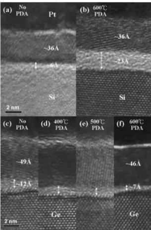
Physical characterization.— HRTEM images.— Figure 1a and b displays cross-sectional HRTEM images of the HfOxNy-sputtered films on the Si substrates before and after N2PDA. As expected, an additional IL growth appeared on the Si substrate after annealing at 600°C for 5 min. By contrast, we observed that the thickness of the IL between the HfOxNy dielectric and the Ge substrate did not
in-crease upon increasing the PDA temperature; indeed, it shrank somewhat, as illustrated in Fig. 1c-f. After PDA at 600°C, the IL thickness in the HfOxNy/Si increased from ca. 6 to ca. 23 Å; in contrast, that in the HfOxNy/Ge decreased from ca. 12 to ca. 7 Å.
Such shrinking after rapid thermal annealing in an N2ambient has also been observed for a HfO2/Ge gate stack.14We propose two possible causes for this phenomenon:共i兲 bond breaking in the IL, which leads to subsequent desorption, or共ii兲 densification of the IL; the mechanisms are discussed in further detail below. Even so, from the viewpoint of performance, we were gratified to observe the oc-currence of such contraction of the IL on the Ge system because aggressive equivalent oxide thickness共EOT兲 scaling may be more readily achieved. On the other hand, irrespective of the PDA
condi-tions, the thickness of the HfOxNy film on the Ge substrate was
larger than that on the Si substrate. This tendency is different from that reported by Kita et al. for the case of a sputtered HfO2film;13 they demonstrated that both the HfO2film and the IL were thinner on the Ge substrate than those on the Si substrate. We suspect that these contradictory findings might arise from the use of different oxidizing gases during sputtering.
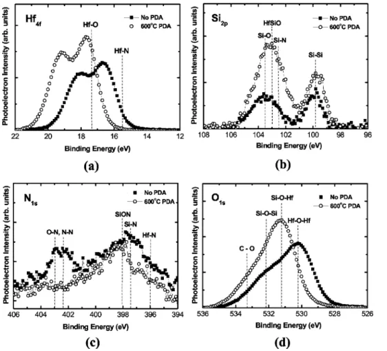
XPS and AES depth profiles.— Figure 2a-d displays the AR-XPS spectra of Hf 4f, Si 2p, N 1s, and O 1s, respectively, of the HfOxNyfilm on the Si substrate before and after PDA at 600°C. In this case, the take-off angle was 60°. The peak for the Hf 4f7/2 binding energy of the as-deposited film appeared at 16.70 eV with spin-orbital splitting 共SOS兲 of 1.5 eV; no additional components corresponding to metallic Hf appeared. When compared with the reported values of the binding energies for Hf–N 4f7/2 共15.55 ± 0.25 eV兲 and Hf–O 4f7/2共17.35 ± 0.20 eV兲,15-18our result indicates that a considerably large component of the as-deposited HfN film has been oxidized during deposition, even though N2was used as the only feed gas. Moreover, the peak in the Hf 4f7/2 spec-trum shifted toward higher binding energy after the subsequent PDA at 600°C for 5 min. The value of the binding energy for this peak is even higher than that of Hf–O binding; this finding reflects the fact that high-temperature annealing can further eliminate Hf–N bonds and lead to the formation of Hf–O–Si chemical bond. This high binding energy can be explained by considering the enhanced charge transfer from oxygen to hafnium and silicon.19-21Further evidence to support this argument is present in the Si 2p spectra. The as-deposited film displays a pronounced oxidized peak at a binding energy that is 3.7 eV higher than that of the Si substrate peak; this finding verifies the fact that a thin IL exists between the high-k dielectric film and the Si substrate. Moreover, this oxidized Si peak shifted slightly toward a lower binding energy, corresponding to Hf–O–Si bonding, with enhanced intensity after PDA at 600°C.21,22 The N 1s spectrum confirmed that the reduction of nitrogen had also occurred. The content of Si–N and Hf–N bonds obviously decreased after annealing, and the signals for N–O bonds and/or N2molecules also reduced significantly. These results imply that the residual oxy-gen in an N2 ambient plays important roles during annealing: it is able to replace nitrogen, bond to Hf atoms, and consequently leave residual SiNxas the major nitrogen-related mode of bonding.23,24In addition, the O 1s peak also shifted toward higher binding energy, concomitant with an enhanced intensity. Again, this result is closely related to the degree of Hf–O–Si bond formation. Based on these experimental data, we believe that the main composition of the IL of the as-deposited film was SiOxNy; the further increase in IL thick-ness, as observed from the TEM results, arises from the formation of an additional Hf-silicate layer after high-temperature processing.
As stated earlier, increasingly greater efforts are being devoted to the deposition and study of the properties of high-k films on Ge substrates;25,26detailed material analyses using XPS, however, re-main quite rare. Figure 3 presents the Hf 4f spectra of the HfOxNy
films on the Ge substrate with respect to the PDA temperature; the inset displays the O 1s core-level spectra for the as-deposited and 600°C PDA films. As the PDA temperatures and times increased, well-resolved Hf 4f spectra共i.e., an increasing ratio of the intensities of the Hf 4f5/2and Hf 4f7/2peaks兲 appeared that gradually approxi-mated that of pure Hf–O bonding. The dielectric film obtained after annealing at 600°C for 5 min exhibited a Hf 4f7/2peak energy of 17.1 eV and a branch ratio of 0.75, coinciding with the ideal core-level degeneracy. Similar to HfOxNy deposited on the Si substrate, oxygen can readily substitute for nitrogen to be the first nearest neighbor of an Hf atom and, consequently, cause the deposited film to transform into a near-stoichiometric HfO2film. The asymmetric energy band in the O 1s spectrum共inset兲 is likely to arise from the IL, which probably contained GeOx 共x ⬉ 2兲 or the Hf–Ge mixed
oxide. Unfortunately, overlapping of the Ge LMN Auger signal with the O 1s core level makes it impossible to identify the exact contri-bution of each of these chemical species, but from the variation in
Figure 1. HRTEM images of sputtered HfOxNythin films on共a, b兲 Si and
共c–f兲 Ge substrates before and after PDA. 共a兲 Si: No PDA; 共b兲 Si: PDA at 600°C;共c兲 Ge: no PDA; 共d兲 Ge: PDA at 400°C; 共e兲 Ge: PDA at 500°C; and 共f兲 Ge: PDA at 600°C. The PDA time for all annealed samples was 5 min.
intensity in the O 1s spectrum we conclude that no other chemical bonding exists for oxygen after high-temperature thermal process-ing; this finding indicates that subsequent growth of an additional intermediate layer between HfOxNyand the Ge substrate, as we had
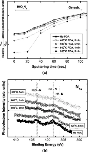
observed for the HfOxNy/Si system, did not proceed. Figure 4a pre-sents a profile, obtained through AES, of the ratio of the NKL1/OKL1 atomic concentration as a function of the sputtering time. The trend of a declining NKL1/OKL1 concentration ratio suggests that upon increasing the PDA temperature and duration, the substitution of nitrogen atoms by oxygen atoms became more significant in the HfOxNydielectric. Figure 4b presents the corresponding N 1s
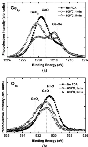
spec-tra. From its peak intensity, Ge–N bonding appears to be the main type of bonding; it is accompanied by a very small number of Hf–N bonds. Upon increasing the PDA temperature we observed decreases in the intensities of both the Hf–N and Ge–N bonds; this finding seems to be closely related to the decomposition of these bonds in a high-temperature ambient. As discussed earlier, Hf–N bonds can be replaced by Hf–O bonds during the sputtering process; in contrast, the reported dissociation temperatures for Ge–O, Ge–N, Si–O, and Si–N bonds are ca. 360, 490, 740, and⬎1000°C, respectively,27 suggesting that Ge–N bonds are less stable than Si–N bonds. Our experimental results are consistent with the previous report: the most obvious reductions in intensity of the Ge–N peak occurred at annealing temperatures above 500°C. As mentioned earlier, we be-lieve that one of the possible reasons for the shrinkage of the IL is bond breakage, but our preliminary evidence suggests that it is too early to draw any conclusions. Because of the lower stabilities of Ge-related chemical species, however, it seems reasonable to specu-late that a correlation exists between IL dissociation and shrinkage. To obtain more evidence to support our hypothesis, we used AES and AR-XPS to perform further analyses of Ge-related bonding. Figure 5a displays the AES depth profiles of the Ge/Hf ratio with respect to the annealing temperature. A clear incremental accumula-tion of Ge toward the dielectric surfaces occurred upon increasing the PDA temperature. Secondary ion mass spectroscopy共SIMS兲 was used recently to detect the significant diffusion of Ge elements into HfO2films that had been deposited either at 485°C through metal-lorganic chemical vapor deposition共MOCVD兲 or subjected to PDA at 550°C.28Taking into consideration the resulting AR-XPS spectra for Ge 2p共Fig. 5b兲 allows us to further understand the chemical bonding states of the incorporated Ge atoms. Because Ge 2p spectra are more surface-sensitive than Ge 3d core-level spectra, as a result of the extremely reduced inelastic mean free path共IMFP; ca. 8 Å in our case兲 for photoelectrons having low kinetic energies,29we used
Figure 2. 共a兲 Hf 4f, 共b兲 Si 2p, 共c兲 N 1s, and共d兲 O 1s core-level spectra of HfOxNy
thin films on Si substrates before and after PDA at 600°C共 = 60°兲. The PDA time was 5 min.
Figure 3. Hf 4f core-level spectra of HfOxNythin films on Ge substrates
before and after PDA under various conditions. 共Inset兲 O 1s spectra 共 = 60°兲.
them to study the changes in the composition of the high-k dielectric film on the Ge substrate that occurred during the PDA. The results of a previous report30regarding the spectra of oxidized Ge 2p al-lowed us to assign the peaks corresponding to elemental Ge, GeO, and GeO2 at 1217.6, 1219.1, and 1220.6 eV, respectively; these peaks are marked in the figure. Initially, no Ge-related chemical species appeared within the high-k dielectric, but once PDA had been performed, we observed that the intensity of the signal for GeO2 increased upon increasing both temperature and annealing time. The AR-XPS spectra in Fig. 5c indicate that the intensity of the signal for GeO2increased when the take-off angle was changed from 30 to 60°. This finding suggests that more GeO2was incorpo-rated into the upper portion of the gate dielectric, which is similar to the AES examination. The volatilization sources as well as the chemical form of Ge during diffusion process are still in debate and fervently discussed.31,32There are two possible mechanisms respon-sible for the GeO2incorporation into HfOxNy thin film: one is
dif-fusion of Ge atom from the dissociated IL and/or substrate itself, which is then oxidized by the incoming residual oxygen; the other is the subsequent oxidation of a volatile product such as GeO, formed as a result of the same origins, caused by residual oxygen during annealing. No matter which of these mechanisms is correct, we be-lieve the out-diffusion can be achieved through the grain boundaries of the crystallized high-k film. Thus, we believe that the dissociation of the IL is the real cause of the shrinkage, rather than densification,
because of the detection of GeO2 within the bulk of the high-k dielectric. Further discussion for this identification is presented in the next section.
XPS-ultrathin HfON layer on Ge.— For more-direct characteriza-tion of IL desorpcharacteriza-tion on the Ge substrate, we deposited an ultrathin HfOxNy film. Because the IL formed inherently during the initial
sputtering stages, we manipulated the sputtering time to deposit the bulk dielectric共i.e., HfOxNy兲 as thin a layer as possible. The
inter-esting changes that occurred to the Ge 2p and O 1s AR-XPS spectra before and after PDA at 600°C are presented in Fig. 6a and b,
Figure 4. 共a兲 Variation of relative NKL1/OKL1 atomic concentration as a function of the sputtering time and the PDA conditions.共b兲 N 1s core-level spectra of HfOxNythin films on Ge substrates before and after PDA under
various conditions共 = 60°兲.
Figure 5. 共a兲 Variation of relative GeLM2/HfMN2atomic concentration as a function of the sputtering time and the PDA conditions.共b兲 Ge 2p core-level spectra of HfOxNythin films on Ge substrates before and after PDA under
various conditions 共 = 30°兲. 共c兲 Angle-resolved Ge 2p spectra of these samples.
respectively. Apart from the Ge substrate signals in Fig. 6a, the IL of the no-PDA film exhibited a broad band having its main peak at 1219.7 eV; this feature is likely to result from a mixture of GeOxNy
and HfOxNy. Because high-temperature annealing at 893°C is ca-pable of forming the tetragonal Hf1−xGexO2structure, that upon fur-ther heating to 1200°C yields scheelite HfGeO4phase,33 strongly suggesting poor intermixing and alloying in Ge and Hf systems. The IL peak after annealing at 600°C moved closer to the value expected for GeO2. This result provides evidence for the dissociation and oxidation of the Ge–N bonds. Another noteworthy feature is that the ratio of the peak intensities of this broad peak and that of the Ge substrate deceased with increasing both the temperature and time; this result indicates implicitly that the thickness of the IL was re-duced after annealing. To obtain a quantitative description of the IL shrinkage process, we assumed that the Ge 2p spectrum was com-posed simply of two components: GeOx共x ⬉ 2兲 and Ge. From this
assumption, we calculated the thickness of the IL in the as-deposited sample to be ca. 9.5 Å using a GeOx/Ge ratio of 1.3 and an IMFP of
ca. 8 Å.34After annealing at 600°C for 1 and 5 min, the IL thick-nesses decreased to ca. 7.9 and 4.5 Å, respectively. These values confirm that the IL does undergo certain chemical changes during high-temperature processing. Because the Hf 4f spectrum shifted 共not shown兲 in a manner similar to that of the thick film discussed earlier but with lower intensity because of the ultrathin layer, we believe these out-diffused species escaped into the air. Ogino and Amemiya proposed several possible mechanisms for the loss of Ge.35Three possible reactions are the following35,36
GeO共s兲 → GeO共v兲 关1兴
Ge共s兲 + GeO2共s兲 → 2GeO共v兲 关2兴
2Ge共s兲 + O2共v兲 → 2GeO共v兲 关3兴
First, perhaps the GeO chemical species directly transforms into gaseous GeO.37Second, the chemical reduction of GeO2into vola-tile GeO has been characterized at temperatures ranging from 350 to 550°C.12,38-40Thus, PDA at 600°C should accelerate desorp-tion rate through these mechanisms. Third, considering the ready oxidation of Ge, mechanism 3 is likely to occur during annealing. It also implies that the entire exposed Ge substrate as well as the top Ge surface with HfOxNycovering are probably oxidized by residual
oxygen in an N2ambient. It is reasonable to suspect that the result-ant higher GeO2concentration near the top of thicker HfOxNyfilm is intimately related to gaseous GeO diffusion from the back side and sidewall of Ge substrate.41With additional XPS measurements, we did observe that the surface of high-k/Si samples were contami-nated with GeO2when they were annealed alongside the high-k/Ge samples in an N2ambient above 500°C共not shown here兲. Thus, we cannot exclude the possibility that the presence of higher GeO2 con-centration near the surface might result from the further oxidation of airborne GeO in the chamber. However, in our case of ultrathin HfOxNyfilm, we found that the resultant peak intensity in the O 1s
spectrum, presented in Fig. 6b, decreases with increasing annealing time after PDA at 600°C; the longer the time, the more significant was the out-diffusion of GeOx. This fact implies that the amount of GeO2 arising from gaseous GeO diffusion from the back side and sidewall of Ge substrate is limited in our case; in other words, it only plays a minor role with respect to the volatilization processes. As a result, we thought that the GeO2detected inside the bulk of the thicker HfOxNy film probably arose mainly from further oxidation
of GeO from the IL and top Ge surface during annealing.
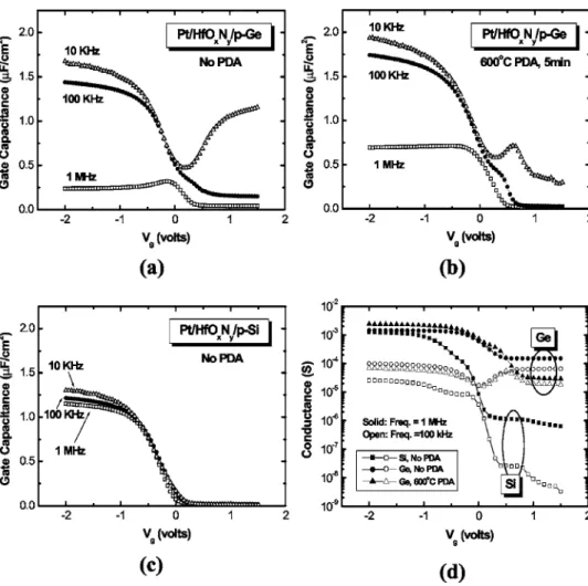
Electrical characterization.— C-V and G-V properties.— Figure 7a-d presents the multifrequency C-V and G-V characteristics of the HfOxNy/p-Ge and HfOxNy/p-Si MOS capacitors, respectively. For
the as-deposited HfOxNy film on the Ge and Si substrates, we
ob-serve two noteworthy features: one is that the frequency dispersion at the accumulation region of HfOxNy/Ge is more obvious than that of the HfOxNy/Si, and the other is that the frequency dispersion at the inversion region is unique for the capacitors on the Ge substrate. The dispersion effects at both regions are apparently reduced after annealing at 600°C. Here, we estimated the frequency dispersion in the accumulation simply from the differences between the 1 MHz and 100 kHz curves at Vg= −2 V. We obtained a value of only 8% for the as-deposited HfOxNy/Si; in contrast, it was as high as 82%
for the as-deposited HfOxNy/Ge and it decreased to 41% after PDA
at 600°C. As far as the frequency dispersion of the accumulation capacitance is concerned, the series resistance共Rs兲, which is
depen-dent on the bulk wafer resistivity and the contact resistances, can be the dominated mechanism; its effect will be amplified with the mea-sured conductance共Gm兲.42Nevertheless, the Ge substrates that we
used had slightly higher bulk resistivity than that of Si, together with the same accumulation Gmmeasured at 1 MHz. Thus, the effect of Rs only partly explains the difference between the dispersions of
these two capacitor systems. In other experiments, we found that larger frequency dispersions also existed when depositing ZrOxNyor
Hf-silicate high-k films onto the Ge substrate, relative to those on the Si substrate, when using Al or Pt metal gates共not shown here兲. Wu et al. reported that a large frequency dispersion of accumulation capacitance existed in high-k/Ge capacitors with NH3passivation, which was significantly improved by using the SiH4annealing in-stead of NH3pretreatment.7We may conclude that the dispersion behavior in the accumulation region is strongly related to the inter-face quality, e.g., the amount of the existing defects, before and after the annealing.
We clearly observed the anomalous low-frequency-like behavior of the high-frequency共in the kHz range兲 C-V curves in inversion for the capacitors on the Ge substrate but not on the Si substrate.
Simi-Figure 6.共a兲 Ge 2p and 共b兲 O 1s core-level spectra of ultrathin HfOxNythin
films on Ge substrates before and after PDA under various conditions共 = 60°兲.
lar phenomena have been explored by several groups, who attributed them to the fast rate of minority carrier generation in Ge.43 To clarify this behavior, we undertook a theoretical prediction model of the minority carrier response in the semiconductor. It is well known that two major mechanisms are responsible for the buildup of inver-sion charge, or the so-called generation current density, Jgen:共i兲 the thermal generation of electron/hole pairs via the trap levels within the space charge region共scr兲, denoted as Jscr, and共ii兲 the diffusion of minority carriers from the bulk substrate across the scr, denoted as Jdiff. For low-frequency-like behavior to emerge, the value of Jgen arising from these two contributions, Jscrand Jdiff, must be greater than the required displacement current 共Jdisp兲 flowing through the oxide. While under strong inversion, the following equations de-scribe these relations44
Jgen= Jscr+ Jdiff=eniw mir + eni2 1 Nmaj
冑
Dmir mir 关4兴 Jdisp= CoxdVg dt 艋 Jgen 关5兴 feff⬇ dVg/dt Voc 艋 Jgen CoxVac 关6兴 where e is the electronic charge, niis the intrinsic carrier concentra-tion, w is the scr width, and Nmajis the majority carrier concentra-tion; Dmirand mirare the diffusion coefficient and the generation lifetime of the minority carriers, respectively. The oxide capacitance Coxcan be approximated as being equal to the accumulation capaci-tance; Vacis the applied ac voltage. Table I lists all of the parameters used in our calculations; among them, the natural difference in ni between Si and Ge is the governing factor. For the Si substrate, themagnitude of Jscr, which is on the order of 10−9A/cm2, obviously dominates at room temperature because the magnitude of Jdiffis on the order of 10−12A/cm2. In comparison, even though the value of Jscrfor Ge increases to the order of 10−7A/cm2, as a result of the larger value of ni, the value of Jdiffincreases drastically to the order of 10−4A/cm2. The fact that J
diff, rather than Jscr, becomes the ma-jor component for Ge is predictable from the lower energy gap. Dimoulas et al. reported that the activation energy Eact extracted from the Arrhenius plot of the inversion conductance was ca. 0.66 eV for a temperature above ca. 45°C.45This value of Eact is close to the Ge bandgap at room temperature, suggesting that a greater fraction of the minority carrier originates from Jdiff, rather than from Jscr. We define an effective frequency fefffor the occur-rence of low-frequency-like behavior; the values correspond to ca. 0.01 Hz and ca. 2 kHz for Si and Ge, respectively. That is to say, the sufficiently high value of feffin Ge leads to the observed minority carrier response in the C-V characteristics, even in the kilohertz
Figure 7. Multifrequency共a兲–共c兲 C-V and 共d兲 G-V characteristics of Pt/HfOxNy/p
-Ge and Pt/HfOxNy/p-Si MOS capacitors
before and after PDA at 600°C.
Table I. Material and electrical parameters at 300 K used in the calculations.44,51 Si Ge Rs共⍀ cm兲 1–10 25–29 Nmaj共cm−3兲 5⫻ 1015 1⫻ 1014 ni共cm−3兲 1⫻ 1010 2⫻ 1013 w共m兲 0.41 1.16 Dmir共cm2s−1兲 40 100 mir共s兲 8⫻ 10−5 5⫻ 10−3 Cox共F/cm2兲 1.25 1.5 Vac共mV兲 50 50
regime, which is consistent with our experimental findings. In addi-tion, the reduced frequency response of the inversion capacitance after PDA may be explained in term of the minority generation lifetime. The high-temperature step assists to eliminate the process-induced bulky defects in the Ge substrate and thus, increases the value ofmiras well as lowers the rate of generation of the minority carrier.
Evaluating the measured capacitance Cmand conductance Gmat
strong inversion led to a minority carrier response time共R兲 of ca. 10−6for the Ge system; this value is 3 orders of magnitude shorter than that共ca. 10−3兲 of the Si system. As a result of the shorter value ofRfor Ge, an inversion layer is formed rapidly in response to an external ac signal at the gate; this result agrees well with our theo-retical predictions. The detailed calculation processes and basic as-sumptions are available in Ref. 45; in addition, we note that the contribution from the generation/recombination of e/h pairs through the interface states is excluded in the calculations because a hump appears in the HfOxNy/Ge system after annealing at 600°C,
indicat-ing the generation of some additional interface states. The interface state density 共Dit兲 at the midgap, as determined using Hill’s method,46is 4⫻ 1012cm−2. At this level of D
itwe should observe a larger frequency dispersion in inversion, but our experimental result conflicts with this prediction. Thus, we believe that the contribution of the value of Dit plays only a very minor role in the frequency dispersion in the Ge case, even though this factor may be critical in the Si case.
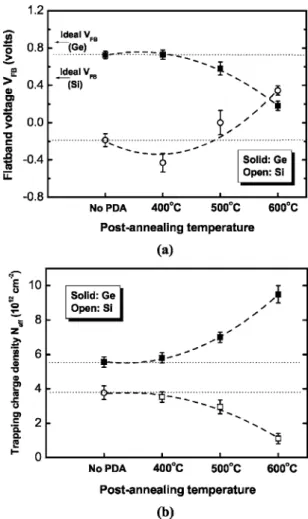
Oxide charge trapping and gate leakage current.— To correctly elucidate the effect of postannealing on the underlying shift in VFB, we carefully chose the maximum and minimum gate biases in the bi-directional C-V sweeps to avoid significant charge trapping. In-terestingly, we observe opposing trends in the VFBshift for these two gate stacks共Fig. 8a兲. Upon increasing the annealing temperature, the value of VFBof HfOxNy/Si undergoes a positive shift, whereas that of HfOxNy/Ge exhibits a negative shift. As far as the charges of
high-k film deposited on Si substrates are concerned, nitrogen-induced positive charges have been reported as being present in HfOxNysystems, relative to the charges of the pure metal oxides.11 The presence of positive fixed charges leads to the lowered value of VFB in the as-deposited HfOxNy film on the Si substrate. Similar
results have been presented for other nitrogen-incorporated metal oxides, e.g., ZrOxNy47 and TaOxNy.48The subsequent N2 PDA is expected to eliminate the bond imperfections, such as dangling bonds, nitrogen-related defects, and oxygen vacancies, thereby com-pensating for the positive charges in the dielectric film and returning VFBto its ideal value. We deduce that the bond repairing and charge neutralization processes also occur reasonably in the HfOxNy/Ge system. In fact, the continuing negative shift in the value of VFB upon increasing the PDA temperature departs from its ideal value. This deviation suggests that the value of VFBin HfOxNy/Ge may be driven not only by the mechanisms above but also by a certain predominant mechanism unobserved and/or inhibited in HfOxNy/Si. In addition to the differences in VFB, we also observe in Fig. 8b opposing dependences of the oxide charge trapped density共Neff兲 with respect to the PDA temperature for these two MOS structures. The value of Neff, i.e., the electron trap, is evaluated quantitatively by measuring the hysteresis width at VFB.49 We observe that the PDA reduces charge trapping effectively in HfOxNy/Si, but it in-creases the charge trapping in HfOxNy/Ge. We speculate that the
presence of these considerable positive fixed charges and electron-trapping sites in high-k/Ge capacitors correlates closely with the volatilization processes. Bond breaking and/or chemical reduction may result in the interface degradation. A high density of charged defects is probably generated near and/or at the interface, thereby causing a negative shift in VFBas a result of acting as positive fixed charges. Meanwhile, the GeO2units present throughout the high-k dielectric and IL may behave as trapping centers, leading to the severe charge-trapping effect. These resultant electron traps also emerge as a potential problem for further high-k applications, e.g.,
the instability of the threshold voltage in a MOSFET. As a result, means of suppressing the Ge-mixed oxides at the interface will be indispensable in the pursuit of high-performance high-k gate dielec-trics and interfaces on Ge substrates.
We estimated the capacitance-equivalent thickness共CET兲 based on the accumulation capacitance of 100 kHz C-V curves at a Vg
value of −2 V. As displayed in Fig. 9a, a longer annealing time increased the CET of the HfOxNy film on the Si substrate, but it
decreased the CET of the corresponding film on the Ge substrate. The further CET scaling upon extending the PDA time for the HfOxNy/Ge gate stacks may be interpreted as resulting from the
inhibited growth of the IL. The left axis in Fig. 9b presents the corresponding gate leakage 共Jg兲 characteristics of the HfOxNy/Ge system, while the right axis presents the increase in Jg at 共VFB − 2兲 V with respect to the PDA temperature. The leakage path of the high-k dielectric has several origins, e.g., film crystallization, thick-ness reduction, and defect generation. Among these factors, the con-tamination of GeO2 may contribute substantially to gate leakage above 500°C. Despite the rapidly increasing value of Jg, it is
note-worthy that these values for our HfOxNy/Ge sample remain ex-tremely low, by nearly 4 orders of magnitude, when compared with those of a standard SiO2/Si sample having a similar value of CET.50 Dielectric reliability testing.— Before stepping into a discussion of the reliability characteristics, we present in Fig. 10a the variation of the equivalent breakdown field共EBD兲 of the HfOxNyfilm as a result of PDA processing. The value of EBDwas obtained by the formula EBD=共VBD− VFB兲/CET, where VBDis the breakdown voltage. The
Figure 8. PDA temperature dependence of the values of共a兲 VFBand共b兲 Neff of HfOxNy/p-Ge and HfOxNy/p-Si MOS capacitors, respectively. Note that
the error bars include difference arising from the processing durations共1, 3, and 5 min兲. The dashed lines are provided merely to guide the eye.
results in the Weibull plot indicate that the robustness of the gate dielectric displays a strong dependence on the PDA temperature. In other words, the higher the annealing temperature, the lower the value of EBDof the dielectric gate stack. Furthermore, these four samples were subjected to constant-voltage-stress tests; Fig. 10b presents the time-dependent dielectric breakdown共TDDB兲 reliabil-ity data. The operating voltages through 10 year lifetime projections for the as-deposited, 400°C PDA, 500°C PDA, and 600°C PDA films, are −2.4, −2.3, −1.7, and −1.6 V, respectively; i.e., they are also characterized by a decreasing trend. We believe that a much higher electric field is applied to the ILs because its dielectric con-stant is lower than that of the bulk dielectric layers. Consequently, the occurrence of dielectric breakdown is induced mainly by the breakdown in the ILs. Thus, we deduce that the reliability degrada-tion after PDA may be understood by considering weakly bound ILs rather than bulk layers. Considering that more electron traps and fixed charges are present in the HfOxNy sample after
high-temperature thermal processing, defect-induced dielectric degrada-tion may be regarded as the major cause of both the reduced value of EBDand the continuously dropping allowable operation voltage.
Conclusions
We have systematically studied the effects that PDA have on the characteristics of HfOxNy sputtered thin films on Ge and Si sub-strates. We attribute the opposing MOS characteristics of these two substrates to the different nature of the chemical bonding in the ILs formed. As the PDA temperatures and times increase, increasingly more GeO2is incorporated into the high-k gate dielectric and severe desorption of the IL occurs for the HfOxNy/Ge gate stacks. Because
of these unique phenomena, the electrical properties of HfOxNy/Ge
differ from those of HfOxNy/Si, e.g., further CET scaling, increases in the number of positive fixed charges and the degree of oxide charge trapping, and the degradation of dielectric reliability. In ad-dition, the anomalous low-frequency-like behavior of high-frequency C-V curves in inversion for the capacitor fabricated on the Ge substrates, relative to that of those on Si substrates, was predicted from theoretical calculations. We believe that the continu-ous optimization of the interface structure through process modifi-cation will improve the electrical performances of the HfOxNy/Ge gate stacks even further; as a result, they will be considered as promising gate dielectrics for Ge devices.
Acknowledgment
This study was mainly sponsored by the Taiwan Semiconductor Manufacturing Company, Limited, and partly supported by the Na-tional Science Council of the Republic of China under contract no. NSC94-2215-E009-066. C.—C.C. is grateful to Dr. Fu-Liang Yang and Dr. Chien-Chao Huang for fruitful discussions and to Dr. Ming-Yi Yang for technical assistance.
National Chiao-Tung University assisted in meeting the publication costs of this article.
References
1. C.-W. Chen, C.-H. Chien, Y.-C. Chen, S.-L. Hsu, and C.-Y. Chang, Jpn. J. Appl.
Phys., Part 2, 44, L278共2005兲.
2. N. Sugii, D. Hisamoto, K. Washio, N. Yokoyama, and S. Kimura, IEEE Trans.
Electron Devices, 49, 2237共2002兲.
3. H. Kim, C. O. Chui, K. C. Saraswat, and P. C. Mclntyre, Appl. Phys. Lett., 83, Figure 9. Left axis: PDA-dependent values of Jgas a function of gate bias
共Vg兲 in accumulation for HfOxNy/p-Ge. Right axis: Plot of Jgvs PDA
tem-perature. Figure 10.共a兲 Weibull distribution of the values of EBDof HfOxNy/p-Ge as
a function of the PDA temperature.共b兲 The projected 10 year lifetimes ex-tracted from the TDDB data, displaying a decreasing trend with respect to the PDA temperature.
2647共2003兲.
4. E. P. Gusev, H. Shang, M. Copel, M. Gribelyuk, C. D’Emic, P. Kozlowski, and T. Zabel, Appl. Phys. Lett., 85, 2334共2004兲.
5. N. Wu, Q. Zhang, C. Zhu, C. C. Yeo, S. J. Whang, D. S. H. Chan, M. F. Li, B. J. Cho, A. Chin, D.-L. Kwong, A. Y. Du, C. H. Tung, and N. Balasubramanian, Appl.
Phys. Lett., 84, 3741共2004兲.
6. J. J.-H. Chen, N. A. Bojarczuk, Jr., H. Shang, M. Copel, J. B. Hannon, J. Karasin-ski, E. Preisler, S. K. Banerjee, and S. Guha, IEEE Trans. Electron Devices, 51, 1441共2004兲.
7. N. Wu, Q. Zhang, C. Zhu, D. S. H. Chan, A. Du, N. Balasubramanian, M. F. Li, A. Chin, J. K. O. Sin, and D.-L. Kwong, IEEE Electron Device Lett., 25, 631共2004兲. 8. H. Kim, P. C. Mclntyre, C. O. Chui, K. C. Saraswat, and M.-H. Cho, Appl. Phys.
Lett., 85, 2902共2004兲.
9. C. S. Kang, H.-J. Cho, R. Choi, Y.-H. Kim, C. Y. Kang, S. J. Rhee, C. Choi, M. S. Akbar, and J. C. Lee, IEEE Trans. Electron Devices, 51, 220共2004兲.
10. H.-J. Cho, C. S. Kang, K. Onishi, S. Gopalan, R. Nieh, R. Choi, E. Dharmarajan, and J. C. Lee, Tech. Dig. - Int. Electron Devices Meet., 2001, 655.
11. C. S. Kang, H.-J. Cho, K. Onishi, R. Choi, R. Nieh, S. Gopalan, S. Krishnan, and J. C. Lee, Technical Digest VLSI Symposium, p. 146共2002兲.
12. K. Prabhakaran, F. Maeda, Y. Watanabe, and T. Ogino, Appl. Phys. Lett., 76, 2244 共2000兲.
13. K. Kita, K. Kyuno, and A. Toriumi, Appl. Phys. Lett., 85, 52共2004兲.
14. K. Kita, M. Sasagawa, K. Tomida, M. Tohyama, K. Kyuno, and A. Toriumi,
Ex-tended Abstracts of the International Workshop on Gate Insulators, p. 186共2003兲.
15. C. S. Kang, H.-J. Cho, K. Onishi, R. Nieh, R. Choi, S. Gopalan, S. Krishnan, J. H. Han, and J. C. Lee, Appl. Phys. Lett., 81, 2593共2002兲.
16. P. D. Kirsh, C. S. Kang, J. Jozano, J. C. Lee, and J. G. Ekerdt, J. Appl. Phys., 91, 4353共2002兲.
17. R. Puthenkovilakam, Y.-S. Lin, J. Choi, J. Lu, H.-O. Blom, P. Pianetta, D. Devine, M. Sendler, and J. P. Chang, J. Appl. Phys., 97, 023704共2005兲.
18. M. Koike, T. Ino, Y. Kamimuta, M. Koyama, Y. Kamata, M. Suzuki, Y. Mitani, A. Nishiyama, and Y. Tsunashima, Tech. Dig. - Int. Electron Devices Meet., 2003, 107.
19. N. Barrett, O. Renault, J.-F. Damlencourt, and F. Martin, J. Appl. Phys., 96, 6362 共2004兲.
20. H. Kato, T. Nango, T. Miyagawa, T. Katagiri, K. S. Seol, and Y. Ohki, J. Appl.
Phys., 92, 1106共2002兲.
21. M. J. Guittet, J. P. Crocombette, and M. Gautier-Soyer, Phys. Rev. B, 63, 125117 共2001兲.
22. G. Pant, P. Punchaipetch, M. J. Kim, R. M. Wallace, and B. E. Gnade, Thin Solid
Films, 460, 242共2004兲.
23. J. H. Oh, Y. Park, K.-S. An, Y. Kim, J. R. Ahn, J. Y. Baik, and C. Y. Park, Appl.
Phys. Lett., 86, 262906共2005兲.
24. M. Koyama, A. Kaneko, T. Ino, M. Koike, Y. Kamata, R. Iijima, Y. Kamimuta, A. Takashima, M. Suzuki, C. Hongo, S. Inumiya, M. Takayanagi, and A. Nishiyama,
Tech. Dig. - Int. Electron Devices Meet., 2002, 849.
25. C. H. Huang, D. S. Yu, A. Chin, C. H. Wu, W. J. Chen, C. Zhu, M. F. Li, B. J. Cho, and D.-L. Kwong, Tech. Dig. - Int. Electron Devices Meet., 2003, 319. 26. C. O. Chui, H. Kim, P. C. McIntyre, and K. C. Saraswat, Tech. Dig. - Int. Electron
Devices Meet., 2003, 437.
27. K. Prabhakaran and T. Ogino, Surf. Sci., 387, L1068共1997兲.
28. S. V. Elshocht, B. Brijs, M. Caymax, T. Conard, S. D. Gendt, S. Kubicek, M. Meuris, B. Onsia, O. Richard, I. Teerlinck, J. V. Steenbergen, C. Zhao, and M. Heyns, Mater. Res. Soc. Symp. Proc., 809, B5.4.1/D5.4.1共2004兲.
29. LaSurface.com-XPS, AES, UPS and ESCA. http://www.lasurface.com/accueil/. 30. K. Prabhakaran and T. Ogino, Surf. Sci., 325, 263共1995兲.
31. N. Lu, W. Bai, A. Ramirez, C. Mouli, A. Ritenour, M. L. Lee, D. Antoniadis, and D. L. Kwong, Appl. Phys. Lett., 87, 051922共2005兲.
32. J. W. Seo, Ch. Dieker, J.-P. Locquet, G. Mavrou, and A. Dimoulas, Appl. Phys.
Lett., 87, 221906共2005兲.
33. P. M. Lambert, Inorg. Chem., 37, 1352共1998兲.
34. V. Craciun, I. W. Boyd, B. Hutton, and D. Williams, Appl. Phys. Lett., 75, 1261 共1999兲.
35. T. Ogino and Y. Amemiya, Jpn. J. Appl. Phys., Part 1, 25, 1115共1986兲. 36. D. L. Simpson, R. T. Croswell, A. Reisman, D. Temple, and C. K. Williams, J.
Electrochem. Soc., 146, 3860共1999兲.
37. S. K. Stanley, S. V. Joshi, and S. K. Banerjee, and J. G. Ekerdt, J. Vac. Sci. Technol.
A, 24, 78共2006兲.
38. X. J. Zhang, G. Xue, A. Agarwal, R. Tsu, M.-A. Hasan, J. E. Greene, and A. Rockett, J. Vac. Sci. Technol. A, 11, 2553共1993兲.
39. T. Akane, H. Okumura, J. Tanaka, and S. Matsumoto, Thin Solid Films, 294, 153 共1997兲.
40. S. Gan, L. Li, T. Nguyen, H. Qi, R. F. Hicks, and M. Yang, Surf. Sci., 395, 69 共1998兲.
41. Q. Zhang, N. Wu, D. M. Y. Lai, Y. Nikolai, L. K. Bera, and C. Zhu, J. Electrochem.
Soc., 153, G207共2006兲.
42. D. K. Schroder, Semiconductor Material and Device Characterization, 2nd ed., pp. 88–90, John Wiley & Sons, Inc., New York共1998兲.
43. A. Dimoulas, G. Mavrou, G. Vellianities, E. Evangelou, N. Boukos, M. Houssa, and M. Caymax, Appl. Phys. Lett., 86, 032908共2005兲.
44. S. M. Sze, Physics of Semiconductor Devices, 2nd ed., John Wiley & Sons, Inc., New York共1981兲.
45. A. Dimoulas, G. Vellianities, G. Mavrou, E. K. Evangelou, and A. Sotiropoulos,
Appl. Phys. Lett., 86, 223507共2005兲.
46. S. K. Samanta, S. Chatterjee, S. Maikap, and C. K. Maiti, Solid-State Electron., 48, 91共2004兲.
47. R. E. Nieh, C. S. Kang, H.-J. Cho, K. Onishi, R. Choi, S. Krishnan, J. H. Han, Y.-H. Kim, M. S. Akbar, and J. C. Lee, IEEE Trans. Electron Devices, 50, 333 共2003兲.
48. H.-J. Cho, D.-G. Park, I.-S. Yeo, J.-S. Roh, and J. W. Park, Jpn. J. Appl. Phys., Part
1, 40, 2814共2001兲.
49. J.-H. Hong, T.-H. Moon, and J.-M. Myoung, Microelectron. Eng., 75, 263共2004兲. 50. S. H. Lo, D. A. Buchanan, Y. Taur, and W. Wang, IEEE Electron Device Lett., 18,
209共1997兲.
51. Handbook Series on Semiconductor Parameters, Vol. 1: Si, Ge, C(diamond), GaAs,
GaP, GaSb, InAs, InP, InSb, M. Levinshtein, S. Rumyantsev, and M. Shur, Editors,