Evaluation of cleaning efficiency with a radioactive
tracer and development of a microwave digestion
method for semiconductor processes
June-Kuen Lu
a, Fu-Hsiang Ko
b,∗, Tieh-Chi Chu
a, Yuh-Chang Sun
a,
Mei-Ya Wang
c, Tien-Ko Wang
caDepartment of Atomic Science, National Tsing Hua University, Hsinchu 300, Taiwan bNational Nano Device Laboratories, National Chiao Tung University, Hsinchu 300, Taiwan cDepartment of Engineering and System Science, National Tsing Hua University, Hsinchu 300, Taiwan
Received 29 July 1999; received in revised form 4 October 1999; accepted 26 October 1999
Abstract
A radioactive tracer technique was applied to investigate the effectiveness of various wet cleaning recipes in removing metallic impurities such as sodium, iron and cesium. The effects of solution temperatures and substrate types were studied. The mechanisms of the electrochemical segregation of metallic impurities between the substrate and cleaning solution were examined. The enthalpy of oxide formation and the effect of adsorption were the two reasons for the presence of surface metal impurities in the cleaning solutions. Our results indicated that SC2 and DHF can effectively remove the metallic impurities at 47 and 82◦C, while SPM and BOE are only effective at 82◦C. The gravimetric method was successfully implemented to evaluate the open-focused microwave digestion efficiency for anti-reflective coating and photoresist (PR) samples. By following the established microwave digestion method and inductively coupled plasma mass spectrometric determination, the detection limits (DLs) obtained for multi-elements were in the ng ml−1and sub-ng ml−1levels. Except for calcium, the spike recoveries of the metals were in the range 82–121% for the lithographic samples. The analytical results were found to be in reasonably good agreement with literature values, and the lithographic sample throughput can achieve up to 3.5 samples per hour for the analysis of 13 elements. ©2000 Elsevier Science B.V. All rights reserved.
Keywords: Radioactive tracer; Cleaning efficiency; Lithographic sample; Open-focused microwave digestion; Inductively coupled plasma
mass spectrometry
1. Introduction
The increasing complexity and miniaturization of modern integrated circuits demand a higher device yield, hence lower defect density in the active region
∗Corresponding author. Tel.:+886-35726100-7618;
fax:+886-35713403.
E-mail address: [email protected] (F.-H. Ko).
of silicon devices [1,2]. For a deep sub-micrometer device, a metal precipitate could cause a distortion of the resultant electrical properties, resulting in a faulty integrated circuit [3–8]. For example, metals can de-grade the dielectric properties of a gate oxide, leading to premature breakdown. They can also diffuse into the bulk of the silicon substrate, resulting in increased junction leakage as well as reduced minority carrier lifetime after a high temperature process. Therefore, a 0003-2670/00/$ – see front matter ©2000 Elsevier Science B.V. All rights reserved.
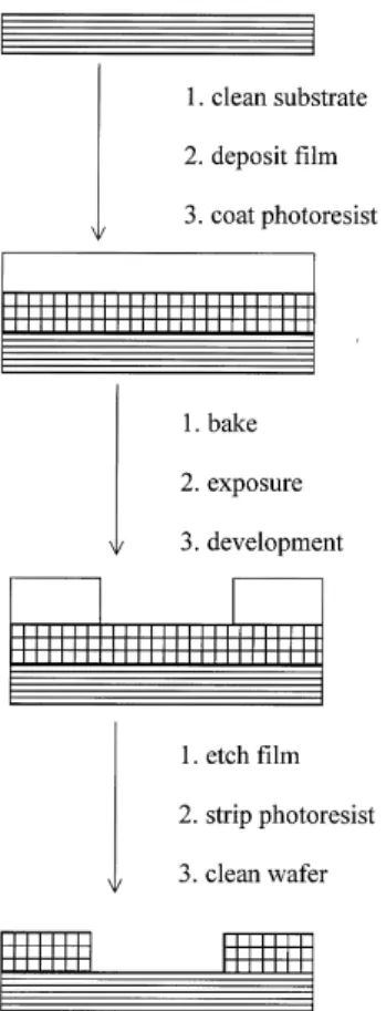
Fig. 1. Part of the process flow for patterning the semiconductor device.
more thorough understanding of the potential of metal diffusion into the silicon substrate during device fabrication is essential to reduce contamination and improve circuit yield [9].
The control of fabrication processes involved in de-vice manufacturing has become increasingly crucial due to the growing complexity of materials and tools [3]. Fig. 1 depicts part of the process flow for pattern-ing the device circuit. Basically, the incompattern-ing wafer needs to be clean prior to deposition of the film (such as silicon oxide, silicon nitride, polysilicon, dielec-tric or metal). The processes of bottom anti-reflective coating (BARC), photoresist (PR) coating, exposure, baking and development should be followed to pattern the deposition film [10]. After lithography, the wafer is etched. The area, protected by the PR, should be tolerant to the etching. After finishing the etching pro-cess, the PR is removed and the pattern is revealed. These processes are generally to be thought of as a
dirty procedure because many organic and inorganic contaminants can be transferred to the wafer surface during etching, especially in the energetic plasma etch-ing process. Therefore, the cleanetch-ing process should succeed in ensuring reliability [3].
In Fig. 1, the wet chemical processes (e.g., cleaning and lithography) play a very important role because they are applied repeatedly to the wafer surface dur-ing device manufacturdur-ing. Contamination may come from the process materials, therefore material purity and cleaning efficiency are of extreme importance. In semiconductor fabrication, the well known RCA cleaning method [11], universally applied in wafer processing for removing the contaminant, was origi-nally developed based on the radioactive tracer method by Kern and Puotinen in 1970. The effectiveness of the RCA cleaning method was established by delib-erately contaminating the wafer surface with radioac-tive nuclides 64Cu and 198Au. Gamma radioactivity was recorded after and before RCA cleaning to mon-itor the cleaning efficiency. Wang et al. first [9] stud-ied the diffusion of Mn and Zn out of lithographic materials into the underlying substrates, and also in-vestigated the cleaning efficiency by using a radioac-tive tracer technique. They report that Mn and Zn in deep ultra-violet (DUV) PR may migrate into the sub-strates under various baking conditions. Fortunately, the presently used cleaning process is very effective for removing the Mn and Zn contamination. However, the cleaning efficiency for other metals, before and after lithography, needs further verification.
Today, the advanced semiconductor device man-ufacturers use graphite furnace atomic absorption spectrometry (GFAAS) to determine ultratrace el-ements in lithographic materials for assuring their quality. These materials include DUV PR (expo-sure wavelength= 248 nm) and i-LINE PR (exposure wavelength= 365 nm). In this method, the sample is digested in an acid mixture in a beaker on a hot-plate [12]. However, throughput and contamination are im-portant issues with such a method. For this reason, it is inevitable that new analytical methods must be developed to meet the requirement of the industry. Plasma-based techniques, such as inductively cou-pled plasma mass spectrometry (ICP-MS) and induc-tively coupled plasma atomic emission spectrometry (ICP-AES), possess the advantage of a simultaneous multi-element capability. However, they require a
rapid, efficient and reliable sample preparation tech-nology to ensure their efficiency and capability. This is because the plasma-based instruments readily suf-fer from matrix induced spectral overlap problems and matrix induced signal intensity changes as a consequence of incomplete sample dissolution [13].
Numerous methods have been used for the destruc-tion of organic samples [14–16]. The open-focused microwave digestion method, in comparison with the closed-vessel microwave method, shows the specific advantages of applicability to large samples (up to 10 g), operating in the ambient atmosphere, no accu-mulating pressure problem, and a relatively small ir-radiation zone. The drawback of the digestion method is the probability of contamination from ambient air, cross contamination between samples, and loss of an-alytes. To solve these problems, the use of a quartz chamber and reflux condenser can minimize the risk of contamination and loss of analytes.
In this work, a radioactive tracer technique was pro-posed to evaluate the cleaning efficiency for Na, Fe and Cs impurities by using currently used cleaning methods. The effects of the dipping temperatures and the types of substrates were tested. In addition, possi-ble mechanisms involved in the metals’ cleaning were discussed. Furthermore, the total dry residual solid method was proposed for evaluating the digestion effi-ciency of the lithographic samples (DUV BARC, DUV PR and i-LINE PR). A suitable digestion recipe was found, and was subsequently employed for matrix dis-solution. The digestion solution after acid evaporation was analyzed by ICP-MS.
2. Experimental
2.1. Materials
Silicon (1 0 0) P-type wafers of 15 cm diameter were deposited with various films (polysilicon, silicon dioxide, silicon nitride), and non-deposited, bare sili-con was used as a sili-control. The wafers were cut into pieces, 2 cm by 2 cm, to serve as test samples. These test samples were subjected to radioactive tracer con-tamination onto the surface to study the cleaning effi-ciency. Carrier-free radioactive tracers from DAMRI (France) were used in this study. The composition
of tracers was 10g g−1 22NaCl (0.873 MBq g−1), 24g g−1 59FeCl3 (0.93 MBq g−1) and 10g g−1 137CsCl (0.747 MBq g−1) in 0.1 M HCl.
Various popular wet cleaning recipes, including SC1, H2O, SC2, DHF, SPM and BOE, were stud-ied in this work. The chemical composition of SC1 solution was conc. ammonia, conc. hydrogen perox-ide and water with a volume ratio of 1 : 1 : 5. The chemical composition of SC2 solution was conc. hy-drochloric acid, conc. hydrogen peroxide and water with a volume ratio of 1 : 1 : 6. The chemical compo-sition of DHF solution was conc. hydrofluoric acid and water with a volume ratio of 1 : 50. The chemical composition of SPM solution was conc. sulfuric acid and conc. hydrogen peroxide with a volume ratio of 4 : 1. The chemical composition for BOE solution was conc. hydrofluoric acid and conc. ammonium fluoride solution with a volume ratio of 1 : 6.
The lithographic materials used in this work were DUV BARC (AZ KrF-12, Clariant, Japan), DUV PR (SEPR-401H, Shin-Etsu Chemical, Japan), and i-LINE PR (IX-850G, Japan Synthesis Rubber, Japan). All reagents used were of analytical or higher grade from Merck (Darmstadt, Germany). High-purity wa-ter, purified by demineralization, two-stage quartz distillation, and sub-boiling distillation, was used throughout. Nitric acid (Merck, Tracepure grade, further treated by in-house sub-boiling), sulfuric acid (Fisher Scientific, Pittsburgh, PA; Tracemetal grade), hydrogen peroxide and hydrochloric acid (both Merck) were used for digestion of the sam-ples. Standard solutions of the analytes were freshly prepared by diluting the concentrated (1000 mg l−1) stock solutions (Merck) with 1% nitric acid.
2.2. Film growing process
To prepare different underlying surfaces for this study, films of polysilicon, silicon oxide, and silicon nitride were deposited onto various starting silicon wafers by low-pressure chemical vapor deposition (LPCVD) in a quartz reactor. The polysilicon film was deposited with silane gas (SiH4) at 60 cm3min−1 and 620◦C. The silicon oxide layer was grown by wet oxidation with a gas mixture of hydrogen (8000 cm3min−1) and oxygen (4999 cm3min−1) at 978◦C. The silicon nitride film was deposited with a
mixture of ammonia (130 cm3min−1) and dichlorosi-lane (SiH2Cl2, 30 cm3min−1) at 780◦C. After de-position, the film thickness is characterized with a Nanospec monitor (Nanometrics, CA). The respective thicknesses of these films are 760, 1150 and 500 nm for polysilicon, silicon oxide and silicon nitride.
2.3. Radioactive tracer experimental procedure To study the effectiveness of various wet clean-ing recipes, 0.2 ml of diluted radioactive tracer (in 0.005 M HCl) solution was added onto the sur-faces of test samples. The samples were dried on a hot-plate at 50◦C. After solvent evaporation, the test samples were counted with the high resolution gamma-ray spectrometer. The counting system fea-tures an HPGe detector coupled with a multi-channel analyzer (CANBERRA AccuSpec, IL) and the usual electronics. The energy resolution of the system was 2.4 KeV at 1332 KeV. The intensities of the gamma rays for22Na (t1/2= 2.602y),59Fe (t1/2= 45.1d) and 137Cs (t
1/2= 30.15y) were monitored at the peak en-ergies of 1274.5, 1099.3 and 661.7 KeV, respectively. The radioactivity of the test samples was recorded by the gamma-ray counting system mentioned above. Subsequently, the test samples were immersed in the respective cleaning solutions, i.e., SC1, H2O, SC2, DHF, SPM, and BOE, at various temperatures for 5 min, to dissolve or desorb the metals. Samples were taken out, immersed in room temperature water to rinse off the residual chemical, and then dried on a hot-plate. The radioactivity emitted from the radioac-tive tracers was again measured. The effecradioac-tiveness of various wet cleaning recipes could thus be assessed based on the ratios of the radioactivities counted after and before wet cleaning.
2.4. Microwave decomposition and sample analysis The open-focused microwave devices of Micro-digest 3.6 (Prolabo, Paris) were composed of two PS-34 pumps, six microwave chambers, six tempera-ture sensors, a fume-scrubbing unit and the controlling console. This system can automatically deliver the dissolution reagents (up to four reagents) without in-termixing. The reagent volume can be introduced from 0 to 99.5 ml in 0.5 ml increments. As this digestion
system was operated at atmospheric pressure, the dissolution process was independently controlled at a given temperature setting by infrared-red monitoring from 100 to 400◦C in each digestion chamber. The microwave energy (at 2450 MHz) is transferred to the solution contained in the quartz digestion vessel. The maximum power achieved for each chamber was 250 W, and can be adjustable in 1% increments from 10 to 100%, or at no power. The dissolution chamber and the reflux condenser were made of high purity quartz.
A lithographic sample (3 ml) was digested in the open-focused microwave system. Table 1 lists the different recipes of various digestion mixtures which were tested to find the best dissolution con-ditions. Upon completion of microwave digestion, the sample was cooled before transferring to another PTFE beaker. The sample solution was heated on
Table 1
Various digestion recipes used for dissolution of lithographic materialsa
Reagent Temperature Power volume limit (◦C) Recipe 1 Step 1 10 ml HNO3 130 30% (75 W) 3 ml H2O2 Step 2 5 ml HNO3 160 50% (125 W) 5 ml H2O2 Recipe 2 Step 1 5 ml HNO3 130 30% (75 W) 5 ml H2SO4 3 ml H2O2 Step 2 5 ml HNO3 160 50% (125 W) 5 ml H2O2 Recipe 3 Step 1 9 ml HNO3 130 30% (75 W) 3 ml HCl 3 ml H2O2 Step 2 5 ml HNO3 160 50% (125 W) 5 ml H2O2 Recipe 4 Step 1 3 ml HNO3 130 30% (75 W) 9 ml HCl 3 ml H2O2 Step 2 5 ml HNO3 160 50% (125 W) 5 ml H2O2
a quartz hot-plate in a clean container (class 100) to evaporate to incipient dryness, and subsequently adding 5 ml of nitric acid (1%). The solution was used for the determination of the metals by ICP-MS (Perkin–Elmer Sciex Elan 5000, Norwalk, CT) and ICP-AES (Perkin–Elmer, Optima 3000). To evaluate the completeness of the various digestion recipes, the solution after digestion was evaporated to dryness. The digestion efficiency was obtained from weighing the ratio of the total dry residual solid, after and before sample digestion and complete reagent evaporation.
3. Results and discussion
3.1. Behaviors of metallic impurities
As reported previously [9], metal impurities would migrate from the BARC and PR into the underlying substrates during the lithographic process. To achieve the best cleaning efficiency for Na, Fe, Zn and Cs, an understanding of the behavior of the surface metals and the reaction pathways is necessary.
It has been reported [17–19] that the electrochemi-cal segregation of metal ions at the interface between cleaning solutions and silicon substrates includes the following three possible mechanisms. The first is re-lated to electronegativity. In general, the differences of electronegativity between the atoms provide an in-dicator of the polarity and the ionic character for the chemical bond. The respective electronegativities [20] are 1.9, 0.93, 1.83, 1.65 and 0.79 for Si, Na, Fe, Zn and Cs. Na, Fe, Zn and Cs have a lower electronegativity than silicon. Due to the fact the metal contaminants (in the ionic form) can not attract electrons from the silicon substrate, electronegativity is ruled out as the segregation mechanism for the metals investigated in this work.
The second mechanism is related to the differences in the enthalpy of oxide formation for the metals and silicon. The mechanism is always to be considered be-cause the cleaning processes of SC1 and SC2 have ox-idation characteristics. The precipitation mechanism is that, during the formation of an oxide on the sili-con surface, metal ions are included as metal oxides. Table 2 summarizes the standard molar enthalpies for the formation of metal fluoride and oxide compounds
Table 2
Standard molar enthalpy of oxide formation at 25◦C in kJ mol−1
Formula 1H NaF −576.6 Na2SiO3 −1554.9 NaOH −425.6 FeF2 −764.4 Fe2O3 −824.2 Fe3O4 −1118.4 Fe2SiO4 −1479.9 ZnF2 −764.4 ZnO −350.5 Zn2SiO4 −1636.7 Zn(OH)2 −641.9 CsF −553.5 Cs2O −345.8 CsOH −417.2 SiO2 −910.7
[20]. A negative enthalpy indicates that oxide forma-tion is a heat releasing process. This observaforma-tion indi-cates that sodium metasilicate, iron(II, III) oxide, iron orthosilicate and zinc orthosilicate are possible struc-tures because of their lower enthalpies than silicon dioxide.
The third mechanism considers the effect of adsorp-tion of the metal ions. This effect is not only depen-dent on the concentration of the metals but also on the electrochemical potential and solution pH. The latter two mechanisms might be responsible as plausible sur-face reactions for Na, Fe, Zn and Cs in the cleaning solutions.
3.2. Evaluation of cleaning efficiency
Six wet cleaning processes, i.e., SC1, H2O, SC2, DHF, SPM, and BOE, are commonly applied in wafer fabrication. Generally, the wet cleaning processes are used to overcome the contamination problem after pat-tern definition. Mixtures of HF and NH4F, known as BOE, are used to etching silicon oxide film and can provide a constant etching rate. Removal or clean-ing of heavy organic material, such as PR and its by-products, can be accomplished with SPM. How-ever, the extents of residual metals after BOE and SPM cleanings should still be carefully evaluated. It is beneficial for the understanding of the residual metal
levels after the standard cleaning process. The cleaning sequence DHF–H2O–SC1–H2O–SC2–H2O, modified from the conventional RCA clean, is well accepted be-cause it shows better cleaning performance on light or-ganic, particulate, and metal species [21]. In this work, various wet processes were tested against its removal efficiency for metal impurities by a radioactive tracer technique. Among the prominent factors affecting the impurity removal efficiency, the substrate types and the cleaning temperatures were studied.
Tables 3–5 list the (percentage) remaining ratios of radioactive tracers for Na, Fe, Zn and Cs after 5 min of treatment in various cleaning recipes at temperatures of 25, 47 and 82◦C. It can be seen that Na and Cs im-purities are not found for any substrates and temper-atures after SC1 cleaning. This observation indicates that alkali metal ions can effectively be removed by SC1 cleaning. However, Fe shows more significant re-tention (>45%) than Zn (<5%), regardless of substrate type and solution temperature. What are the reasons for these different behaviors? According to the behav-iors of metallic impurities mentioned in Section 3.1, the effects of the enthalpy of oxide formation and ad-sorption are the two major reasons. This finding could be explained from Table 2 that, during SC1 cleaning, iron(II, III) oxide and iron orthosilicate were included
Table 3
Residual ratios of radioactive tracers after 5 min of dipping in various cleaning recipes at 25◦C
Substrate Element SC1 (%) H2O (%) SPM (%) BOE (%)
Bare Si Na 0 0 0 0 Fe 95.5 84.7 1.6 0.3 Zna 4.3 10.3 0 0 Cs 0 1.6 0 0 Poly Si Na 0 0 0 0 Fe 92.1 72.0 1.1 0.7 Zna 0.3 0 0 0 Cs 0 0.6 0 0 Silicon oxide Na 0 0 0 0 Fe 86.6 87.9 0 0 Zna 2.7 0 0 5.0 Cs 0 0 0 0 Silicon nitride Na 0 0 1.4 0 Fe 93.9 93.1 0 0.8 Zna 2.1 0 1.8 0.9 Cs 0 0 1.4 0 a[9]. Table 4
Residual ratios of radioactive tracers after 5 min of dipping in various cleaning recipes at 47◦C
Substrate Element SC1 (%) H2O (%) SPM (%) BOE (%)
Bare Si Na 0 0 0 0 Fe 75.2 64.1 0.5 0.2 Zna 0.5 20 0 0.9 Cs 0 0.3 0 0 Poly Si Na 0 0 0 0 Fe 84.7 71.5 0.7 0.2 Zna 0 17.4 0 0.8 Cs 0 1.3 0 0 Silicon oxide Na 0 0 0 0 Fe 73.8 60 0 0 Zna 0 0 0 0 Cs 0 0 0 0 Silicon nitride Na 0 0 0 0 Fe 76.4 88.8 0 0.2 Zna 0 0 0 0 Cs 0 0 0 0
a[9]. Ratios were all 0% for SC2 and DHF.
in the grown silicon oxide, while zinc oxide can not exist on the surface due to the unfavorable enthalpy.
Comparing Table 3 (25◦C) with Table 4 (47◦C), the residual metallic impurities after SC1 treatment generally decrease with increasing with temperature,
Table 5
Residual ratios of radioactive tracers after 5 min of dipping in various cleaning recipes at 82◦C
Substrate Element SC1 (%) H2O (%)
Bare Si Na 0 0 Fe 81.0 65.4 Zna 1.9 0 Cs 0 0 Poly Si Na 0 0 Fe 73.8 83.9 Zna 0 0 Cs 0 0 Silicon oxide Na 0 0 Fe 69.9 45.0 Zna 0 0 Cs 0 0 Silicon nitride Na 0 0 Fe 48.1 36.7 Zna 0 0 Cs 0 0
suggesting that the diffusion of metals between sub-strates and SC1 solution is becoming significant on elevating the temperature. However, from Table 5, the cleaning efficiency at 82◦C is not temperature depen-dent. This tendency could be explained on the basis of the bath life of the cleaning solution as a conse-quence of the change of chemical composition. The temperature strongly affects the lifetime (i.e., bath life) of SC1 solution, especially at higher temperatures. It has been reported that hydrogen peroxide is thermally unstable and ammonia is easily evaporated at higher temperatures [22]. For SC1 reactions, hydrogen per-oxide serves as an oxidant, while ammonia serves to etch away the grown silicon oxide. The etching rates increase with temperature by using SC1 solution. But taking the bath life into consideration, the etching rates could be lowered with increasing temperature.
Water is generally used to rinse off chemicals from the previous cleaning step in wet wafer processes. It is found that the remaining ratios of Na, Zn and Cs become 0 for all underlying substrates at 82◦C. This observation indicates that hot water immersion is very effective for dissolving Na, Zn and Cs from the wafer surface. Also, this finding suggests that the diffusion lengths of these metals are very shallow, and the wafer can easily be cleaned by hot water. However, it should be cautioned that this observation may be true only for Na, Zn and Cs; Fe is still present after hot water dipping (at 82◦C). This may be attributed to either strong adsorption, or the formation of the oxide in hot water dipping.
SC2 solution is found to be satisfactory as a clean-ing agent for removclean-ing Na, Fe, Zn and Cs impurities. Our results clearly show that Na, Fe, Zn and Cs impu-rities can be fully removed at higher temperatures (47 and 82◦C) from any substrate. This occurs because its strong acid (H+) composition effectively replaces the metal ions (i.e., Na+, Fe3+, Zn2+, Cs+) on the wafer surface. Similar behavior is also apparent for cleaning with DHF solution. This result is apparently consistent with that of Anttila et al., who predicted that the con-taminant Zn should be removed in DHF [23], despite the fact that thousands of particles may be added to the wafer surface. The SPM solution also has a strong acid composition, therefore the results are similar to those for SC2 and DHF. No retention effects can be seen at a cleaning temperature of 82◦C, regardless of the sub-strate type. The cleaning efficiency of BOE solution
is only significant at 82◦C for these metals. At room temperature and 42◦C, a proportion of the radioactive metals is counted on the wafer. From these results, we have demonstrated that the metal impurities are ini-tially trapped in the grown native oxide, while BOE dipping at the higher temperature can etch away the whole grown native oxide and remove the tracers.
3.3. Evaluation of digestion efficiency
The previous paper mentions that metal impurities might migrate from lithographic materials into the un-derlying substrate [9]. To prevent the contamination problem, the most effective method is to control the impurity levels in the original BARC and PR. How-ever, it is not easy to determine trace metals in such samples. If using direct instrumental determination, the complex and viscous character of such materials can severely clog the sample loop or the interface to the measuring instrument, thus affecting the analytical reliability. For routine quality control, it is necessary to develop analytical methods which take less time, provide a quick response and a reasonable put for the processes. Taking reliability and through-put into consideration, it is necessary to develop the appropriate pretreatment method for trace metals de-termination. Destruction of the organic matrix with an open-focused microwave system has been used for trace and ultratrace analysis [15,16]. However, to what extent the matrix is destroyed by specific decompo-sition conditions has so far seldom been evaluated quantitatively. Conventionally, when clear and color-less solutions are obtained, or when total recovery of some elements is obtained, it is assumed that oxi-dation of the organic matter has been completed for all practical purposes. However, such assumptions are not necessarily reliable in all cases. More conclusive and direct information as to the amount of resultant residual material is beneficial for choosing the best digestion recipe.
In this study, a gravimetric method was tested for its applicability to evaluate the completeness of sam-ple matrix destruction with various digestion recipes. Table 6 lists the digestion recipe and the digestion ef-ficiency for DUV BARC, DUV PR and i-LINE PR. Prior to the sample analysis, the sample sizes were optimized to achieve the best detection limits (DLs)
Table 6
Effects of digestion efficiency on lithographic materials after open-focused microwave digestion for various recipesa
Sample DUV BARC (%) DUV PR (%) i-LINE PR (%)
Recipe 1 99.8 99.6 96.3 Recipe 1b 96.5 97.2 73.0 Recipe 2 97.9 95.9 95.6 Recipe 3 99.8 96.7 87.7 Recipe 4 97.0 78.7 80.1 aSample volume is 3 ml.
bDigestion only with the first step of Recipe 1.
and fit the scale of the digestion vessel. If a 5 ml sam-ple is used, the abrupt effervescence produced in the first minutes led to the ascent of the digestion solution through the vessel, causing spillover. Such an unsuit-able sample volume should influence the method reli-ability. It can be noted that too large a sample volume increases the reaction (digestion) rate, and produces more effervescence. After testing different amounts of lithographic samples, the upper limit of the sample size is 3 ml. To minimize the dissolution time, the mi-crowave power of the first step was elevated to 50%. However, the same problem arose, the digestion so-lution immediately bubbling out of the vessel, espe-cially for BARC. The working power for the first step should be limited to 30% to assure digestion reliabil-ity. Likewise, the upper temperature limit, the power and the time for the first step of digestion are found to be 130◦C, 30% and 30 min, respectively, while 160◦C, 50% and 30 min are recommended for the second step. The recipes in Table 6 are all effective for DUV BARC digestion, which indicates that the various recipes can easily destroy the matrix with the pro-posed open-focused microwave digestion program. For the DUV PR sample, Recipe 4 is less effective. The further question is how Recipe 3 can better dis-solve the DUV PR sample than Recipe 4 by only changing the aqua regia for ‘reverse’ aqua regia in the first step. This observation shows that nitric acid is more beneficial for the digestion of lithographic sam-ples than hydrochloric acid. A large nitric acid volume (9 ml) enhances the oxidizing ability and facilitates the digestion. This observation also confirms the di-gestion efficiency of Recipe 2, which uses only 5 ml of nitric acid. The presence of 5 ml of sulfuric acid in addition to the 5 ml of nitric acid also exerts powerful oxidation at temperatures above 100◦C. Similar to
Recipes 1 and 3, Recipe 2 can also maintain better digestion efficiency.
For the i-LINE PR, Table 6 indicates that only the Recipes 1 and 2 can achieve better digestion efficiency than the other recipes. The use of only the first step of Recipe 1 is not satisfactory to destroy the matrix. How-ever, the following with the second step with 5 ml of nitric acid and hydrogen peroxide can achieve and en-sure higher digestion efficiency (from 73.0 to 96.3%). Although Recipes 1 and 2 are found to be appropriate for the digestion of lithographic samples, there are two drawbacks when using sulfuric acid for digestion. The first is the high boiling point of sulfuric acid, which requires a long time for reagent evaporation after di-gestion and prior to instrumental analysis. The second is that the incomplete evaporation of the sulfuric acid can induce troublesome mass spectroscopic interfer-ence in the ICP-MS determination. From these view-points, Recipe 1 has been chosen as the best means of decomposing lithographic samples.
3.4. Analysis of lithographic materials
The analytical performance of the open-focused microwave digestion and instrumental determination method were evaluated in terms of detection limit, spike recovery and accuracy. The detection limits of this method are defined as the analyte concentrations that give signal intensities three times the standard deviation of the procedure blank (n= 6). It was esti-mated that the detection limits were in the ng ml−1 and sub-ng ml−1 levels for ICP-MS analysis, and ng ml−1 level for ICP-AES analysis. As shown in Table 7, Na and Al have poor detection limits for both ICP-MS and ICP-AES analysis. This observation can be attributed to the digestion process being operated in an open environment, leading to contamination problems for Na and Al. Except for Al, Ca and Fe, the detection limits for ICP-MS are better than those for ICP-AES. In ICP-MS detection, the consideration of mass spectroscopic interferences is necessary. The background of27Al is elevated by the intense signal at the neighboring peak of m/z= 28 (from N2+ and Si+). 44Ca is generally affected by the polyatomic effect at m/z= 44 from 12C16O2+, and 57Fe from 40Ar16O1H+. For this reason, the detection limits of Al, Ca and Fe are degraded.
Table 7
Detection limits (DLs) for elements in lithographic materials di-gested by an open-focused microwave method, followed with ICP-MS or ICP-AES analysisa
Element ICP-MS ICP-AES
Mass DL (ng ml−1) Wavelength (nm) DL (ng ml−1) Na 23 84 589.6 126 Al 27 20 396.2 15.9 Ca 44 45 396.8 4.5 Cr 52 0.74 267.7 1.2 Fe 57 10.2 259.9 3.9 Ni 60 0.39 231.6 2.4 Cu 65 0.39 324.8 2.4 Zn 66 1.28 213.9 4.8 Au 197 0.57 242.8 3.6 Pb 208 0.22 220.4 4.1 Sn 118 4.04 235.5 14.2 Pt 195 0.28 214.4 5.7 Cs 133 0.1 – –
aThe detection limits are based on three times the standard deviation of the procedure blank (n= 6).
Recovery tests were performed by spiking equivalent amounts of 5 ng ml−1 metals into the open-focused digestion reactor, followed by the use of digestion recipe (Recipe 1, see Table 1) and ICP-MS determination. The results of the spike recovery tests for these metals are shown in Table 8. As can be seen, the spike recoveries for all the analytes except Ca were in the ranges 82–119, 88–121 and 82–112% for DUV BARC, DUV PR and i-LINE PR, respec-tively. The recovery of Ca was not acceptable due to
Table 8
Spike recoveries (%) for lithographic samples digested by open-focused microwave digestion, followed by ICP-MS analysis
Element DUV BARC DUV PR i-LINE PR
Na 102 118 109 Al 119 121 112 Ca 125 146 131 Cr 110 97 82 Fe 99 92 95 Ni 82 100 109 Cu 87 101 100 Zn 100 103 110 Au 99 88 112 Pb 113 92 98 Sn 91 108 101 Pt 90 97 102 Cs 104 100 96 Table 9
Analytical results for lithographic samples digested by open-focused microwave, followed by ICP-MS analysis Element DUV BARC DUV PR i-LINE PR
ng ml−1 RSD (%) ng ml−1RSD (%) ng ml−1 RSD (%) Na 155 9.0 343 2.9 246 1.6 Naa 146 11.6 387 9.8 – – Al 172 35.5 3.63 9.9 49.1 0.6 Ala 178 35.4 ND – – – Ca 292 5.8 192 31.3 207 15.9 Cr 1.90 17.9 8.7 12.6 8.62 1.39 Fe NDb – ND – ND – Ni 0.64 10.9 1.07 25.2 1.70 21.8 Cu 1.65 25.5 3.27 6.7 12.9 2.3 Zn 4.50 34.7 2.20 6.8 6.20 1.9 Au 5.38 12.3 13.2 24.2 1.45 12.5 Pb ND – ND – 1.14 4.4 Sn ND – 6.14 22.1 ND – Pt ND – ND – ND – Cs ND – ND – ND –
aAnalysis by ICP-AES; RSD: relative standard deviation (n= 3).
bND: not detected.
the polyatomic interference from CO2+ in ICP-MS detection. The results of spike recoveries indicate the feasibility by applying the open-focused microwave digestion method and ICP-MS multi-elements deter-mination method for lithographic samples.
The proposed method has already been applied to the determination of metals in semiconductor litho-graphic samples. Table 9 shows the results. The relative standard deviations (RSDs) for DUV BARC, DUV PR and i-LINE PR are within 35.5, 31.3 and 21.8%, revealing that the results all have fairly good precision. Despite no commercial certified refer-ence samples being available for these samples, the literature reports [24], obtained from closed-vessel microwave digestion and ICP-MS analysis, are all in good agreement with this study. In addition, the results for Na and Al by ICP-AES determina-tion also demonstrate the accuracy of the proposed method.
The sample throughput of this method is up to 3.5 h−1for analysis of 13 elements. The conventional method using GFAAS, as proposed in the litera-ture [12], is estimated to accommodate only 0.4 h−1 for 13 elements. Therefore, the proposed method is very suitable for metals determination in lithographic
samples. The analytical throughput of the present method is eight times greater than the conventional GFAAS method.
Acknowledgements
The authors wish to thank the National Science Council, Taiwan, for financially supporting this re-search through contract #NSC88-3011-B-007-010-NU.
References
[1] S.M. Sze, VLSI Technology, 2nd Edition, McGraw-Hill, New York, 1988, Chapter 14.
[2] A.V. Ferris-Prabhu, Introduction to Semiconductor Device Yield Modeling, ARTECH HOUSE, MA, 1992, Chapter 1. [3] C.Y. Chang, S.M. Sze, ULSI Technology, McGraw-Hill, New
York, 1996.
[4] P.J. Ward, J. Electrochem. Soc. 129 (1982) 2573.
[5] M. Miyazaki, M. Sano, S. Sumita, N. Fujino, Jpn. J. Appl. Phys. 30 (1991) L295.
[6] A.L.P. Rotondaro, T.Q. Hurd, A. Kaniava, J. Vanhellemont, E. Simoen, M.M. Heyns, C. Claeys, J. Electrochem. Soc. 143 (1996) 3014.
[7] E.R. Weber, Appl. Phys. A30 (1983) 1. [8] J.-P. Joly, Microelectro. Eng. 40 (1998) 285.
[9] M.-Y. Wang, F.-H. Ko, T.-K. Wang, C.-C. Yang, T.-Y. Huang, J. Electrochem. Soc. 146 (1999) 3455.
[10] S. Nonogaki, T. Ueno, T. Ito, Microlithography Fundamentals in Semiconductor Devices and Fabrication Technology, Marcel Dekker, New York, 1998, Chapter 1.
[11] W. Kern, D.A. Puotinen, RCA Rev. 31 (1970) 187. [12] M. Takenaka, S. Kozuka, Y. Hashimoto, Bunseki Kagaku 42
(1993) T71.
[13] H.M. Kingston, Atom. Spectrosc. 19 (1998) 27.
[14] F.-H. Ko, M.-H. Yang, J. Anal. Atom. Spectrom. 11 (1996) 413.
[15] M. Takenaka, S. Kozuka, M. Hayashi, H. Endo, Analyst 122 (1997) 129.
[16] C.-C. Huang, M.-H. Yang, T.-S. Shih, Anal. Chem. 69 (1997) 3930.
[17] T. Ohmi, T. Imaoka, I. Sugiyama, T. Kezuka, J. Electrochem. Soc. 139 (1992) 3317.
[18] M. Sano, in: Proceedings of the 10th Workshop on ULSI Ultra Clean Technology, Tokyo, Japan, Ultra Clean Society, 1991, p. 55.
[19] L.M. Loewenstein, F. Charpin, P.W. Mertens, J. Electrochem. Soc. 146 (1999) 719.
[20] D.R. Lide, CRC Handbook of Chemistry and Physics, 79th Edition, CRC Press, Boca Raton, FL, 1998.
[21] H. Morinaga, T. Ohmi, Ultra Clean Technol. 8-3 (1996) 144. [22] W. Kern, Semicond. Int. 7 (1984) 94.
[23] O.J. Anttila, M.V. Tilli, M. Schaekers, L.L. Claeys, J. Electrochem. Soc. 139 (1992) 1180.
[24] F.-H. Ko, L.-T. Hsiao, C.-T. Chou, M.-Y. Wang, T.-K. Wang, Y.-C. Sun, B.-J. Cheng, S. Yeng, B.-T. Dai, Proc. SPIE 3677 (1999) 907.