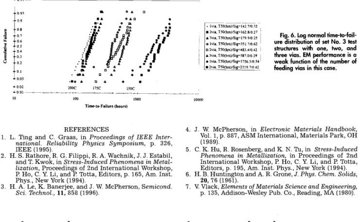
J Electrochem. Soc., Vol. 144, No. 7, July 1997 The Electrochemical Society, Inc. 2525 [i5o1hcs)1SigI42 7/0 32 • 2via, TSO(s)JSigt62.0iQ,27 £ 3va, T50(h,s)ISi0=179 9/025 o Ivia, T50(h,s)/Sir351 710.62 0 2via, T50(hos)ISig=4S3.410.42 Sv,a, T50(hrs)/Sig—5a7.O/0 29 • ivia, T50(h,s)lSgl756.3/0,54
•
2v,a. T90(hrs)/Sjg.23I9 7/042Fig. 6. Log normal time-to-fail-ure distribution of set No. 3 test sfructures with one, Iwo, and three vias. EM performance is a weak function of the number of feeding vias in this case.
Tune to-Failure (bour)
REFERENCES
1. L. Ting and C. Graas, in Proceedings of IEEE
Inter-national. Reliability Physics Symposium, p. 326,
IEEE (1995).2. H. S. Rathore, R. G. Filippi, R. A. Wachnik, J. J. Estabil,
and T. Kwok, in Stress-Induced Phenomena in
Metal-lization, Proceedings of 2nd International Workshop,
P. Ho, C. Y. Li, and P. Totta, Editors, p. 165, Am. Inst. Phys., New York (1994).
3. H. A. Le, K. Banerjee, and J. W McPherson, Semicond.
Sci. Technol., 11,858(1996).
4. J. W. McPherson, in Electronic Materials Handbook,
Vol. 1, p. 887, ASM International, Materials Park, OH (1989).
5. C. K. Hu, R. Rosenberg, and K. N. Tu, in Stress-Induced
Phenomena in Metallization, in Proceedings of 2nd
International Workshop, P. Ho, C. Y. Li, and P. Totta,
Editors, p. 195, Am. Inst. Phys., New York (1994). 6. H. B. Huntington and A. R. Grone, J. Phys. Chem. Solids,
20, 76 (1961).
7. V. Vlack, Elements of Materials Science and Engineering, p. 135, Addison-Wesley Pub. Co., Reading, MA (1980).
Plasma Charging Damage and Water-Related Hot-Carrier
Reliability in the Deposition of Plasma-Enhanced
Tetraethylorthosilicate Oxide
Y. M. Lin,° S. M. Jang,b C. H. Yu,b 1. F. Lei,° and J. Y. Chenb"Department
of Electronics Engineering and Institute of Electronics, National Chiao-Tung University, Hsin-Chu, Taiwan
bTaiwan Semiconductor Manufacturing Company, Research and Development, Hsin- Chu, Taiwan
ABSTRACT
This paper presents plasma-enhanced tetraethylorthosilicate oxide process (PETEOS) induced hot-carrier reliability
associated with an intermetallic dielectric formed by depositing oxide films from PETEOS, ozone-TEOS, and spin-on
glass (SOG), where a single or dual-frequency PETEOS film is deposited as an underlayer followed by an ozone-TEOS
deposition for gap filling and a SOG coating for planarization. The impact of PETEOS process conditions such as
low-and high-frequency plasma power low-and PETEOS film thickness on hot-carrier reliability are studied. It is observed that
increasing the low- and! or high-frequency plasma power can improve the film quality and moisture-related hot carrier
immunity, but at the expense of plasma charging damage. This plasma charging damage accumulates gradually and
final-ly saturates as the deposition of oxide from PETEOS proceeds. In general, a thick PETEOS layer is desired for
improv-ing the moisture-related hot carrier immunity. As a result, there is a trade-off between the plasma chargimprov-ing damage and
the related hot carrier immunity. The plasma charging damage is dominant in large devices and the
moisture-related hot-carrier immunity is dominant in small devices.
Introduction
Plasma-enhanced
tetraethylorthosilicate (PETEOS)
based oxide films are extensively used as intermetallic
dielectrics (IMDs) due to their good step coverages as well
as good electrical and mechanical properties.5
Ozone-TEOS oxide has been a promising IMD candidate for
sub-0.5 im processes. However, owing to substrate
depen-dency, moisture absorption, and cracking tendency of
ozone-TEOS oxide, a compressive PETEOS is usually
deposited prior to ozone-TEOS deposition. Recently, it is
reported that moisture resistance of PETEOS films is
improved by increasing the low frequency power but
plas-ma daplas-mage is increased.2
In very large scale integrated (VLSI) fabrication, the gate
oxide is often degraded due to the charge collected at the
gate electrode during plasma processing such as polysilicon reactive ion etching (RIE) etch, plasma resist stripping, and
plasma etching of aluminum.3-5 However, little has been
reported with regard to charging damage from PETEOS
deposition.0 Recently, we reported the improvement of
device reliability in single- and dual-frequency PETEOS
processes.5 In this paper, we investigate the impact of
PETEOS process conditions such as plasma frequency,plas-ma power, and PETEOS oxide film thickness on gate oxide
integrity as well as hot-carrier aging.
Experimental
The PECVD-TEOS and subatmospheric CVD (SACVD)
03-TEOS reactor used in this study is implemented in a
multichamber single-wafer tool which was described in
a, C 0 09904 0
IA 080 0,9 l.A 0•4
0 08
00.4
0 04
:
107 106 1.03 02.,
fr7
0.4 0,34 0
A• U
0 A S U 0,10.03 .10 £.014
0 4
0 A•
S U 40,02 200C 179C 150C 10 100 1000 10000J. Electrochem. Soc., Vol. 144, No. 7, July 1997 C The Electrochemical Society, Inc.
095 & * 0.9 01 /^ Ala D *A 0 os O·3 * DA12 +002 200C 17SC 150C 0201 · 10 100 1000 100 Time-to-Failure (hours) lIvia, T50(hs)/Sig=142,7/0.32 * 2via, T50(hrs)Sig-162.80.27 A 3via, T50(hs)Sig= 179 910.25 O Ivia, T50(hrs)/Sigf351 710.62 O 2via, T50(hrs)/Sig-483.4/0.42 A 3via, T50(hrs)/Sig=587.0 0 29 * 1via, T50(hrs)/Sig 1756.3/0.54 * 2via. T50(hs)/Sig-23197/0 42
Fig. 6. Log normal time-to-fail-ure distribution of set No. 3 test
structures with one, two, and three vias. EM performance is a weak function of the number of feeding vias in this case.
o00
REFERENCES
1. L. Ting and C. Graas, in Proceedings of IEEE
Inter-national. Reliability Physics Symposium, p. 326,
IEEE (1995).
2. H. S. Rathore, R. G. Filippi, R. A. Wachnik, J. J. Estabil, and T. Kwok, in Stress-Induced Phenomena in
Metal-lization, Proceedings of 2nd International Workshop,
P. Ho, C. Y. Li, and P. Totta, Editors, p. 165, Am. Inst. Phys., New York (1994).
3. H. A. Le, K. Banerjee, and J. W. McPherson, Semicond.
Sci. Technol., 11, 858 (1996).
4. J. W. McPherson, in Electronic Materials Handbook, Vol. 1, p. 887, ASM International, Materials Park, OH (1989).
5. C. K. Hu, R. Rosenberg, and K. N. Tu, in Stress-Induced
Phenomena in Metallization, in Proceedings of 2nd
International Workshop, P. Ho, C. Y. Li, and P. Totta, Editors, p. 195, Am. Inst. Phys., New York (1994). 6. H. B. Huntington and A. R. Grone, J. Phys. Chem. Solids,
20, 76 (1961).
7. V. Vlack, Elements of Materials Science and Engineering, p. 135, Addison-Wesley Pub. Co., Reading, MA (1980).
Plasma Charging Damage and Water-Related Hot-Carrier
Reliability in the Deposition of Plasma-Enhanced
Tetraethylorthosilicate Oxide
Y.
M. Lin," S. M. Jang,
bC. H.
Yu,b
T. F. Lei,a and J. Y. Chenb
'Department of Electronics Engineering and Institute of Electronics, National Chiao-Tung University, Hsin-Chu, Taiwan bTaiwan Semiconductor Manufacturing Company, Research and Development, Hsin-Chu, Taiwan
ABSTRACT
This paper presents plasma-enhanced tetraethylorthosilicate oxide process (PETEOS) induced hot-carrier reliability associated with an intermetallic dielectric formed by depositing oxide films from PETEOS, ozone-TEOS, and spin-on glass (SOG), where a single or dual-frequency PETEOS film is deposited as an underlayer followed by an ozone-TEOS deposition for gap filling and a SOG coating for planarization. The impact of PETEOS process conditions such as low-and high-frequency plasma power low-and PETEOS film thickness on hot-carrier reliability are studied. It is observed that increasing the low- and/ or high-frequency plasma power can improve the film quality and moisture-related hot carrier immunity, but at the expense of plasma charging damage. This plasma charging damage accumulates gradually and final-ly saturates as the deposition of oxide from PETEOS proceeds. In general, a thick PETEOS layer is desired for improv-ing the moisture-related hot carrier immunity. As a result, there is a trade-off between the plasma chargimprov-ing damage and the related hot carrier immunity. The plasma charging damage is dominant in large devices and the moisture-related hot-carrier immunity is dominant in small devices.
Introduction
Plasma-enhanced tetraethylorthosilicate (PETEOS) based oxide films are extensively used as intermetallic dielectrics (IMDs) due to their good step coverages as well as good electrical and mechanical properties.1 Ozone-TEOS oxide has been a promising IMD candidate for sub-0.5 tm processes. However, owing to substrate depen-dency, moisture absorption, and cracking tendency of ozone-TEOS oxide, a compressive PETEOS is usually deposited prior to ozone-TEOS deposition. Recently, it is reported that moisture resistance of PETEOS films is improved by increasing the low frequency power but plas-ma daplas-mage is increased.2
In very large scale integrated (VLSI) fabrication, the gate oxide is often degraded due to the charge collected at the
gate electrode during plasma processing such as polysilicon reactive ion etching (RIE) etch, plasma resist stripping, and plasma etching of aluminum.3- However, little has been reported with regard to charging damage from PETEOS deposition." s Recently, we reported the improvement of device reliability in single- and dual-frequency PETEOS processes.5 In this paper, we investigate the impact of PETEOS process conditions such as plasma frequency, plas-ma power, and PETEOS oxide film thickness on gate oxide integrity as well as hot-carrier aging.
Experimental
The PECVD-TEOS and subatmospheric CVD (SACVD) O3-TEOS reactor used in this study is implemented in a
multichamber single-wafer tool which was described in
t
I
d
2526 J. Electrochem. Soc., Vol. 144, No. 7, July 1997 The Electrochemical Society, Inc.
Ref. 19. These PETEOS films are generated by a single
(13.56 MHz), or dual (13.56 MHz and 350 KHz), radio
fre-quency (RF) supply. TEOS and oxygen were used as
reac-tants and the deposition temperature was set at 400°C.
PETEOS oxide film was deposited to 0.1—0.3 tim,
fol-lowed by an ozone-TEOS deposition at 400°C without
plasma enhancement. Spin-on-glass (SOG) was then
applied for planarization. Finally, a plasma-enhanced
silane oxide is deposited to terminate the IMD process.
Gate oxide thickness is 14.6 or 10 nm. A 0.5 p.m
comple-mentary metal oxide semiconductor (CMOS) process was
used for device fabrication. A complete list of
experimen-tal parameters is shown in Table I.
To characterize gate oxide damage from PETEOS oxide
deposition, the lifetime of n- and p-MOSFETs with and/or
without antenna structure were tested by HP4145B. Large
area capacitors were also tested using time dependent
dielectric breakdown (TDDB). TDDB characteristics were
examined by applying a constant current stress. The total
current passing through the oxide is integrated to yield the
charge-to-breakdown value, Q,. All measurements were
performed at room temperature.
Resultsand Discussion
Comparison
of device reliability between single- and
dual-frequency PETEOS oxide film—The advantages of
dual-frequency PECVD for the deposition of IMD films has
been reported.9"° But the role of plasma on device damage
and reliability is not well understood. In this paper, we first
compare the device reliability with a PETEOS oxide film
deposited by single- and dual-frequency PECVD. The key
experimental parameters are described in Table I (rows 1
and 2). The stress of single- and dual-frequency PETEOS
films are all 1 x 10' dyn/cm2. Figure 1 compiles the Weibull
plot of charge to breakdown (Qbd) for single- and
dual-fre-quency PETEOS IMD capacitor structures. The capacitor
area is 0.01 cm2; 30 capacitors were stressed for each of the oxide. The measurement was made using a constant current stress of —6.7 mA/cm2. The lower charge (—0-6 C/cm2)
sec-tions of the curves in Fig. 1 refer to the defect-related
com-ponents and the higher charge sections of the curves
repre-sent the intrinsic breakdown strength of the oxides. The
devices with dual-frequency PETEOS oxide layers have
smaller intrinsic Qbd and more defects than that of
single-frequency PETEOS oxide layers. However, our wet etch rate
test results show the quality of dual frequency PETEOS
oxide films are better than that of single-frequency
PETEOS oxide films. The moisture resistance of PETEOS
oxides are improved by using dual-frequency PECVD.
In order to investigate the charge trapping
characteris-tics, the Fowler-Nordheim tunneling current stress test
was also performed with constant current of —6.7 mA/cm2for 200 s. n-Channel transistors with gate electrodes
0.7 p.m long and 50 p.m wide were measured. As shown in
Fig. 2, initially all devices show very tight V, distributions.
After constant current stress, devices with dual-frequency
PETEOS oxide show more highly scattered Vs than
devices with single-frequency PETEOS oxide. Note that
No. Gate oxide thickness (nm) Underlayer thickness (km) Low-frequency (350 kHz) power High-frequency (13.56 MHz) power 1 14.6 0.2 H 2 14.6 0.2 L L 3 14.6 0.15 M L
4
10 0.1 L 5 10 0.1 M 6 10 0.1 H 7 10 0.2 H 8 10 0.3 HFig. 1. Weibull plot of charge to breakdown for single- and dual-frequency PETEOS IMD oxide film stressed at a current densi-ty of —6.7 mA/cm2.
after
constant current stress, the difference of average
mean V, between single and dual frequency exceeds 1 V.The importance of an IMD in controlling hot-carrier
performance has been reported previously.1' In this work,
we examine the impact of single- and dual-frequency
PETEOS oxide layers on the n-MOSFETs hot carrier
immunity. Figure 3 compiles device lifetime vs. the
sub-strate current per unit gate width for devices with single
or dual frequency PETEOS oxidelayers. n-MOSFETs with
gate electrode 0.5 p.m long and 20 p.m wide were stressed
at selected 17g.and174,
to
give maximum substrate current.
Device lifetime was determined using a criterion of 10%
transconductance (gm) decrease during the stress. The
n-MOSFETs with dual frequency PETEOS oxide layers
have less hot-carrier immunity.
The moisture resistance of PETEOS oxide layers and
their device hot-carrier reliability are inversely affected
by processing. Recently, it was reported that charging
damage results from PETEOS deposition.2'4 In this work,
we study the transconductance (gm) and saturation
cur-rent (Idsat) degradation in antenna attached to n- and
p-MOSFETs stressed at peak substrate current (Isub) and gate
current (Is), respectively. The antenna structure used in
this study is shown in Fig. 4. Figure 5 shows the changes
in transconductance and saturation current with stress
time. Dual-frequency PETEOS leading enhanced gm and
Idsat degradation compared to single-frequency process
shows the enhanced interface trap generation and electron
Charge to Breakdown (C/cm2)
Table I. List of key experimental parameters.
00 80 60 40 20 5)
a
I) U 1-0) 5) UNote: H: high; M: medium; L: low.
—-— Dual-frequency —0-— Single-frequency —.—--Dual-frequency(F-N) —0-— Single-frequency (F.N) Threshold Voltage (V1) 0 1 2 3 4 5 6 7
Fig. 2. Cumulative distribution of threshold voltage before and
after constant current (—6.7 mA/cm2) stress.
8
J. Electrochem. Soc.,
Vol. 144, No. 7, July 1997©
The Electrochemical Society, Inc.Ref. 19. These PETEOS films are generated by a single (13.56 MHz), or dual (13.56 MHz and 350 KHz), radio fre-quency (RF) supply. TEOS and oxygen were used as reac-tants and the deposition temperature was set at 400°C. PETEOS oxide film was deposited to 0.1-0.3 pLm, fol-lowed by an ozone-TEOS deposition at 400°C without plasma enhancement. Spin-on-glass (SOG) was then applied for planarization. Finally, a plasma-enhanced silane oxide is deposited to terminate the IMD process. Gate oxide thickness is 14.6 or 10 nm. A 0.5 m comple-mentary metal oxide semiconductor (CMOS) process was used for device fabrication. A complete list of experimen-tal parameters is shown in Table I.
To characterize gate oxide damage from PETEOS oxide deposition, the lifetime of n- and p-MOSFETs with and/or without antenna structure were tested by HP4145B. Large area capacitors were also tested using time dependent dielectric breakdown (TDDB). TDDB characteristics were examined by applying a constant current stress. The total current passing through the oxide is integrated to yield the charge-to-breakdown value, Qbd. All measurements were performed at room temperature.
Results and Discussion
Comparison of device reliability between single- and dual-frequency PETEOS oxide film.-The advantages of
dual-frequency PECVD for the deposition of IMD films has been reported.9 ' 0But the role of plasma on device damage and reliability is not well understood. In this paper, we first compare the device reliability with a PETEOS oxide film deposited by single- and dual-frequency PECVD. The key experimental parameters are described in Table I (rows 1
and 2). The stress of single- and dual-frequency PETEOS films are all 1 10' dyn/cm2. Figure 1 compiles the Weibull plot of charge to breakdown (Qbd) for single- and
dual-fre-quency PETEOS IMD capacitor structures. The capacitor area is 0.01 cm"; 30 capacitors were stressed for each of the oxide. The measurement was made using a constant current
stress of -6.7 mA/cm2. The lower charge (-0-6 C/cm2 ) sec-tions of the curves in Fig. 1 refer to the defect-related com-ponents and the higher charge sections of the curves repre-sent the intrinsic breakdown strength of the oxides. The devices with dual-frequency PETEOS oxide layers have smaller intrinsic Qbd and more defects than that of single-frequency PETEOS oxide layers. However, our wet etch rate test results show the quality of dual frequency PETEOS oxide films are better than that of single-frequency PETEOS oxide films. The moisture resistance of PETEOS oxides are improved by using dual-frequency PECVD.
In order to investigate the charge trapping characteris-tics, the Fowler-Nordheim tunneling current stress test was also performed with constant current of -6.7 mA/cm2 for 200 s. n-Channel transistors with gate electrodes 0.7 m long and 50 m wide were measured. As shown in Fig. 2, initially all devices show very tight V, distributions. After constant current stress, devices with dual-frequency PETEOS oxide show more highly scattered Vs than devices with single-frequency PETEOS oxide. Note that
Table . List of key experimental parameters.
Gate oxide Underlayer Low-frequency High-frequency
thickness thickness (350 kHz) (13.56 MHz)
No. (nm) (Arm) power power
1 14.6 0.2 H 2 14.6 0.2 L L 3 14.6 0.15 M L 4 10 0.1 L 5 10 0.1 M 6 10 0.1 H 7 10 0.2 H 8 10 0.3 H
Note: H: high; M: medium; L: low.
Charge to Breakdown (C/cm2)
Fig. 1. Weibull plot of charge to breakdown
(Q)
for single- and dual-frequency PETEOS IMD oxide film stressed at a current densi-ty of -6.7 mA/cm2.after constant current stress, the difference of average mean Vtbetween single and dual frequency exceeds 1 V.
The importance of an IMD in controlling hot-carrier performance has been reported previously" In this work, we examine the impact of single- and dual-frequency PETEOS oxide layers on the n-MOSFETs hot carrier immunity. Figure 3 compiles device lifetime vs. the sub-strate current per unit gate width for devices with single or dual frequency PETEOS oxidelayers. n-MOSFETs with gate electrode 0.5 lm long and 20 pim wide were stressed at selected Vg, and V, to give maximum substrate current. Device lifetime was determined using a criterion of 10% transconductance (gm) decrease during the stress. The n-MOSFETs with dual frequency PETEOS oxide layers have less hot-carrier immunity
The moisture resistance of PETEOS oxide layers and their device hot-carrier reliability are inversely affected by processing. Recently, it was reported that charging damage results from PETEOS deposition."4 In this work, we study the transconductance (gin) and saturation cur-rent (Idsat) degradation in antenna attached to n- and p-MOSFETs stressed at peak substrate current (ub) and gate current (Ig), respectively. The antenna structure used in this study is shown in Fig. 4. Figure 5 shows the changes in transconductance and saturation current with stress time. Dual-frequency PETEOS leading enhanced gm and
Idsat degradation compared to single-frequency process
shows the enhanced interface trap generation and electron
100 e) U 0) a,Uc) E > E :J 80 60 40 20 Threshold Voltage (V)
Fig. 2. Cumulative distribution of threshold voltage before and after constant current (-6.7 mA/cm2) stress.
2526
J Electrochem. Soc., Vol. 144, No. 7, July 1997 The Electrochemical Society, Inc. 2527
'sub' W8 ( .tm)
Fig. 3. n-Channel transistor hot-carrier lifetime vs. substrate cur-rent per unite gate width for single- and dual-frequency PETEOS oxide layer. Each data point is an average of several measurements.
trapping
in the dual-frequency process. The addition of
HF power at 350 kHz increases low frequency ion
bom-bardment which reduces hydrogen content and improves
film density, quality, and moisture resistance.'° The
degraded device hot carrier reliability associated with
dual-frequency PETEOS underlayer may be due to the
more pronounced plasma damage.
Low-frequency plasma power effect—In the dual-f
re-quency (350 kHz and 13.56 MHz) PECVD, the
low-fre-quency plasma power provides ion
bombardment/implan-tation to densify the film and render an intrinsic
compressive stress.9 We improve the moisture resistance of an PETE OS oxide layer ,thecharge to breakdown (Qbd)ofgate oxide and n-MOSFETs hot carrier immunity by
increasing the low-frequency power to get the high
com-pressive stress PETEOS oxide film.2 It was reported that
3 X 10' dyn/cm TEOS-N20 oxides contain more Si-H
bonding at 2260 to 2100 cm' then 1 X 10' TEOS-N20
oxide film.2° The presence of Si-H bonding in the high
stress oxide can enhance the moisture resistance.2'
However, increasing the low frequency plasma power
increases the plasma charging damage. Figure 6 shows the
cumulative distribution of p-MOSFETs hot-carrier
life-time defined as a 5% increase in saturation current (Idsat)
with antenna ratio 1051 —
4205.PETEOS underlayers
were deposited by dual frequency PECVD with varied
low-frequency plasma powers set to —1:2 for comparison.
The key experimental parameters are described in Table I
Plasma
1 1 1 1 1 1 1
Fig. 4. The cross section of the test structure with a large charge collecting antenna.
1000 2000 3000 4000 5000
Stress
Time (see)
Fig. 5. (a, top) The degradation of transconductance in
n-MOSFETs for single- and dual-frequency PETEOS oxide layer. (b, bottom) The degradation of saturation current in p-MOSFETs for sin-gle- and dual-frequency PETEOS oxide layer.
(rows
2 and 3). p-MOSFETs with a gate electrode 1.0 sm
long and 20 m wide were stressed at selected Vd,
andVg5to give the maximum gate current. It is reported that
under condition where bulk electron trapping is the
dom-inant hot carrier degradation mechanism (p-MOSFETs
stressed at peak fg) the hot-carrier induced failure times
depend strongly on antenna ratio.'2 As shown in Fig. 6, a
dependence of device lifetime on antenna ratio increases is
Lifetime (sec)
Fig. 6. Cumulative distribution of hot-carrier lifetime of p-MOSFETs without protection diode for single- and dual-frequency PETEOS oxide layer and various antenna areas.
0 a) La a) E
-I
1 0' 0 —e—Dual-frequency —-c-—Single-frequency 7 8 9 10 2011
10
0 1% 0 S 08
S5 0
7.
06 -
AntennaRatio=4205
5 -.
0
• Dual-frequency
4
0 Singlefrequency
-3 L_ I..h .1.1 ___
0 C 0IC
-a
a
—
-a
a
IC
2000 4000 6000 8000 10000Stress
Time (see)
6 S 5 4 4 S 0 5 0
0
0 S AntennaRatio=1051
-•
Dual-frequency
-0Single-frequency
a) 00a
a) 0 a) a) Ca0
IMD PE-TEOS/SOG;PE-Silane) I lst.Metnl BPSG Polycide-Gate Field-Oxide Si-Substrate Gate-Oxide 100 1000J. Electrochem. Soc., Vol. 144, No. 7, July 1997 © The Electrochemical Society, Inc.
1 0s U I) U E I)
2,
04 7 8 9 10 20 4 4 ES \E 64 I b/ W ( m)Fig. 3. n-Channel transistor hot-carrier lifetime vs. substrate cur-rent per unite gate width for single- and dual-frequency PETEOS oxide layer. Each data point is an average of several measurements.
trapping in the dual-frequency process. The addition of RF power at 350 kHz increases low frequency ion bom-bardment which reduces hydrogen content and improves film density, quality, and moisture resistance. 0 The degraded device hot carrier reliability associated with dual-frequency PETEOS underlayer may be due to the more pronounced plasma damage.
Low-frequency plasma power effect.-In the
dual-fre-quency (350 kHz and 13.56 MHz) PECVD, the low-fre-quency plasma power provides ion bombardment/implan-tation to densify the film and render an intrinsic compressive stress.9 We improve the moisture resistance of an PETEOS oxide layer, the charge to breakdown (Qbd) of gate oxide and n-MOSFETs hot carrier immunity by increasing the low-frequency power to get the high com-pressive stress PETEOS oxide film.2 It was reported that 3 x 10⁹ dyn/cm2 TEOS-N20O oxides contain more Si-H bonding at 2260 to 2100 cm-' then 1 x 10⁹ TEOS-N20
oxide film.2 0 The presence of Si-H bonding in the high stress oxide can enhance the moisture resistance."' However, increasing the low frequency plasma power increases the plasma charging damage. Figure 6 shows the cumulative distribution of p-MOSFETs hot-carrier life-time defined as a 5% increase in saturation current (Id,,t) with antenna ratio 1051 - 4205. PETEOS underlayers were deposited by dual frequency PECVD with varied low-frequency plasma powers set to -1:2 for comparison. The key experimental parameters are described in Table I
Plasma
I I I
i
I I I
Fig. 4. The cross section of the test structure with a large charge collecting antenna. '--o )-,,
<3
I I 10 9 8 7 6 5 4 3 6 5 5 4 4 3 0 o 2000 4000 6000 8000 10000Stress Time (sec)
1000 2000 3000 4000 5000
Stress Time (sec)
Fig. 5. (a, top) The degradation of transconductance in
n-MOSFETs for single- and dual-frequency PETEOS oxide layer. (b, bottom) The degradation of saturation current in p-MOSFETs for sin-gle- and dual-frequency PETEOS oxide layer.
(rows 2 and 3). p-MOSFETs with a gate electrode 1.0 jim long and 20 Rm wide were stressed at selected V,, and Vg, to give the maximum gate current. It is reported that under condition where bulk electron trapping is the dom-inant hot carrier degradation mechanism (p-MOSFETs stressed at peak I) the hot-carrier induced failure times depend strongly on antenna ratio.12
As shown in Fig. 6, a dependence of device lifetime on antenna ratio increases is
r, U to CM qa U . 0-a U 100 1 00 Lifetime (sec)
Fig. 6. Cumulative distribution of hot-carrier lifetime of p-MOSFETs without protection diode for single- and dual-frequency PETEOS oxide layer and various antenna areas.
al-r 0 S e --- Dual-frequency -- Single-frequency
I
* 0 0 S 0 0 Antenna at 0 o * Dual-frequency o Single-frequency i I I I · o -0 0 0 o Antenna Ratio=1051 * Dual-frequency o Single-frequency IMD (PE-TEOS/SOG/PE-Silane) Polycide-Gate4 Field-Oxide BPSG GaeOxd Si-Substrate Gate-Oxide2527
I 1 032528 J. Electrochem. Soc., Vol. 144, No. 7, July 1997 The Electrochemical Society, Inc.
indicative of plasma charging damage. In all cases, the
wafer center suffers more damage than the wafer edge,
suggesting nonuniform plasma distribution across the
wafer. However, the lifetime of p-MOSFETs without an
antenna structure connected is all the same.2 Clearly,
PETEOS deposition has induced plasma damage on
devices as manifested by antenna.
Before IMD deposition, the first metal is divided into
many small individual conductors and is similar to the
overetched poly-gate during RIE poly etching. When the
plasma is nonuniform, a spatially nonuniform plasma
potential V exists and the potential of the floating wafer
surface V1 tracks the plasma potential V.'2 The primary
concern with the charging lies in the dc spatial
nonunifor-mity that exists in V which is forced to be dropped across
the wafer oxide. The reason the voltage changes for
differ-ent frequencies is that the capacitive reactance of oxide
goes like 1/f C. For the ac charging, effect peak to peak volt-age swing V across the gate-oxide due to ac charging is13=
[0.6fliJde/(2.2 X 106)f][(1 +
RA)/1
+
4J]
[1]where n,
M, de, and f
areplasma density, electron
tem-perature, electron mass, gate-oxide thickness, and
bias-frequency. RA =AI/A
and Rd =
d1/ddenote the antenna
ratio and thickness ratio, respectively. A1, A1, d1, and d are
field oxide area, gate oxide area, field oxide thickness, and
gate oxide thickness, respectively. An interesting
predic-tion of Eq. 1 is the bias-frequency dependence of ac
anten-na effect. For a given plasma density, the longer the RF
period, the more ions the surface per cycle collects.13
Consequently, the lower the frequency, the higher the gate
oxide degradation from ac charging. Obviously, the
plas-ma charging daplas-mage of dual-frequency PECVD is larger
than that of single-frequency PECVD.
Hot-carrier reliability degradation caused by plasma
charging damage can be simulated as a Fowler-Nordheim
type J .
t stressthat generates interface traps and bulk
electron traps.8 These interface traps can be passivated by
moisture-related components during the IMD deposition.
At the same time, the bulk traps would be emptied but not
removed.12 As-processed devices (before any stress) show
no symptoms of current flow-induced damage. But the
latent defects give rise to more defect-related early
break-down in devices with dual frequency PETEOS oxide
lay-ers as shown in Fig. 1. As shown in Fig. 2 and 3 harmful
effects may be initiated by F-N stressing and hot-carrier
stressing which cause electrons to be trapped at the
dam-aged sites and cause degraded hot-carrier immunity,
respectively.High-frequency plasma power effect.—PECVD films
with improved integrity, i.e., lower porosity and improved
bulk density could be deposited by raising high-frequency
(13.56 MHz) plasma power.14 Increased RF (13.56 MHz)
power density yielded oxides which were structurally
more relaxed and homogeneous. In this work, the impact
of high-frequency plasma power on the device reliability
is reported for the first time. Single-frequency PETEOS
oxide layers were deposited with varied high-frequency
plasma power. The key experimental parameters are
described in Table I (rows 4, 5, and 6), respectively.
Characteristics of charge to breakdown (Q84)
shownin
Fig. 7 indicates Qbd can be improved by increasing
high-frequency plasma power from 325 to 500 W and finally
saturates with 675 W. The Qbd measurements were made
with a Fowler-Nordheim injection current level of
—5 mA/cm2 over a gate oxide capacitor of i0 cm2. To
characterize the PETEOS quality, thermal desorption
spectroscopy (TDS) was used to determine the amount of
H20 in the films. Our TDS data (not shown) shows the H2O
in the films can be lessened by increasing high-frequency
plasma power. Table II lists the normalized n-MOSFETs
hot-carrier lifetime for varied high-frequency plasma
power and PETEOS oxide layer thickness. For every
Charge to
Breakdown (C/cm2)Fig.7. Weibull plot of charge to breakdown (Q) of capacitors
with varied high-frequency power single-frequency PETEOS IMD oxide layer.
process
condition, 20 devices were stressed at selected Vg,
and VdS which give maximum substrate current. Comparedwith devices with high-frequency plasma power of 350
and 500 W, the hot-carrier lifetime can be prolonged by
increasing the high-frequency plasma power. When the
power is raised to 625 W, the hot-carrier lifetimes are
degraded. According to previous discussions and Ref. 14, itis speculated that plasma charging damage exists and
moisture resistance of the films is degraded if
high-fre-quency plasma power is increased over some critical value.Figure 8 compiles the hot-carrier lifetime of p-MOSFETs
with an antenna ratio of about 1810 across the wafer for
different high-frequency plasma power. p-MOSFETs with
gate electrodes 0.5 p.m long and 9.0 p.m wide were stressed
at V4, -
—5.9V and Vg, - —1.4V giving the peak gate
cur-rent. For the devices sited at wafer edge, the trend of
p-MOSFET is opposite to that of n-MOSFETs of Table II,
which is consistent with Ref. 2. This phenomenon may
suggest the moisture resistance of 675 W PETEOS oxide
layer are degraded. Especially only p-MOSFETs with
675 W PETEOS show the typical nonuniform radial
dependence of antenna effect. Clearly, increasinghigh-fre-quency plasma power has induced plasma charging
dam-age. According to Eq. 1, the peak to peak voltage swing V
across the gate oxide is proportional to the plasma
densi-ty n. The high-frequency plasma power gives a stable
dis-charge, generates part of the reactive species, and assures
effective coupling to the substrate.9 Consequently, raising
Distance from the Center (cm) Fig. 8. Radial dependence of p-MOSFETs hot-carrier lifetime with antenna ratio 1810 for varied high-frequency plasma power.
7 8 9 10
LI
I)
E
4500
p-MOSFETs with antenna ratio=1810
4000 . --o-1kA,325W 3500 —•- - IkA,500W IkA,675W 3000.
/.°.
2500 .,1
2000.cN
-/ 15001000 -500 -4 -2 0 2 4J. Electrochem. Soc., Vol. 144, No. 7, July 1997 © The Electrochemical Society, Inc.
indicative of plasma charging damage. In all cases, the wafer center suffers more damage than the wafer edge, suggesting nonuniform plasma distribution across the wafer. However, the lifetime of p-MOSFETs without an antenna structure connected is all the same. Clearly, PETEOS deposition has induced plasma damage on devices as manifested by antenna.
Before IMD deposition, the first metal is divided into many small individual conductors and is similar to the overetched poly-gate during RIE poly etching. When the plasma is nonuniform, a spatially nonuniform plasma potential V exists and the potential of the floating wafer surface V tracks the plasma potential V. 3 The primary concern with the charging lies in the dc spatial nonunifor-mity that exists in V which is forced to be dropped across the wafer oxide. The reason the voltage changes for differ-ent frequencies is that the capacitive reactance of oxide goes like 1/fC. For the ac charging, effect peak to peak volt-age swing V across the gate-oxide due to ac charging is3
VM IJ A )
VL=
[0.On
Mde/(2.2 x 10i 1 +
R[)/
]d[1
where n, T M, de, and f are plasma density, electron tem-perature, electron mass, gate-oxide thickness, and bias-frequency. R = Af/Atand Rd = df/de denote the antenna ratio and thickness ratio, respectively. A,, At, d, and de are field oxide area, gate oxide area, field oxide thickness, and gate oxide thickness, respectively. An interesting predic-tion of Eq. 1 is the bias-frequency dependence of ac anten-na effect. For a given plasma density, the longer the RF period, the more ions the surface per cycle collects.3
Consequently, the lower the frequency, the higher the gate oxide degradation from ac charging. Obviously, the plas-ma charging daplas-mage of dual-frequency PECVD is larger than that of single-frequency PECVD.
Hot-carrier reliability degradation caused by plasma charging damage can be simulated as a Fowler-Nordheim type J t stress that generates interface traps and bulk
electron traps.' These interface traps can be passivated by moisture-related components during the IMD deposition. At the same time, the bulk traps would be emptied but not removed.2 As-processed devices (before any stress) show no symptoms of current flow-induced damage. But the latent defects give rise to more defect-related early break-down in devices with dual frequency PETEOS oxide lay-ers as shown in Fig. 1. As shown in Fig. 2 and 3 harmful effects may be initiated by F-N stressing and hot-carrier stressing which cause electrons to be trapped at the dam-aged sites and cause degraded hot-carrier immunity, respectively.
High-frequency plasma power effect.-PECVD films
with improved integrity, i.e., lower porosity and improved bulk density could be deposited by raising high-frequency (13.56 MHz) plasma power.4 Increased RF (13.56 MHz) power density yielded oxides which were structurally more relaxed and homogeneous. In this work, the impact of high-frequency plasma power on the device reliability is reported for the first time. Single-frequency PETEOS oxide layers were deposited with varied high-frequency plasma power. The key experimental parameters are described in Table I (rows 4, 5, and 6), respectively. Characteristics of charge to breakdown (Qba) shown in
Fig. 7 indicates Qbd can be improved by increasing
high-frequency plasma power from 325 to 500 W and finally saturates with 675 W The Qbd measurements were made
with a Fowler-Nordheim injection current level of -5 mA/cm2 over a gate oxide capacitor of 10-4 cm2. To characterize the PETEOS quality, thermal desorption spectroscopy (TDS) was used to determine the amount of H20 in the films. Our TDS data (not shown) shows the H20
in the films can be lessened by increasing high-frequency plasma power. Table II lists the normalized n-MOSFETs hot-carrier lifetime for varied high-frequency plasma power and PETEOS oxide layer thickness. For every
7 8 9 10
Charge to Breakdown ( C/cm2)
Fig. 7. Weibull plot of charge to breakdown (Q) of capacitors with varied high-frequency power single-frequency PETEOS IMD
oxide layer.
process condition, 20 devices were stressed at selected Vgs and V4, which give maximum substrate current. Compared
with devices with high-frequency plasma power of 350 and 500 W, the hot-carrier lifetime can be prolonged by increasing the high-frequency plasma power. When the power is raised to 625 W, the hot-carrier lifetimes are degraded. According to previous discussions and Ref. 14, it is speculated that plasma charging damage exists and moisture resistance of the films is degraded if high-fre-quency plasma power is increased over some critical value. Figure 8 compiles the hot-carrier lifetime of p-MOSFETs with an antenna ratio of about 1810 across the wafer for different high-frequency plasma power. p-MOSFETs with gate electrodes 0.5 pLm long and 9.0 m wide were stressed at V -5.9 V and Vgs - 1.4 V giving the peak gate cur-rent. For the devices sited at wafer edge, the trend of p-MOSFET is opposite to that of n-MOSFETs of Table II, which is consistent with Ref. 2. This phenomenon may suggest the moisture resistance of 675 W PETEOS oxide layer are degraded. Especially only p-MOSFETs with 675 W PETEOS show the typical nonuniform radial dependence of antenna effect. Clearly, increasing high-fre-quency plasma power has induced plasma charging dam-age. According to Eq. 1, the peak to peak voltage swing V across the gate oxide is proportional to the plasma densi-ty n. The high-frequency plasma power gives a stable dis-charge, generates part of the reactive species, and assures effective coupling to the substrate.9 Consequently, raising
4500 , I ., i I . ... . . p-MOSFETs with antenna ratio=1810
4000 400 --o --lkA,325W 30 -- -lkA,500W1A- 3500 -- -lkA, 675W · 3000 . 2500 0 - o 2000 / 1500 - ° - -1000 . 500 , ... , , , -4 -2 0 2 4
Distance from the Center (cm)
Fig. 8. Radial dependence of p-MOSFETs hot-carrier lifetime with antenna ratio 1810 for varied high-frequency plasma power.
2528 rt ;J P.
1_%
( IJ Ea'ectrochem. Soc., Vol. 144, No. 7, July 1997 The Electrochemical Society, Inc. 2529
the high-frequency plasma power can increase the plasma
density to induce higher plasma damage.
PETEOS oxide thickness effect.—Conventional plasma
charging damage is generated at the beginning of IMD
deposition and is prevented by the as-deposited
underlay-er quickly. Howevunderlay-er as the deposition of PETEOS undunderlay-er-
under-layer proceeds, another plasma charging mechanism
resulted from photoconduction occurs and dominates. The
equation for photoconduction of vacuum ultraviolet
(VUV) photons is4"I =
qFp.rV/L' [2]where q is the electron charge, F is the intercepted photon
flux, p. is the electron mobility, 'r is the electron lifetime, V
is the applied voltage, and L is the distance between the
electrodes. This equation predicts that the plasma
charg-ing damage will saturate as the deposition of PETEOS
underlayer proceeds. To confirm this new plasma damage
mechanism, we also characterized the radial dependence
of p-MOSFETs lifetime for varied thickness of PETEOS
oxide. The key experimental parameters are described in
Table I (rows 6, 7, and 8). p-MOSFETs with gate electrodes
0.5 p.m long and 9.0 p.m wide and with antenna ratio
—1810 were stressed at Vgs= —1.4 V and lT— —5.9V to
give the peak gate current where bulk electron trapping is
the dominant hot-carrier degradation machanism.
The hot-carrier reliability of p-MOSFETS are
signifi-cantly degraded by plasma charging damage." The
high-er the plasma charging damage, the shorthigh-er the lifetime of
p-MOSFET. As shown in Fig. 9, the plasma charging
dam-age resulting from nonuniform plasma distribution is the
worst at the wafer center. In the meanwhile, the
accumu-lated plasma charging damage increases gradually and
saturates finally as the deposition of PETEOS underlayer
proceeds.
There are two competitive mechanisms during the
depo-sition of PETEOS oxide. In general, in order to improve
the water-related reliability, the thickness of PETEOS
underlayer are as thick as possible. However, as the
deposited thickness of PETEOS increases, the
accumulat-ed plasma charging damage is higher. Consequently, in
order to determine which mechanism dominates,
n-MOS-FET without antenna structure are also stressed at
select-ed V,
andV,, to give maximum substrate current. Twenty
devices are stressed for every condition. The key
experi-mental parameter are described in Table I (rows 6, 7, and
8). Results are listed in Table II. As shown in Table II, the
thicker the thickness of PETEOS, the more robust is the
n-MOSFET hot-carrier reliability. Clearly, in n-n-MOSFETs
the improvement of water-related hot—carrier reliability is•
the dominant mechanism. It may be attributed to: (i)
n-1000 500
-4 -2 0 2 4 6
Distance from the Center (cm)
Fig. 9. Radial dependence of p-MOSFETs hot-carrier lifetime with antenna ratio 810 far varied single-frequency PETEOS oxide Film thickness.
Underlayer
thickness (p.m) (13.56 MHz) powerHigh-frequency
Normalized n-MOSFETs lifetime 0.1 L 1 0.1 M 1.405 0.1 H 0.8 0.2 H 1.126 0.3 H 1.829
MOSFETs hot-carrier reliability is hardly affected by the
plasma charging effect,'2 and (ii) liVID affects the short
channel device more strongly.'7
To check the previous assumption, Qb, was measured by
the time-dependent dielectric breakdown (TDDB)
tech-nique using constant-current stress of —5 mA/cm'. The
area of the capacitor with varied thickness of PETEOS
underlayer is 0.01 cm'. The key experimental parameters
are described in Table I (rows 6, 7, and 8). Figure 10 shows
the Qbd for capacitors with varied thickness of PETEOS
oxide. The trend of Fig. 10 is very different from that of
Fig. 9. As the deposition of PETEOS oxide proceeds, the
Q44 is degraded at first and eventually is partially
recov-ered. When the thickness of PETEOS oxide increases by
0.1 to 0.2 p.m, the plasma charging damage degrades the
Qbd althoughthe water-related hot-carrier reliability is
improved by increasing the thickness of the PETEOS
oxide. As shown in Fig. 9, the plasma charging damage of
0.2 and 0.3 p.m thick PETE OS oxide are nearly the same or
larger than that of 0.1 p.m thick PETEOS oxide. Hence, the
Q54 is improved when the thickness of PETE OS oxide
increases by 0.1 to 0.3 p.m. However, the degraded Q,,, of
0.2 and 0.3 p.m compared to that of 0.1 p.m thick PETEOS
underlayer shows the plasma charging damage is the
dom-inant mechanism in large area devices.
Figure 11 compiles the radial dependence of Qb,, for
0.3 p.m thick PETEOS oxide showing, which plasma
charging damage is worst. As shown in Fig. 11,
form the radial dependence of Qbd shows that a
nonuni-form plasma exists. It shows that for large area devices,
plasma charging damage is still severe even though
devices are attached to no antenna structures.
Figure 12 shows the shift of gate voltage (AV,) under the
constant current (—5 mA/cm') stress for varied thickness
of PETEOS underlayer. It is seen that the higher the
plas-ma charging daplas-mage, the larger the electron trapping rate.
As a result, more bulk electron traps lead to smaller Qb,,
which is consistant with the physical damage model.'8
0 -1 -2 -3 5 6 7
3 910
20Charge to Breakdown (
C/cm2)
Fig. 10. Radial dependence of charge to breakdown (Q) for var-ied single-frequency PETEOS oxide layer film thickness.
Table II. List of normalized n-MOSFETs lifetime.
Note: H: high; H: medium; L: low.
4500 4000 3500 3000 2500 2000 1500 U 8)
1
8) S2
-I
3 2 p-MOSFETs with Antenna Ratio= 3810-lkA,675W —-'-2kA,675W ....m... 3kA, 675W S.
.
/7
s-:...--e-.lkA,675W
0
0 - -0- 2kA, 675W --cs--3kA,675W6
1:7
J. Electrochem. Soc., Vol. 144, No. 7, July 1997 © The Electrochemical Society, Inc.
the high-frequency plasma power can increase the plasma density to induce higher plasma damage.
PETEOS oxide thickness effect.-Conventional plasma
charging damage is generated at the beginning of IMD deposition and is prevented by the as-deposited underlay-er quickly. Howevunderlay-er as the deposition of PETEOS undunderlay-er- under-layer proceeds, another plasma charging mechanism resulted from photoconduction occurs and dominates. The equation for photoconduction of vacuum ultraviolet (VUV) photons is4 '5
I = qFpLTV/L' [2]
where q is the electron charge, F is the intercepted photon flux, p. is the electron mobility, T is the electron lifetime, V
is the applied voltage, and L is the distance between the electrodes. This equation predicts that the plasma charg-ing damage will saturate as the deposition of PETEOS underlayer proceeds. To confirm this new plasma damage mechanism, we also characterized the radial dependence of p-MOSFETs lifetime for varied thickness of PETEOS oxide. The key experimental parameters are described in Table I (rows 6, 7, and 8). p-MOSFETs with gate electrodes 0.5 pim long and 9.0 pLm wide and with antenna ratio -1810 were stressed at Vg,,- -1.4 V and Vd,- -5.9 V to give the peak gate current where bulk electron trapping is the dominant hot-carrier degradation machanism.
The hot-carrier reliability of p-MOSFETS are signifi-cantly degraded by plasma charging damage."'26The high-er the plasma charging damage, the shorthigh-er the lifetime of p-MOSFET. As shown in Fig. 9, the plasma charging dam-age resulting from nonuniform plasma distribution is the worst at the wafer center. In the meanwhile, the accumu-lated plasma charging damage increases gradually and saturates finally as the deposition of PETEOS underlayer proceeds.
There are two competitive mechanisms during the depo-sition of PETEOS oxide. In general, in order to improve the water-related reliability, the thickness of PETEOS underlayer are as thick as possible. However, as the deposited thickness of PETEOS increases, the accumulat-ed plasma charging damage is higher. Consequently, in order to determine which mechanism dominates, n-MOS-FET without antenna structure are also stressed at select-ed Vg and Vd, to give maximum substrate current. Twenty devices are stressed for every condition. The key experi-mental parameter are described in Table I (rows 6, 7, and 8). Results are listed in Table II. As shown in Table II, the thicker the thickness of PETEOS, the more robust is the n-MOSFET hot-carrier reliability. Clearly, in n-n-MOSFETs the improvement of water-related hot-carrier reliability is the dominant mechanism. It may be attributed to: (i)
n-Table II. List of normalized n-MOSFETs lifetime.
Underlayer High-frequency Normalized
thickness (m) (13.56 MHz) power n-MOSFETs lifetime
0.1 L 1
0.1 M 1.405
0.1 H 0.8
0.2 H 1.126
0.3 H 1.829
Note: H: high; M: medium; L: low.
MOSFETs hot-carrier reliability is hardly affected by the plasma charging effect,'2 and (ii) IMD affects the short channel device more strongly.7
To check the previous assumption, Qbd was measured by
the time-dependent dielectric breakdown (TDDB) tech-nique using constant-current stress of -5 mA/cm2. The area of the capacitor with varied thickness of PETEOS underlayer is 0.01 cm2. The key experimental parameters are described in Table I (rows 6, 7, and 8). Figure 10 shows the Qbd for capacitors with varied thickness of PETEOS oxide. The trend of Fig. 10 is very different from that of Fig. 9. As the deposition of PETEOS oxide proceeds, the
Qbd is degraded at first and eventually is partially
recov-ered. When the thickness of PETEOS oxide increases by 0.1 to 0.2 jlm, the plasma charging damage degrades the
Qbd although the water-related hot-carrier reliability is
improved by increasing the thickness of the PETEOS oxide. As shown in Fig. 9, the plasma charging damage of 0.2 and 0.3 pm thick PETEOS oxide are nearly the same or larger than that of 0.1 lm thick PETEOS oxide. Hence, the
Qbd is improved when the thickness of PETEOS oxide
increases by 0.1 to 0.3 [pm. However, the degraded Q,, of 0.2 and 0.3 p.m compared to that of 0.1 .m thick PETEOS underlayer shows the plasma charging damage is the dom-inant mechanism in large area devices.
Figure 11 compiles the radial dependence of Qbd for
0.3 pum thick PETEOS oxide showing, which plasma charging damage is worst. As shown in Fig. 11, nonuni-form the radial dependence of Qbd shows that a nonuni-form plasma exists. It shows that for large area devices, plasma charging damage is still severe even though devices are attached to no antenna structures.
Figure 12 shows the shift of gate voltage (AVg) under the constant current (-5 mA/cm2) stress for varied thickness of PETEOS underlayer. It is seen that the higher the plas-ma charging daplas-mage, the larger the electron trapping rate. As a result, more bulk electron traps lead to smaller Qbd, which is consistant with the physical damage model."
4500 4000 3500 3000 2500 2000 1500 1000 son -4 3 2 1 0 -1 -2 .2 -2 0 2 4 6
Distance from the Center (cm)
Fig. 9. Radial dependence of p-MOSFETs hot-carrier lifetime with antenna ratio 1810 for varied single-frequency PETEOS oxide film
thickness.
5 6 7 8 9 10 20
Charge to Breakdown ( C/cm )
Fig. 10. Radial dependence of charge to breakdown (Qd) for var-ied single-frequency PETEOS oxide layer film thickness.
U
C)
E
p-MOSFETs with Antenna Ratio= 1810 -- -IkA, 675W ---23kA 675W -... 3kA, 675W "o_ \ S·. .. , ,, - - - lkA, 675W ° o a --- -2kA, 675W --a --3kA, 675W -' ' ' 1 0 i 5 2529 _ ~tl[I
2530 J. Electrochem. Soc., Vol. 144, No. 7, July 1997 The Electrochemical Society, Inc.
Distance from the Center (cm)
Fig. 11. Radial dependence of charge to breakdown (Q) for
0.3 m 625 W single-frequency PETEOS oxide layer.
Conclusions
We
have studied the impact of elements of PETEOS
processes factors such as plasma frequency, plasma power,
and the thickness of the PETEOS films on device
reliabil-ity. Increasing the high-frequency power can yield oxides
which are structurally relaxed and homogeneous with
improved oxide quality and n-MOSFETs water-related
hot-carrier immunity at the expense of plasma charging
damage. Compared with increasing high-frequency power,
increasing the low-frequency plasma power can increase
stress to more effectively improve the film quality and
n-MOSFETs water-related hot carrier immunity. However,
increasing low- and/or high-frequency also induces
plas-ma charging daplas-mage. This plasplas-ma charging daplas-mage will
accumulate gradually and finally saturates as the
deposi-tion of PETEOS proceeds. However, in general a thick
PETEOS underlayer is desired to improve the n-MOSFETs
water-related hot-carrier immunity. As a result, there is a
trade-off between the plasma charging damage and the
water-related hot-carrier immunity. At the same time, the
plasma charging damage is dominant in large devices and
the water-related hot-carrier immunity is dominant in
small devices.
Acknowlegment
This
research was supported in part by the Republic of
China National Science Council (ROC NSC) under
con-tract No. NSC-86-2215-E009-041.
Manuscript submitted Aug. 13, 1996; revised manuscript
received April 14, 1997.
National Chiao Tung University assisted in meeting the
publication costs of this article.
REFERENCES
1. G. W. Hills, A. S. Harrus, and M. J. Thomas, Solid
State Technol., 127 (1990).2. Y M. Lin, S. M. Jang, C. H. Yu, and T. F. Lei, This
Journal, 144 (Aug., 1997).3. W M. Greene and C. K. Lau, ibid., 139, 2948 (1992).
4. S. Fang and J. P. Mcvittie, IEEE Trans. Electron
Devices, ED-41,
1034(1994).Fig. 12. Gate voltage shift (AV) under the constant current (—5 mA/cm2) sfress for varied PETEÔS oxide film thickness.
5.
H. Shin, C-C.
King,T. Horiuchi, and C. Hu, IEEE
Electron Device Lett., EDL-12, 404 (1991).
6. S. Hirao, T. Sugiyama, T. Yoshida, K.Yano, and N.
Nomura, in Proceedings of International Conference
on Solid State Devices and Materials, p. 826 (1993).
7. K. P. Cheung and C-S. Pai, IEEE Electron Device
Lett., EDL-16, 220 (1995).8. 5. M. Jang, Y. M. Lin, L. Chen, C. L.Chang, C. H. Yu,
and T. F. Lei, in Proceedings of Second International
Dielectric for ULSI Multilevel Interconnection
Conference (DUMIC), p. 167 (1996).9. E. P. van de Ven, I.-W. Connick, and A. S. Harrus, in
Proceedings of IEEE 11th International VLSI
Multilevel Intrerconnection Conference (VMIC),
p. 194, IEEE (1990).10. P Lee, B. Pang, J. Huang, C. Ngai, and D. Cheng, ibid., p. 299 (1994).
11. N. Shimoyama, K. Machida, J. Takahashi, K. Murase,
K. Minegishi, and T. Tsuchiya, IEEE Trans. Electron Devices, ED-40, 1682 (1993).
12. K. R. Mistry, B. J. Fishbein, and B. S. Doyle, in
Pro-ceedings of the 28th IEEE International Reliability
Physics Symposium, p. 42, IEEE (1994).
13. K. P Cheung and C. P Chang, J. Appl. Phys., 75, 4415
(1994).
14. J. D. Chapple-Sokol, W. A. Pliskin, and R. A. Conti,
This Journal, 138, 3723 (1991).
15. 5. M. Sze, Physics of Semiconductor Devices, p. 746,
John Wiley & Sons, Inc., New York (1981).
16. Y. -H. Lee, L. Yau, R. Chau, E. Hansen, B. Sabi, S. Hui,
P Moon, and G. Vandentop, in Tech. Dig. list.
Electron Devices Meet., 65 (1992).17. C. Jiang, C. Hu, C. H. Chen, and P. N. Tseng, in
Pro-ceedings of the 30th IEEE International Reliability
Physics Symposium, p. 122 (1992).
18. P P Apte and K. C. Saraswat, IEEE Trans. Electron
Devices, ED-41,1595(1994).
19. 5. M. Jang, Y. M. Lin, P Lee, L. M. Liu, C. H. Yu, T. F.
Lei, and M. S. Lin, in SPIE Proc. Vol., 2636, p. 307
(1995), SPIE-Int. Soc. Opt. Eng.
20. S. Robles, E. Yieh, and B. C. Nguyen, This Journal,
142, 580 (1995).
21. K. Machida, N. Shimoyama, J. Takahashi, E. Arai, and
N. Yabumoto, in Proceedings of the 10th
Intern.a-tional IEEE VLSI Multilevel Interconection
Confer-ence (VMIC), p. 103, IEEE (1993).
B -08
I
3kA675W14
2 4 6:
2 0 200 400 600 800 1000 1200 1400 StressTime (sec)J. Electrochem. Soc., Vol. 144, No. 7, July 1997 © The Electrochemical Society, Inc.
B E 0 2) 00 C, 7 6 5 4 3 2 3kA, 675W -4 -2 0 2 4 6
Distance from the Center (cm)
Fig. 11. Radial dependence of charge to breakdown (Qd) for 0.3 m 625 W single-frequency PETEOS oxide layer.
Conclusions
We have studied the impact of elements of PETEOS processes factors such as plasma frequency, plasma power, and the thickness of the PETEOS films on device reliabil-ity. Increasing the high-frequency power can yield oxides which are structurally relaxed and homogeneous with improved oxide quality and n-MOSFETs water-related hot-carrier immunity at the expense of plasma charging damage. Compared with increasing high-frequency power, increasing the low-frequency plasma power can increase stress to more effectively improve the film quality and n-MOSFETs water-related hot carrier immunity. However, increasing low- and/or high-frequency also induces plas-ma charging daplas-mage. This plasplas-ma charging daplas-mage will accumulate gradually and finally saturates as the deposi-tion of PETEOS proceeds. However, in general a thick PETEOS underlayer is desired to improve the n-MOSFETs water-related hot-carrier immunity. As a result, there is a trade-off between the plasma charging damage and the water-related hot-carrier immunity. At the same time, the plasma charging damage is dominant in large devices and the water-related hot-carrier immunity is dominant in small devices.
Acknowlegment
This research was supported in part by the Republic of China National Science Council (ROC NSC) under con-tract No. NSC-86-2215-E009-041.
Manuscript submitted Aug. 13, 1996; revised manuscript received April 14, 1997.
National Chiao Tung University assisted in meeting the publication costs of this article.
REFERENCES
1. G. W. Hills, A. S. Harrus, and M. J. Thomas, Solid
State Technol., 127 (1990).
2. Y. M. Lin, S. M. Jang, C. H. Yu, and T. F Lei, This
Journal, 144 (Aug., 1997).
3. W. M. Greene and C. K. Lau, ibid., 139, 2948 (1992). 4. S. Fang and J. P Mcvittie, IEEE Trans. Electron
Devices, ED-41, 1034 (1994). -0.8 -0.7 -0.6 -0.5 -0.4 0.3 -0.2 -0.1 0 0 200 400 600 800 1000 1200 1400
Stress Time (sec)
Fig. 12. Gate voltage shift (AV) under the constant current
(-5 mA/cm2) stress for varied PETE6S oxide film thickness.
5. H. Shin, C.-C. King, T. Horiuchi, and C. Hu, IEEE
Electron Device Lett., EDL-12, 404 (1991).
6. S. Hirao, T. Sugiyama, T. Yoshida, K.Yano, and N. Nomura, in Proceedings of International Conference
on Solid State Devices and Materials, p. 826 (1993).
7. K. P. Cheung and C.-S. Pai, IEEE Electron Device
Lett., EDL-16, 220 (1995).
8. S. M. Jang, Y. M. Lin, L. Chen, C. L.Chang, C. H. Yu, and T. F. Lei, in Proceedings of Second International
Dielectric for ULSI Multilevel Interconnection Conference (DUMIC), p. 167 (1996).
9. E. P. van de Ven, I.-W. Connick, and A. S. Harrus, in
Proceedings of IEEE 11th International VLSI Multilevel Intrerconnection Conference (VMIC),
p. 194, IEEE (1990).
10. P. Lee, B. Pang, J. Huang, C. Ngai, and D. Cheng, ibid., p. 299 (1994).
11. N. Shimoyama, K. Machida, J. Takahashi, K. Murase, K. Minegishi, and T. Tsuchiya, IEEE Trans. Electron
Devices, ED-40, 1682 (1993).
12. K. R. Mistry, B. J. Fishbein, and B. S. Doyle, in
Pro-ceedings of the 28th IEEE International Reliability Physics Symposium, p. 42, IEEE (1994).
13. K. P. Cheung and C. P. Chang, J. Appl. Phys., 75, 4415 (1994).
14. J. D. Chapple-Sokol, W. A. Pliskin, and R. A. Conti,
This Journal, 138, 3723 (1991).
15. S. M. Sze, Physics of Semiconductor Devices, p. 746, John Wiley & Sons, Inc., New York (1981).
16. Y. -H. Lee, L. Yau, R. Chau, E. Hansen, B. Sabi, S. Hui, P. Moon, and G. Vandentop, in Tech. Dig. Int.
Electron Devices Meet., 65 (1992).
17. C. Jiang, C. Hu, C. H. Chen, and P N. Tseng, in
Pro-ceedings of the 30th IEEE International Reliability Physics Symposium, p. 122 (1992).
18. P P. Apte and K. C. Saraswat, IEEE Trans. Electron
Devices, ED-41, 1595 (1994).
19. S. M. Jang, Y. M. Lin, P. Lee, L. M. Liu, C. H. Yu, T. F. Lei, and M. S. Lin, in SPIE Proc. Vol., 2636, p. 307 (1995), SPIE-Int. Soc. Opt. Eng.
20. S. Robles, E. Yieh, and B. C. Nguyen, This Journal,
142, 580 (1995).
21. K. Machida, N. Shimoyama, J. Takahashi, E. Arai, and N. Yabumoto, in Proceedings of the 10th
Interna-tional IEEE VLSI Multilevel Interconection Confer-ence (VMIC), p. 103, IEEE (1993).