IEEE ELECTRON DEVICE LETTERS, VOL. 10, NO. 7, JULY 1989 307
A New Twin-Well CMOS Process Using
Nitridized-Oxide-LOCOS (NOLOCOS)
Isolation Technology
Abstract-A new twin-well CMOS process using the nitridized pad- oxide film as a buffer layer for the enhanced local oxidation of silicon (LOCOS) has been developed in which the nitridized pad oxide is used to obtain a defect-free and near-zero bird's beak field isolation structure. The principal feature of the developed novel process is that high- temperature nitridation of thin pad oxide is simultaneously used to increase the junction depth of the As-implanted n-well. Both n- and p- channel MOSFET's fabricated by the developed twin-well CMOS process using the nitridized-oxide-LOCOS (NOLOCOS) isolation technology have been characterized and compared with those fabricated by the conventional LOCOS isolation technique. The major features of the developed NOLOCOS isolation technology in CMOS/VLSI fabrication have been clearly demonstrated.
I. INTRODUCTION
HE local oxidation of silicon (LOCOS) with a thin pad
T
oxide as a buffer layer between the silicon-nitride mask and the silicon substrate has been widely used for device isolation between active MOSFET's [ 11. However, this isolation technology always produces a large bird's beak length, which not only consumes a large amount of layout area but also results in serious narrow-width effects. Recently, several new isolation techniques using the nitridized pad oxide as the buffer layer have been proposed [2], [3]. It has been shown that using the thermally nitridized thin-oxide film, the silicon surface can be sealed without oxidation and used effectively to eliminate the bird's beak without producing the high-intrinsic nitride stress during high-temperature oxidation In this paper, the nitridized-oxide-LOCOS (NOLOCOS) technology developed previously [l], [3] has been applied to CMOS fabrication. In order to fully utilize the high-tempera- ture process during thermal nitridation of oxide, a new twin- well CMOS process has been developed to demonstrate the advantages of the NOLOCOS technology in CMOS/VLSI fabrication.11. A TWIN-WELL CMOS PROCESS USING THE NOLOCOS TECHNOLOGY
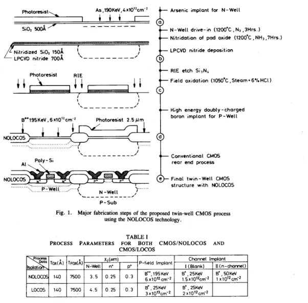
The major fabrication steps of the developed twin-well CMOS process are shown in Fig. 1. The n-well was initially 141,
PI.
Manuscript received November 9, 1988; revised April 19, 1989. H.-H. Tsai and C.-L. Yu are with the Institute of Electronics, National Chiao-Tung University, Hsinchu, Taiwan, Republic of China, and the IC Development Center, Electronics Research and Service Organization (ERSO), Industrial Technology Research Institute (ITN), Hsinchu, Taiwan, Republic of China.
C.-Y. Wu is with the Institute of Electronics, National Chiao-Tung University, Hsinchu, Taiwan, Republic of China.
IEEE Log Number 8929027.
formed by a high-energy (190 keV) arsenic ion implantation followed by a subsequent drive-in at 1200°C in an N2 ambient for 3 h, as shown in steps
8
and0.
After strippjng the sacrificed oxide (500A),
the thin pad oxide (150 A ) was grown and then nitridized in an ammonia ambient at 1200°C for 7 h which drove the n-well deeper.A LPCVD-Si3N4 layer (700
A)
was then deposited. Using a photolithographic step0,
the nitride and oxynitride layers were patterned for LOCOS oxidation. Note that a zero alignment key was used and the misalig!ment tolerance was about 0.3 pm. The field oxide (7500 A ) was grown in a pyrogenic steam ambient with 6-percent HC1 mixture and in- situ annealed to release the residual stress at the field oxide edge. Using a 2.5-pm-thick photoresist layer over the n-well region as an implantation mask, high-energy doubly charged boron ions (B++) with an energy of 195 keV and a dose of 6 x 10¹²/cm2 were implanted into the p-substrate region for both shallow retrograde p-well formation [6] and p-field threshold-voltage adjustment, as shown in step0.
Note that a punchthrough implant for an n-channel MOSFET under the same photoresist layer and a blanket implant after the removal of the photoresist were performed to adjust the channel threshold voltage. It is clearly seen that a mask layer for channel implant is eliminated. After the proper annealing steps and a sequence of conventional n+-doped poly-gate CMOS back-end processes, twin-well CMOS transistors with process parameters listed in Table I were fabricated, as shown in step0.
It should be noted that twin-well CMOS transistors using conventional CMOS process were also fabricated for compari- son. For the p-well, the channel surface concentrations of NOLOCOS and conventional LOCOS are 7 x 1 0 ' 6 / ~ m 3 and 6 x 10¹⁶/cm3, respectively. For the n-well, the channel surface concentrations of NOLOCOS and conventional LO- COS are 2.22 X 10'6/~m3 and 1.8 X 10¹⁶/cm3, respectively. The process parameters for both technologies are listed in Table I.111. DEVICE CHARACTERISTICS
The fabricated CMOS transistors using the NOLOCOS technology have been characterized and compared with those using the conventional LOCOS technology.
A. Effective Channel Width
Wmsk and the effective dimension loss of channel width
A W,,A We, = Wmask - 2 A Weff, where A Weff is mainly due 0741-3106/89/0700-0307$01.00 O 1989 IEEE
308 IEEE ELECTRON DEVICE LETTERS, VOL. 10, NO. 7, JULY 1989
LOCOS
As ,190KeV. 4x10’1cm-2 Arsenic implant for N-Well Photoresist\
sio* SOOA’ N-Well drive-in (1200’C , N 2 ,3Hrs.)
Nitridation of pad oxide (12OO0C, NH, ,7Hrs.) LPCVD nitride deposition
R E etch Si3NL
Field oxidation (1050°C, Steam+6% HCI)
High energy doubly -charged boron Implant for P - W e l l - _ _ I _ - - - - LPCVD nitride 700 B” 195 KeV , 6 x l 0” cm-2 Photoresist 2.5 p m, 140 7500 L . 5 0 25 0.3 25Kev
I
25KevI
3x10’3cm-Z 2xto’zcm-z \ Conventional CMOSt
rear end processx- - -
-
- - - -1’Poly - si
AI, \
Final twin -Well CMOS structure with NOLOCOS
NO
b
\. ... ... ... ::..!?.:.Me!!. ...<
N-Well ) b - - - , P-SubFig. 1. Major fabrication steps of the proposed twin-well CMOS process using the NOLOCOS technology.
TABLE I
PROCESS PARAMETERS FOR BOTH CMOS/NOLOCOS AND CMOSlLOCOS
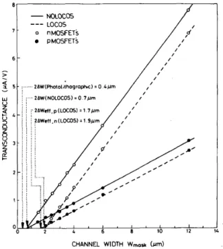
to the photolithographic process, reactive ion-etching process, bird’s beak length, and lateral diffusion of field implantation. Comparisons of the measured linear transconductances G,
between the NOLOCOS and the LOCOS for CMOS transis- tors with various channel widths are shown in Fig. 2. The effective channel-width improvements for both p- and n- MOSFET’s using the NOLOCOS are extracted to be 1 .O and
1.2 pm, respectively. Note that the dimensional loss due to bird’s beak length is less than 0.1 pm [2] and that due to lateral diffusion is only about 0.05 pm for both p-well and n-well regions. Therefore, the dimensional loss excluding the loss due to the photolithographic process (0.2 pm each side) is only 0.15 pm, which is consistent with that measured from the SEM cross-section view [2].
the other hand, the A V,, of those devices using the LOCOS are widely spread to more than 200 mV for Wmsk narrower than 3 pm. Under the back-gate bias of 3 V, the AV,, variations of both n- and p-MOSFET’s using the NOLOCOS are within 40 and 160 mV, respectively, while those devices using the LOCOS are widely spread to more than 400 mV for Wmsk narrower than 3 pm. The improvements on A V,h of n- MOSFET are due to the reduction of the lateral diffusion of p- field impurity using high-energy doubly charged B + + implan- tation, and those of p-MOSFET are due to the reduction of the lateral diffusion of n-field impurity using arsenic implantation instead of phosphorus for n-well doping.
C. Isolation Property
The subthreshold I- V characteristics ‘of the CMOS field
B. Threshold Voltage transistors with ( W / A ~ ) , , ~ = 30 pm/2 pm are shown in Fig.
The improvements of the narrow-width effects on the 4, in which the threshold voltages of both n- and p-channel threshold voltages of CMOS transistors using the NOLOCOS field MOS transistors are v t h f , , = 13.7 V and Vl,fp = - 18.3
are shown in Fig. 3. The threshold-voltage variations (A Vh) V, respectively. It is shown that the leakage current is in of both n- and p-MOSFET’s using the NOLOCOS are within subpicoamperes. Therefore, the field isolation of the NOLO-
TSAI et a/. : TWIN-WELL CMOS PROCESS USING NOLOCOS TECHNOLOGY 309 - Nococos LOCOS 0 nMOSFETs PMOSFETS ---
’-
2AWdf,p(LOC05)=1 7pm ?AWcff,n(LOCOS)=l 9prn ICHANNEL WIDTH Wmo* k m )
Fig. 2. Comparisons of the linear transconductances of CMOS transistors with various channel widths between NOLOCOS and conventional LOCOS isolation technologies. 8 00
-
600 E ? 6 Loo 2 > 200 > v > I 0 0-
> -2ci E a5
-1oi I n 5 > - 6ci -eo(?
I 1 I I p \ *Fig. 3. Comparisons of the narrow-width effects on the threshold voltage of CMOS transistors between NOLOCOS and conventional LOCOS isolation technologies.
-
nMOSFETiIVGSI ( v o l t s )
Fig. 4. Isolation property of CMOS field transistors fabricated using the NOLOCOS technology.
IV
.
CONCLUSIONA new twin-well CMOS process using the NOLOCOS technology has been developed. This novel CMOS process
with arsenic ion implantation for the n-well and doubly charged B + + ion implantation for the retrograde p-well is
shown to fully utilize the high-temperature NOLOCOS isola-
tion technology and eliminates one mask layer as compared to the conventional twin-well process. Through device character- ization, it has been shown that the developed twin-well CMOS
process using the NOLOCOS technology offers a fairly large
recovery of the effective channel width, very good device isolation properties, and very small narrow-width effects. These features are beneficial for scaled CMOS/VLSI fabrica-
tion.
REFERENCES
[I] J. A. Appels, E. Kooi, M. M. Paffen, J. J. H. Schatorji, and W. H. C. G. Veikuylen, “Local oxidation of silicon and its application in semiconductor device technology,” Philips Res. Rep., vol. 25, pp. [2] H.-H. Tsai, C.-L. Yu, and C.-Y. Wu, “A bird’s beak reduction technique for LOCOS in VLSI fabrication,” IEEE Electron Device Lett., vol. EDL-7, pp. 122-123, Feb. 1986.
H.-H. Tsai, S.-M. Chen, and C.-Y. Wu, “A new fully recessed-oxide (FUROX) field isolation technology for scaled VLSI circuit fabrica- tion,” IEEE EIectron Device Lett., vol. EDL-7, pp. 124-126, Feb.
1986.
H.-H. Tsai, C.-L. Yu, and C.-Y. Wu, “LOCOS enhancement using thermal nitridation technique,” in EIectron Devices MateriaIs Symp. (EDMS) (Taiwan, ROC), Sept. 1985, pp. 5-8.
[5] H.-H. Tsai, C.-L. Yu, and C.-Y. Wu, “The nitridized oxide-LOCOS (NOLOCOS) technology for scaled CMOSNLSI fabrication,” in Proc. Int. Symp. VLSI Technology, Syst. Application (Taipei, Taiwan, ROC), May 1987, pp. 324-328.
[6] R. A. Martin, A. G. Lewis, T. Y. Huang, and J. Y. Chen, “A new process for one micron and finer CMOS,” in IEDM Tech. Dig., 1985,
118-132, 1970.
[3]
[4]