234 IEEE ELECTRON DEVICE LETTERS, VOL. 30, NO. 3, MARCH 2009
Poly-Si Thin-Film Transistor Nonvolatile Memory
Using Ge Nanocrystals as a Charge Trapping
Layer Deposited by the Low-Pressure
Chemical Vapor Deposition
Po-Yi Kuo, Tien-Sheng Chao, Senior Member, IEEE, Jyun-Siang Huang, and Tan-Fu Lei
Abstract—We have successfully developed and fabricated a
poly-Si thin-film transistor (poly-Si TFT) nonvolatile memory us-ing Ge nanocrystals (Ge-NCs) as a charge trappus-ing layer. Process compatibility and memory operation of the device were inves-tigated. The Ge-NC trapping layer was directly deposited by low-pressure chemical vapor deposition at 370◦C. Results show that the new poly-Si TFT nonvolatile Ge-NC memory has good programming/erasing efficiency, long charge retention time, and good endurance characteristics. These results show that poly-Si TFT nonvolatile Ge-NC memory is the promising nonvolatile memory candidate for system-on-panel application in the future.
Index Terms—Charge retention, endurance, Ge nanocrystals
(Ge-NCs), nonvolatile memory, polycrystalline silicon thin-film transistors (poly-Si TFTs), programming/erasing.
I. INTRODUCTION
P
OLYCRYSTALLINE silicon thin-film transistors (poly-Si TFTs) are very attractive for system on panel (SOP) as device performance improves further [1]. The entire system will include memories, solar cells, and touch sensors as well as driver circuits for active-matrix liquid crystal displays [2]–[4].Nanocrystal (NC) floating-gate (FG) memories offer a num-ber of potential advantages over FG Flash devices, including improved scalability, retention, and cyclability, as well as lower voltage operation [5]. Recently, nonvolatile memory devices us-ing Ge or Si NCs (Ge-NCs or Si-NCs) as FG have been widely studied because of its excellent memory performance and high scalability. Ge has smaller bandgap and similar electron affinity compared with Si. Nonvolatile memory devices using Ge-NCs instead of Si-NCs have superior retention properties [6]–[11]. Most of the Ge-NC fabrication methods, including the
Manuscript received November 12, 2008; revised December 3, 2008. Current version published February 25, 2009. This work was supported by the National Science Council, Taiwan, under Contract NSC-97-2221-E-009-152-MY3. The review of this letter was arranged by Editor J. K. O. Sin.
P.-Y. Kuo, T.-S. Chao, and J.-S. Huang are with the Department of Electrophysics, National Chiao Tung University, Hsinchu 300, Taiwan (e-mail: [email protected]; [email protected]; jinshiang@ gmail.com).
T.-F. Lei is with the Department of Electronics Engineering and Institute of Electronics, National Chiao Tung University, Hsinchu 30010, Taiwan (e-mail: [email protected]).
Color versions of one or more of the figures in this letter are available online at http://ieeexplore.ieee.org.
Digital Object Identifier 10.1109/LED.2008.2011145
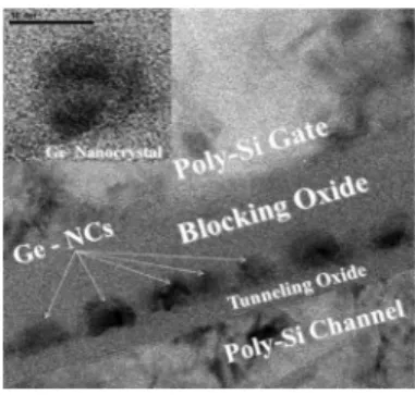
Fig. 1. Cross-sectional TEM microphotographs of poly-Si TFT nonvolatile Ge-NC memory. The blocking oxide and tunneling oxide thicknesses are about 40 and 10 nm, respectively. The sizes of the Ge-NCs are about 9–11 nm, and the density of the Ge-NCs is about 2−4 × 1011cm−2.
thermal annealing of Ge and dielectric mixture, the oxidation of SiGe, and Ge ion implantation, all require annealing at high temperature [6], [9], [11]. In this letter, a poly-Si TFT nonvolatile memory using Ge-NCs as a charge trapping layer (poly-Si TFT nonvolatile Ge-NC memory) was proposed. The Ge-NCs embedded in oxide were directly deposited by low-pressure chemical vapor deposition (LPCVD) at 370 ◦C, and therefore, it was easy to control the real thickness of tunneling oxide. The size of Ge-NCs can be easily modified by changing the deposition time and flow rate of GeH4[10].
II. EXPERIMENT
Fig. 1 shows the cross-sectional transmission electron mi-croscope (TEM) microphotographs of poly-Si TFT nonvolatile Ge-NC memory. First, a 100-nm amorphous silicon (a-Si) active region layer was deposited by LPCVD at 550◦C on wet oxide and then was crystallized by solid phase crystallization at 600◦C for 24 h. After the active region patterning, a 10-nm tetraethoxysilane (TEOS) tunneling oxide layer was deposited by LPCVD. After deposition of a-Si nuclei, the Ge-NCs were directly deposited by LPCVD at 370◦C. The a-Si nuclei were deposited by using SiH4 as a gaseous precursor at 550 ◦C on tunneling SiO2 surface. This way, we were able to adjust the a-Si nuclei density, and hence, the density of the Ge-NCs can be between 109 cm−2 and slightly less than 1012 cm−2. Once the a-Si nuclei were deposited, we stopped the SiH4gas 0741-3106/$25.00 © 2009 IEEE
KUO et al.: POLY-Si TFT MEMORY USING Ge-NCs AS A CHARGE TRAPPING LAYER DEPOSITED BY THE LPCVD 235
flow. After cooling down CVD chamber temperature to 370◦C, GeH4 was introduced to selectively grow Ge-NCs on the a-Si nuclei. This way, the a-Si nuclei were not oxidized because they were never exposed to oxygen. Indeed, no Ge-NCs would grow on oxidized a-Si nuclei [10]. The size of Ge-NCs can be easily controlled by changing the deposition time and flow rate of GeH4. The low deposition temperature of Ge-NCs is suitable for low-temperature poly-Si TFT applications. A high-resolution image of one typical Ge-NC is shown in Fig. 1 for revealing the geometrical and crystal characteristics of the Ge-NC. In NC nonvolatile memories, the size of NC is an important factor that affects electrical characteristics. The size of Ge-NC embedded in oxide should not be scaled below 5 nm, because the quantum confinement effect becomes very signifi-cant for such small Ge-NC [12], [13]. Large quantum confine-ment leads to the conduction band in the NC being much higher than that of the Si substrate, resulting in enhanced leakage from NC and shorter retention time [6].
Next, a 40-nm TEOS blocking oxide layer and a 200-nm a-Si gate layer were deposited in sequence. After gate implantation and defining gate electrode, a self-aligned implantation was used to form the n+ S/D. After passivation process, dopants were activated by furnace at 600 ◦C for 12 h. After contact and metallization processes, NH3 plasma treatments were im-plemented after sintering at 400◦C for 30 min.
III. RESULTS ANDDISCUSSION
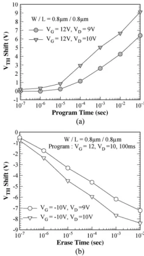
Fig. 2 shows the measured (a) programming and (b) eras-ing characteristics of poly-Si TFT nonvolatile Ge-NC mem-ory with W/L = 0.8 μm/0.8 μm. We employ channel hot electron injection to program and also band-to-band tunneling induced hot-hole injection (BTBHHI) to erase. The program conditions are as follows: VG= 12 V and VD= 9, 10 V. The
erase conditions are as follows: VG=−10 V and VD= 9,
10 V. We can read the threshold voltage (VTH) shift (= VTH of program state–VTH of erase state) from Fig. 2. We think that VTH shift is due to the electron trapping in the Ge-NC trapping layer. With increasing the VD, the VTH shift also increases and the programming/erasing speeds become faster. In the floating-body poly-Si TFTs, we apply appropriate drain voltages before strong drain avalanche. These drain voltages are used to achieve good channel hot electron injection efficiency in the programming and good BTBHHI efficiency in the erasing. The applied drain voltage can be reduced with decreasing gate length [14], [15].
Fig. 3 shows the measured retention characteristics at 85◦C. The poly-Si TFT nonvolatile Ge-NC memory exhibits good retention characteristics at high temperature due to the suf-ficiently deep trapping level of Ge-NCs. Compared with Si, Ge has a narrower bandgap and a similar electron affinity. Nonvolatile memory devices using Ge-NCs instead of Si-NCs have superior retention properties. Here, we display real VTH shift instead of normalized VTHshift. The normalized VTHshift will change with different VTH shift at 0 s. For example, the normalized VTH shift of large VTH shift state (∼7.8 V) at 0 s is about 15%, but the normalized VTHshift of small VTHshift state (∼4.4 V) at 0 s is about 25%.
Fig. 2. Measured (a) programming and (b) erasing characteristics of poly-Si TFT nonvolatile Ge-NC memory with W/L = 0.8 μm/0.8 μm.
Fig. 3. Measured retention characteristics at 85◦C. The poly-Si TFT non-volatile Ge-NC memory was programmed to two VTHshift states at 0 s.
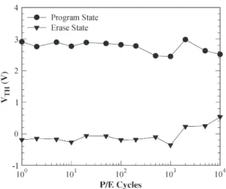
The measured endurance characteristics are shown in Fig. 4. We find that the memory window narrowing rate slightly in-creases after 2× 10³ P/E cycles for the memory with 10-nm tunneling oxide. It may be due to the stress-induced electron traps generated in the tunneling oxide during P/E cycles. Thick tunnel oxide has more serious memory window closure. Thus, the tradeoff between retention and endurance characteristics shall be carefully conducted [16]. We believe that retention and endurance characteristics can be significantly improved
236 IEEE ELECTRON DEVICE LETTERS, VOL. 30, NO. 3, MARCH 2009
Fig. 4. Measured endurance characteristics. The memory window narrows to about 2.1 V after 104P/E cycles.
by using high-quality tunneling oxide and blocking oxide. Furthermore, it is important to effectively reduce the amount of grain boundaries in the channel for achieving high-performance poly-Si TFT nonvolatile memory.
IV. CONCLUSION
In this letter, poly-Si TFT nonvolatile Ge-NC memory has been reported and demonstrated. The Ge-NCs embedded in oxide were directly deposited by LPCVD at 370 ◦C, and therefore, it was easy to control the real thickness of tunneling oxide. The low deposition temperature of Ge-NCs is suitable for low-temperature poly-Si TFT applications. Experimental results show that the poly-Si TFT nonvolatile Ge-NC memory has good P/E efficiency, long charge retention time, and good endurance characteristics. The poly-Si TFT nonvolatile Ge-NC memory has high potential in realizing the nonvolatile memory for SOP application in the future.
ACKNOWLEDGMENT
The authors would like to thank the Nano Facility Cen-ter (NFC) of National Chiao Tung University and the Na-tional Nano Device Laboratory (NDL) for providing process equipment.
REFERENCES
[1] A. J. Walker, S. Nallamothu, E. H. Chen, M. Mahajani, S. B. Herner, M. Clark, J. M. Cleeves, S. V. Dunton, V. L. Eckert, J. Gu, S. Hu, J. Knall, M. Konevecki, C. Petti, S. Radigan, U. Raghuram, J. Vienna, and M. A. Vyvoda, “3D TFT-SONOS memory cell for ultra-high density file storage applications,” in VLSI Symp. Tech. Dig., 2003, pp. 29–30. [2] J. H. Oh, H. J. Chung, N. I. Lee, and C. H. Han, “A high-endurance
low-temperature polysilicon thin-film transistor EEPROM cell,” IEEE
Electron Device Lett., vol. 21, no. 6, pp. 304–306, Jun. 2000.
[3] N. D. Young, G. Harkin, R. M. Bunn, D. J. McCulloch, and I. D. French, “The fabrication and characterization of EEPROM arrays on glass using a low-temperature poly-si TFT process,” IEEE Trans. Electron Devices, vol. 43, no. 11, pp. 1930–1936, Nov. 1996.
[4] M. Cao, T. Zhao, K. C. Saraswat, and J. D. Plummer, “A simple EEPROM cell using twin polysilicon thin film transistors,” IEEE Electron Device
Lett., vol. 15, no. 8, pp. 304–306, Aug. 1994.
[5] K. W. Guarini, C. T. Black, Y. Zhang, I. V. Babich, E. M. Sikorski, and L. M. Gignac, “Low voltage, scalable nanocrystal FLASH memory fabricated by templated self assembly,” in IEDM Tech. Dig., 2003, pp. 541–544.
[6] J. H. Chen, Y. Q. Wang, W. J. Yoo, Y. C. Yeo, G. Samudra, D. SH Chan, A. Y. Du, and D. L. Kwong, “Nonvolatile flash memory device using Ge nanocrystals embedded in HfAlO high-κ tunneling and control oxides: Device fabrication and electrical performance,” IEEE Trans. Electron
Devices, vol. 51, no. 11, pp. 1840–1848, Nov. 2004.
[7] B. H. Koh, E. W. H. Kan, W. K. Chim, W. K. Choi, D. A. Antoniadis, and E. A. Fitzgerald, “Traps in germanium nanocrystal memory and effect on charge retention: Modeling and experimental measurements,” J. Appl.
Phys., vol. 97, no. 12, pp. 124 305-1–124 305-9, Jun. 2005.
[8] M. Kanoun, A. Souifi, T. Baron, and F. Mazen, “Electrical study of Ge-nanocrystal-based metal-oxide-semiconductor structures for p-type nonvolatile memory applications,” Appl. Phys. Lett., vol. 84, no. 25, pp. 5079–5081, Jun. 2004.
[9] Y. C. King, T. J. King, and C. Hu, “MOS memory using germanium nanocrystals formed by thermal oxidation of Si1−xGex,” in IEDM Tech. Dig., 1998, pp. 115–118.
[10] T. Baron, B. Pelissier, L. Perniola, F. Mazen, J. M. Hartmann, and G. Rolland, “Chemical vapor deposition of Ge nanocrystals on SiO2,” Appl. Phys. Lett., vol. 83, no. 7, pp. 1444–1446, Aug. 2003.
[11] H. I. Hanafi, S. Tiwari, and I. Khan, “Fast and long retention-time nano-crystal memory,” IEEE Trans. Electron Devices, vol. 43, no. 9, pp. 1553– 1558, Sep. 1996.
[12] M. She and T. J. King, “Impact of crystal size and tunnel dielectric on semiconductor nanocrystal memory performance,” IEEE Trans. Electron
Devices, vol. 50, no. 9, pp. 1934–1940, Sep. 2003.
[13] Y. M. Niquet, G. Allan, C. Delerue, and M. Lannoo, “Quantum con-finement in germanium nanocrystals,” Appl. Phys. Lett., vol. 77, no. 8, pp. 1182–1184, Aug. 2002.
[14] M. H. Chi and A. Bergemont, “Programming and erase with floating-body for high density low voltage flash EEPROM fabricated on SOI wafers,” in
Proc. IEEE Int. SOI Conf., 1995, pp. 129–130.
[15] M. Valdinoci, L. Colalongo, G. Baccarani, G. Fortunato, A. Pecora, and I. Policicchio, “Floating body effects in polysilicon thin-film transistors,”
IEEE Trans. Electron Devices, vol. 44, no. 12, pp. 2234–2241, Dec. 1997.
[16] Y. H. Lin, C. H. Chien, T. H. Chou, T. S. Chao, and T.-F. Lei, “Low-temperature polycrystalline silicon thin-film flash memory with hafnium silicate,” IEEE Trans. Electron Devices, vol. 54, no. 3, pp. 531–536, Mar. 2007.