具預先增強與準位自動校正之驅動電路
58
0
0
全文
(2) 具預先增強與準位自動校正之驅動電路 A Self-Calibrate Driver with Pre-Emphasis. Student : Kuan-Yu Chen. 研 究 生:陳冠羽. Advisor : Chau-Chin Su. 指導教授:蘇朝琴 教授. 國 立 交 通 大 學 電機與控制工程研究所 碩士論文. A Thesis Submitted to Department of Electrical and Control Engineering College of Electrical Engineering and Computer Science National Chiao Tung University in partial Fulfillment of the Requirements for the Degree of Master in Electrical and Control Engineering July 2005 Hsinchu, Taiwan, Republic of China. 中華民國九十四年七月.
(3) 具預先增強與準位自動校正之驅動電路. 研究生 : 陳冠羽. 指導教授 : 蘇朝琴 教授. 國立交通大學電機與控制工程研究所. 摘. 要. 由於製程技術的進步,CMOS 積體電路的操作頻率及電路複雜度也隨著增加。使得晶 片內部的邏輯閘以及連結外部的輸入/輸出介面之間的頻寬差距到達嚴重的比例。因此,連 接晶片之間的傳輸通道時常限制了系統的效能,這些系統包括網路的切換器、路由器、處 理器和記憶體之間的介面及多處理器的傳輸通道。 在此論文中,我們將簡單的介紹高速序列傳收機。我們提出一個可增強高頻區段訊號 的預先增強電路,使資料在接收端能在操作頻率下維持一定值。接著,我們再加上自我校 正功能,可以對輸出電壓準位做自動的調整,以防止製程漂移或溫度變化而造成輸出準位 的誤差。再者,我們可以決定近端電阻與驅動電路的等效阻值使其輸出阻抗接近 50 歐姆, 進而減少反射所造成的影響,實現此電路技術及設計概念也將再論文中說明。 論文中,我們將實現一個符合低電壓差動訊號標準 3.125 Gbps 的傳送器。此傳送器是 使用台積電 0.18µm CMOS 製程製作且在 1.8V 的供應電壓下其功率消耗為 50 毫瓦。 關鍵字: 高速串列鏈結,低電壓差動訊號標準,預先增強,自我校正.
(4) A Self-Calibrate Driver with Pre-Emphasis. Student: Kuan-Yu Chen. Advisor: Chau-Chin Su. Department of Electrical and Control Engineering National Chiao Tung University. Abstract Due to the scale-down of the process technologies, the operating frequency and circuit complexity of CMOS VLSI increase significantly. The growing gap between on-chip and off-chip I/O bandwidth is reaching the critical proportions. Therefore, the interconnections between chips often limit the performance of a system in applications such as network switches, routers, processor-memory interfaces, and multi-processor interconnects. For this reason, to integrate high speed serial links on chips can reduce the pin/wire count and power budget of a system significantly. In this thesis, we will introduce a high-speed serial link. We will propose the pre-emphasis circuit that can enlarge the high frequency components, so the overall frequency response at the receiving end is uniform across the operation frequency. Then we add the self-calibration function to our driver so that it can calibrate itself automatically to deal with process or temperature variation. In order to reduce the reflection effect, we can determent the termination resistor value of near end and the equivalent resistors of the driver to make these resistors be equal to 50 Ω in steady state. The circuit design will be described in detail. In this thesis, a 3.125 Gbps transmitter has been designed. It is compatible with the LVDS standard. In a TSMC 0.18-µm 1P6M CMOS technology, the transmitter circuit consumes 50mW on a 1.8V power supply. Keyword: High-speed serial link, LVDS, Pre-emphasis, Self-Calibrate.
(5) 致. 謝. 首先最要感謝的是我的指導教授 蘇朝琴教授,這兩年來各方面的教導,不論在生活或 學術上,都讓我有很多的收穫。 再來要感謝的是兩年來陪我走過學校生活的學長:鴻文、丸子與 totoro,在我想不出 東西時,總是一起 555,5 到地老天荒,活化頭腦,讓思維更加靈活;還有瑛佑、cgu 和 A-da 一起無聊"練瘋話"打嘴砲,另外還有仁乾、aming、小冠、匡良、智琦、楙軒、宗諭、順 閔…等等的學長同學們,大家一起運動烤肉讓我的兩年碩班生活過的充實。 最後當然是要感謝我的家人-父親、母親、姐姐和弟弟,沒有他們在背後的鼓勵,也不 會有今天的我,在此表示最誠心的感謝,感謝他們也感謝我生命中所有的人。. 陳冠羽 2005/7/27.
(6) List of Contents. List of Contents List of Contents ............................................................................V List of Tables................................................................................VI List of Figures.............................................................................VII Chapter 1 Introduction............................................................... 1 1.1 CMOS HIGH-SPEED SERIAL LINKS ..................................................................................... 1 1.2 MOTIVATION....................................................................................................................... 3 1.3 THESIS ORGANIZATION ....................................................................................................... 3. Chapter 2 Background study .................................................... 5 2.1 SIGNALING TECHNIQUES .................................................................................................... 5 2.2 CHANNEL LOSS.................................................................................................................. 7 2.3 TRANSMITTER PRE-EMPHASIS ............................................................................................ 8. Chapter 3 The Transmitter Architecture................................. 13 3.1 INTRODUCTION ................................................................................................................ 13 3.2 FUNCTIONAL BLOCKS ....................................................................................................... 14 3.3 SUMMARY........................................................................................................................ 28. Chapter 4 Transmitter Circuit Design ....................................... 29 4.1 INTRODUCTION ................................................................................................................ 29 4.2 CIRCUIT DESIGN .............................................................................................................. 30 4.3 SIMULATION RESULT ........................................................................................................ 40 4.4 IMPLEMENTATIONS ........................................................................................................... 44 4.5 SUMMARY........................................................................................................................ 46. Chapter 5 Conclusion ................................................................ 47 5.1 CONCLUSION ................................................................................................................... 47. Bibliography................................................................................ 48.
(7) List of Tables. List of Tables TABLE 4-1 TRUTH TABLE OF FSM .................................................................................33 TABLE 4-2 PARAMETER SUMMARY AFTER CALIBRATION................................................42 TABLE 4-3 CHIP SUMMARY OF THE TRANSMITTER .........................................................45.
(8) List of Figures. List of Figures FIGURE 1.1 BASIC LINK COMPONENTS: THE TRANSMITTER, THE WIRE, AND THE RECEIVER ............................................................................................................2 FIGURE 2.1 A POINT-TO-POINT, LOW SWING, INCIDENT-WAVE SYSTEM .............................6 FIGURE 2.2 FREQUENCY DEPENDENCE OF CHANNEL LOSS ...............................................7 FIGURE 2.3 PULSE RESPONSE OF A 1.5-METER PCB TRACE .............................................8 FIGURE 2.4 SIGNALING WAVEFORM (A) WITHOUT PRE-EMPHASIS (B) WITH 1-TAP PRE-EMPHASIS ....................................................................................................9 FIGURE 2.5 (A) THE INPUT SIGNAL IN TRANSMITTER, OUTPUT SIGNAL IN RECEIVER (B) WITH CHANNEL LOSS EFFECT, (C) WITH 1-TAP PRE-EMPHASIS ......................10 FIGURE 2.6 BLOCK DIAGRAM OF A PRESHAPING PARALLEL TRANSMITTER FOR MIT GROUP [10] ....................................................................................................... 11. FIGURE 2.7 BLOCK DIAGRAM OF A PRE-SHAPING PARALLEL TRANSMITTER FOR STANFORD GROUP [4] ....................................................................................... 11 FIGURE 2.8 TRANSMITTER BLOCK DIAGRAM [9]............................................................12 FIGURE 3.1 THE OVERALL TRANSMITTER ARCHITECTURE .............................................14 FIGURE 3.2 FREQUENCY RESPONSE, (A) THE HIGH FREQUENCY IS AMPLIFIED AND (B) THE LOW FREQUENCY IS ATTENUATED...............................................................15 FIGURE 3.3 (A) THE PRE-SHAPED SIGNAL IN THE TRANSMITTER, (B) INCREASING CURRENT OF THE FIRST TAP ...............................................................................16 FIGURE 3.4 EYE DIAGRAM OF THE RECEIVER, (A) OVER COMPENSATION FOR STEADY STATE WITH 1-TAP OF A SYMBOL SPACE (B) RISING TIME IS INCREASED WITH NON OVER COMPENSATION (C) COMPARISON BETWEEN (A) AND (B).............................................................................................................17 FIGURE 3.5 PROPOSED PRE-EMPHASIS FUNCTION ..........................................................17 FIGURE 3.6 EYE DIAGRAM OF THE PROPOSED PRE-EMPHASIS FUNCTION .......................18 FIGURE 3.7 DRIVER ARCHITECTURE : MAIN, CALIBRATION DRIVER AND PRE-EMPHASIS ..................................................................................................18 FIGURE 3.8 SIGNAL WAVEFORM WHEN TAP1 IS OPERATED .............................................19 FIGURE 3.9 TAP2 FUNCTION ..........................................................................................20 FIGURE 3.10 THE SIMULATION RESULT IN RECEIVER END (A) ONLY TAP1 (B) TAP1 AND TAP2 ..........................................................................................................20 FIGURE 3.11 TRANSITION DETECTOR FUNCTION ............................................................21 FIGURE 3.12 SIMULATION RESULT OF THE TRANSITION DETECTOR ................................21 FIGURE 3.13 THE DRIVER EQUIVALENT MODEL .............................................................22 VII.
(9) List of Figures. FIGURE 3.14 STATE DIAGRAM .......................................................................................23 FIGURE 3.15 CALIBRATION CURVE ACCORDING TO STATE DIAGRAM ..............................23 FIGURE 3.16 THE CALIBRATION CURVE (A) TT CASE (B) SS CASE (C) FS CASE (D) SF CASE ............................................................................................................27 FIGURE 3.17 CASES THAT CAN NOT BE CALIBRATED (A) Rd < Rstable (B) Ru < Rstable (C) Ru < Rstable AND Rd < Rstable .........................................27 FIGURE 4.1 FREQUENCY RESPONSE OF USING HSPICE CHANNEL MODEL .....................29 FIGURE 4.2 TAP1 DETECTION CIRCUIT ...........................................................................30 FIGURE 4.3 TAP2 DETECTION CIRCUIT ...........................................................................30 FIGURE 4.4 THE ARCHITECTURE OF THE SWING CALIBRATION CONTROLLER .................31 FIGURE 4.5 THE COMPARATOR CIRCUIT (A) FOR HIGHER OUTPUT VOLTAGE (B) FOR LOWER OUTPUT VOLTAGE ..................................................................................32 FIGURE 4.6 THE SHIFT REGISTERS .................................................................................34 FIGURE 4.7 REFLECTION EFFECT WHEN CALIBRATION FUNCTION OPERATES..................34 FIGURE 4.8 SOLUTION OF REFLECTION EFFECT..............................................................34 FIGURE 4.9 SIMULATION RESULT OF CALIBRATION WHICH OVERCOMES REFLECTION EFFECT ..............................................................................................................35 FIGURE 4.10 THE ARCHITECTURE OF THE COUNTER ......................................................35 FIGURE 4.11 THE FUNCTION VERIFICATION OF THE COUNTER ........................................36 FIGURE 4.12 SIMPLIFIED ELECTRICAL MODEL OF CHIP-PACKAGE INTERFACE ................36 FIGURE 4.13 LVDS DRIVER (A) TRADITIONAL (B) PROPOSED DRIVER ...........................37 FIGURE 4.14 COMPLETE VERSION OF OUR DRIVER (A) MAIN AND CALIBRATION DRIVER (B) PRE-EMPHASIS DRIVER ....................................................................38 FIGURE 4.15 EQUIVALENT RESISTORS CHANGE .............................................................39 FIGURE 4.16 THE OUTPUT VOLTAGE OF THE TT, SS AND FF CASES ...............................39 FIGURE 4.17 DELAY BUFFER CIRCUIT ............................................................................40 FIGURE 4.18 POST-SIMULATION RESULTS OF CALIBRATION FUNCTIONS (A) TT CASE (B) SS CASE (C) SF CASE (D) FS CASE (E) FF CASE. ..........................................42 FIGURE 4.19 EYE DIAGRAM OF PROPOSE TRANSMITTER WITHOUT PRE-EMPHASIS .........43 FIGURE 4.20 EYE DIAGRAM OF PROPOSE TRANSMITTER WITH PRE-EMPHASIS ...............43 FIGURE 4.21 OVERLAP EYE DIAGRAMS TO COMPARISON ...............................................44 FIGURE 4.22 LAYOUT OF PROPOSED TRANSMITTER .......................................................45. VIII.
(10) Chapter 1 Introduction. Chapter 1 Introduction. 1.1 CMOS High-Speed Serial Links Traditionally, high-speed serial links in Gbps range are implemented in GaAs or bipolar technologies. The primary advantage of those technologies is the faster intrinsic device speed (higher fT ). However, CMOS technology is more widely available and allows higher integration than other technologies. Recently development has shown that CMOS is capable of achieving Gbit/s data rate[1,2] Another motivation for CMOS implementation is the faster improvement of CMOS speed than the speed of other technologies due to the rapid scaling of it feature sizes. 0.18 µm CMOS technologies have speed comparable to a 0.5um GaAs technology. Although it is always possible to yield inherently better devices in non-transitional technologies, the momentum and investment in CMOS technology development is progressing toward making CMOS the fastest technology[3].. 1.
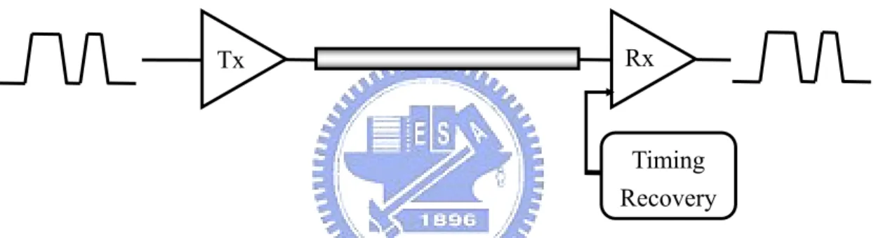
(11) Chapter 1 Introduction. The standards for high-speed link are either over short distance in copper cable or long distances in optical fiber. The high bandwidth is provided by optical fiber over a lot long distances. But the optical fiber and necessary components also cost a lot. The optical links are not the only solution for high-speed communication over long distances. It is cheaper solution for high-speed communication to use cooper cables to replace optical fiber. But the length limits the bandwidth of cooper cable. Hence, cooper links, which are focus of this thesis, are usually used for short distance application, such as system-to-system interconnections in same room[4]. A typical link is comprised of three primary components: a transmitter, a channel, and a receiver. The transmitter converts digital bits into a signal stream that is propagated on the channel to the receiver. The receiver converts this analog signal back into binary data. Figure 1.1 shows the configuration.. Rx. Tx. Timing Recovery Figure 1.1 Basic link components: the transmitter, the wire, and the receiver A transmitter sends the data as analog quantities. The analog values are simply either a HIGH-level or LOW-level to represent a single bit, known as non-return-to-zero (NRZ). For example, in an optical system, they are the levels of different amounts of optical power. For electrical systems, these levels are of different signal voltages. The channel is the medium where the data is propagated. This medium can be an optical fiber, a coaxial cable, an unshielded twisted-pair, a printed-circuit board (PCB) trace, or the chip package. Channel can attenuate or filter signal and introduce noise. It is difficult to overcome the attenuation and noise from the channel in transceiver design while transmitting high data rate. To recover the signal from transmitter, the analog waveform is amplified and sampled. In order to recover the high-speed data, the receiver circuit has to be able to determine the high-speed small inputs from transmitter correctly. The time-recovery 2.
(12) Chapter 1 Introduction. circuit properly places the sampling strobe.. 1.2 Motivation Advances in IC fabrication technology have led to an exponential growth of the speed and integration levels of digital IC’s. The bandwidth has increased the demand for higher inter-chip communication to maximize overall system performance. There are two approaches to high-speed signaling, parallel buses and serial links. For parallel buses, many buses are implemented in a system to increase the signaling bandwidth. But the large buses increase the system e.g. cost, power consumption, and complexity. For serial links, it is to maximize the communication bandwidth and distance in a signal cable. Serial links offer a high-speed and low-cost solution to multi-gigabit per second rates over long distance. Applications such as computer-to-computer or computer-to-peripheral interconnection are several meters. In this thesis, we will implement a system architecture which uses non-return-to-zero (NRZ) signaling techniques. A novel pre-emphasis circuit is proposed. A 3 Gbps transmitter with pre-emphasis to compensate loss of channels has been designed. A self-calibration function has been also implemented to compensate process and environmental variation.. 1.3 Thesis organization The thesis organization is described as follows: Chapter 2: We will describe the basics of the high-speed link and channel analysis. We also introduce the basics concept of pre-emphasis. Chapter 3: We will introduce the proposed transmitter architecture and explain the pre-emphasis method to overcome the limited channel bandwidth. We will also introduce self-calibration concept and algorithm in this chapter to deal with process variation. Chapter 4: We will discuss the detail circuit design of the transmitter. Also, a novel pre-emphasis circuit and a self-calibration circuit are proposed. The implementation of the function blocks of the transmitter is also described in this. 3.
(13) Chapter 1 Introduction. chapter. Finally the overall simulation results are summarized at the end. Chapter5: The research is concluded in this chapter.. 4.
(14) Chapter 2 Background Study. Chapter 2 Background Study. 2.1 Signaling Techniques This section describes two different approaches to high-speed signaling in digital systems. The first method is traditional high-swing signaling, such as TTL or CMOS. They have been used in most computer systems in the past years, especially for chip-to-chip communication. This conventional method limits the speed to 100MHz. The frequency is difficult to be scaled with improving process technology. As the speed in the modern digital system increases, the conventional method is, therefore, becoming a major bandwidth bottleneck. The second method is discussed in this thesis. The point-to-point incident-wave signaling does not suffer from the limitation of the conventional method. So its data rate can be scaled with the process technology. The new signaling technique is emerging in high-speed systems due to the scaling.. 5.
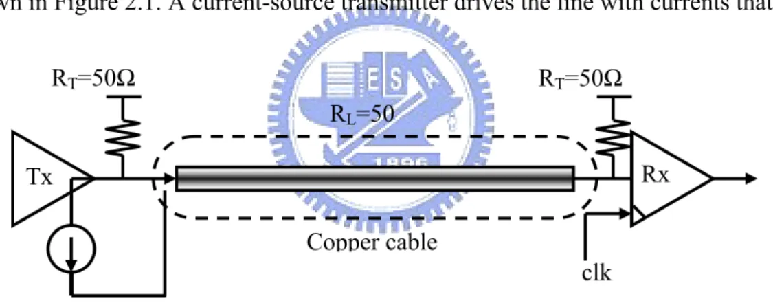
(15) Chapter 2 Background Study. 2.1.1 Traditional Large-Swing Signaling Traditional signaling systems are limited to data rates of about 100Mb/s per wire or less and dissipate large energy per bit transmitted and signaling rates do not scale with the improvement in the process technology. Many modern microprocessors operate their external buses at a small fraction of the internal clock rate due to the limitations. In traditional CMOS systems, a CMOS inverter is used both as the driver and receiver. The cable usually has a characteristic impedance of 50Ω to 100Ω. These signaling systems are slow because the high impedance driver is unable to switch the line voltage completely on the incident wave [5].. 2.1.2 Point-to-Point Low-Swing Signaling A signaling system that overcomes the limitations of traditional signaling is shown in Figure 2.1. A current-source transmitter drives the line with currents that RT=50Ω. RT=50Ω RL=50 Rx. Tx Copper cable clk. Figure 2.1 A point-to-point, low swing, incident-wave system typically range from a couple of milliamperes to tens of milliamperes, resulting in a voltage swing range of 100mV to about 1V. The cable is terminated at both ends in its characteristic impedance. The receiver termination absorbs the incident wave, preventing any reflections. The source termination makes the systems more tolerant of crosstalk and impedance discontinuities. A high-gain clocked regenerative receiver amplifier can be both low offset (~30-60mV) and high gain. With the improved receivers with low offset and high sensitivity, this system can operate reliably using very small swings. Therefore this signaling method also offers a considerable reduction in power dissipation of the system. The system described can also operate at data rates independent of the line 6.
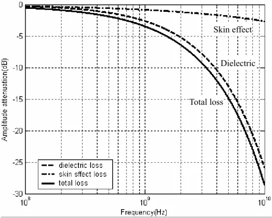
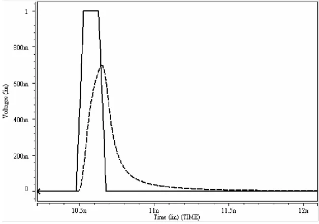
(16) Chapter 2 Background Study. length. A new symbol can be driven onto the line before the previous symbol arrives at the receiver. This results in a system whose data rate, to a first approximation, scales linearly with the device speed[4].. 2.2 Channel Loss The approximate channel frequency response in dB accounting for both skin effect and dielectric loss is given by [5], H ( f ,l )dB = −( hs ⋅. f + hd ⋅ f ) ⋅ l. (2.1). where l is the length of the channel, hs and hd are the skin effect and dielectric loss coefficients respectively.. Skin effect. Dielectric. Total loss. Figure 2.2 Frequency dependence of channel loss Figure 2.2 shows the frequency response of a channel, with both skin-effect and dielectric loss components shown separately. The amplitude reduces 3 dB at 0.9 GHz. Figure 2.3 shows the response of the channel for a 200ps 1V pulse with 50 ps rise time. The attenuation reduces the pulse amplitude by more than 30%. Moreover, 7.
(17) Chapter 2 Background Study. lower frequency attenuation results in the signal’s long setting tail. The long setting tail can cause significant inter-symbol interference (ISI). When signal bandwidth above 0.9 GHz, a channel pre-emphasis or equalizer is needed in the transmitter or receiver [4]. The pre-emphasis or equalizer functions as a complementary high pass filter to counter the channel attenuation.. Figure 2.3 Pulse response of a 1.5-meter PCB trace. 2.3 Transmitter Pre-emphasis 2.3.1 Transmit filter Transmitter preshaping usually uses a symbol-space finite impulse response (FIR) filter integrated into the output main driver. It can be specified by the following equation:. V0 ( n ) = Vi ( n ) − a1 ⋅ Vi ( n − 1 ) − a 2 ⋅ Vi ( n − 2 ) − ....... − a N ⋅ Vi ( n − N ). (2.2). The inputs are the present and past transmitted symbols. The coefficients of the filter are dependent on the channel characteristics. The length of the filter N is 8.
(18) Chapter 2 Background Study. dependent on the number of past symbols which affect the present symbol. Hence, the output of the filter is the sum of the present symbol value and the past N symbols weighted value. Figure 2.4 (a) shows that there is no eye crossing because high frequency components are attenuated. We have to pre-shape signals in the transmitter to compensate for frequency response in order to get correct data. We can upper high frequency components to get good eye like Figure 2.4 (b).. (a). (b) Figure 2.4 Signaling waveform (a) Without pre-emphasis (b) With 1-tap pre-emphasis Figure 2.5 shows the injury to signals cause by channel loss and compensated by 1-tap pre-emphasis. The received voltage height is reduced by a channel with small loss. Hence, the goal of the pre-emphasis is to overcome channel loss effect.. (a) 9.
(19) Voltage. Chapter 2 Background Study. (b). (c) Figure 2.5 (a) The input signal in transmitter, output signal in receiver (b) with channel loss effect, (c) with 1-tap pre-emphasis. 2.3.2 Design Techniques of Pre-emphasis The first implementation of a N-tap transmit filter was implemented by Dally and Poulton [10]. In this architecture, all the FIR filter calculations are done by digital adders and a digital-to-analog converter (DAC) generates the output pulse. The architecture of this approach is shown for 5-tap filter in Figure 2.6. Driver parallelism is used to overcome the speed limitations of the process. The digital logic modules which have the present and the five previous bits calculate the amplitude of the current pulse that should be transmitted and each driver module is a 6-bit DAC to reduce the quantization error of the FIR filter This implementation incorporates a 4GHZ FIR pre-shaping filter into a differential transmitter and allows a serial channel to operate over copper wires a 4Gbps. 10.
(20) Chapter 2 Background Study. 5 Filter. 6. 6-b DAC φ9. 6. 6-b DAC. 5 Filter. ...... D0-9 400MHz. Filter. ...... 10. Distribute and retime. 5. 6. High-speed output 4 Gbps. 6-b DAC φ0. Figure 2.6 Block diagram of a preshaping parallel transmitter for MIT group [10] The second implementation shows in Figure 2.7 with completely analog technique to realize the pre-emphasis filter. In this technique, the FIR N-tap filter is integrated into each driver module of the parallel transmitter. Each module uses the present and N previous bits to generate the complete preshaped pulse over N+1 bit periods directly and independently of all previously transmitted symbols. The individually preshaped symbols are summed at the transmitter output in an analog fashion. This implementation has 4-PAM pre-emphasis driver, and it can achieve 10Gbps over a pair of 10-meter PE142LL coaxial cables.. D0-9. 1-b DAC 1-b tap 1-b tap 1-b tap. D0. High-speed Output. ..... Low-speed. Distribute and retime. D9. 1-b FIR driver. Figure 2.7 Block diagram of a pre-shaping parallel transmitter for Stanford group [4] The third implementation shows in Figure 2.8. Pre-emphasis is implemented with the help of two auxiliary DACs (NDAC and PDAC). While active, PDAC generates a current proportional to the present symbol value. Similarly, NDAC generates a current of opposite polarity, proportional to the previous symbol. In this way, a pre-emphasis pulse is generated that is proportional to the change in the 11.
(21) Chapter 2 Background Study. transmit code, but without any digital computation. The reference current for NDAC and PDAC, as well as the pre-emphasis pulsewidth are programmable. The magnitude of the pre-emphasis current can be increased to compensate for greater attenuation over longer channels. This allows the transceiver to communicate over a range of track and cable lengths.. NDAC Z-1. Rmatch. Pulse Generator. clk. TX_data<2:0>. Pulse Generator PDAC TXDAC. Figure 2.8 Transmitter block diagram [9]. 12.
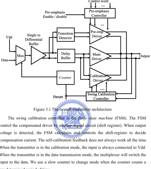
(22) Chapter 3 The Transmitter Architecture. Chapter 3 The Transmitter Architecture. 3.1 Introduction This chapter describes the proposed transmitter for a 3.125-Gbps serial link. This architecture contains a single to differential buffer, a controlled pre-driver module, a main driver, a self-calibrate mechanism, and a pre-emphasis module. In Figure 3.1, the multiplexer select Vdd or data to send to single-to-differential buffer which converts single ended data to differential ones. The top signal path is for pre-emphasis driver, the bottom one is for calibration driver and the middle one is for main driver. The top signals pass to the transition detector to detect whether signals transit or not. The transition detector decides to emphasize signals with transitionl. Besides, the output level is not guaranteed to have an expected voltage level due to the process variation or layout mismatch. So the controllable LVDS drivers can increase the output driver current to compensate the output voltage swing through the calibration driver as shown in Figure 3.1. 13.
(23) Chapter 3 The Transmitter Architecture. Control word … Pre-emphasis Controller. Pre-emphasis Enable / disable. … Single to Differential Buffer. Vdd. Mux Data. Transition Detector. Pre-emp Driver. Delay Buffer. Main Driver. Counter. Output. Calibration Driver. … Swing Calibration Controller. Reset. Figure 3.1 The overall transmitter architecture The swing calibration controller is the finite state machine (FSM). The FSM control the compensated driver by another digital circuit (shift register). When output voltage is detected, the FSM calculates and controls the shift-register to decide compensation current. The self-calibration feedback does not always work all the time. When the transmitter is in the calibration mode, the input is always connected to Vdd. When the transmitter is in the data transmission mode, the multiplexer will switch the input to the data. We use a slow counter to change mode when the counter counts a pre determined period of time.. 3.2 Functional Blocks We will discuss the important functional blocks in this section.. 3.2.1 Pre-Emphasis Module As described in chapter 2, the transmission line is a low pass function. Pre-emphasis circuit plays a role of high pass function so that the frequency response is flatten within the bandwidth of our desired frequency range in the receiver. This 14.
(24) Chapter 3 The Transmitter Architecture. frequency response can be written as H c ( f ) ⋅ H pre ( f ) = cons tan t. f ≥ f op ,. (3.1). where H c ( f ) is the channel frequency response, H pre ( f ) is the pre-emphasis frequency response and f op is the maximal operation frequency. The pre-emphasis either amplify the high frequency component or attenuate the low frequency component as shown in Figure 3.2 [8]. In the diagram, the dotted line means the overall frequency response. Gain. Pre-emphasis Channel frequency response. Freq.. (a). Gain. Channel frequency response Pre-emphasis. Freq. (b) Figure 3.2 Frequency response, (a) the high frequency is amplified and (b) the low frequency is attenuated. We use the scheme of Figure 3.2(a). The primary reason is that the low frequency component is attenuated and the voltage swing may not be large enough to recover data correctly at far end. This method increases the power of high frequency components. In order to increase the high frequency part, we can shape the transition of the signaling.. 15.
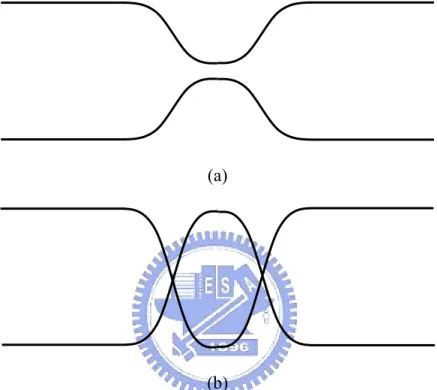
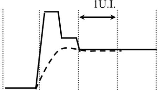
(25) Chapter 3 The Transmitter Architecture. Traditionally, a tap of the pre-emphasis is a symbol space as shown in Figure 3.3 (a). The dashed line is the waveform of the receiver. There are some problems. We can not compensate the rising (falling) time and the steady state voltage level simultaneously. In many specifications, the rising (falling) time is requested. The first tap of the pre-emphasis decides the rising (falling) time. In order to reduce rising time in the receiver, the first tap has to increase more current to enhance the output voltage of the transmitter as shown in Figure 3.3 (b). 1U.I.. (a). 1U.I.. (b) Figure 3.3 (a) The pre-shaped signal in the transmitter, (b) increasing current of the first tap We can also see that there is an overshot waveform at far end. In the receiver eye diagram, the overshot waveform is the over compensation for steady state voltage level as shown in Figure 3.4(a). If we only compensate for steady state voltage level and no overshot waveform in the receiver, the rising time may not short enough to match the specifications as shown in Figure 3.4(b). So we propose a new method to implement the pre-emphasis function as shown in Figure 3.5. A tap of the pre-emphasis which is only half symbol space is a feasible method to compensate for rising (falling) time and steady state voltage level simultaneously. If the first tap that controls the rising time is a symbol space, it may cause overshot waveform in the receiver. If we reduce it to half symbol space, the 16.
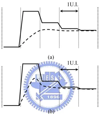
(26) Chapter 3 The Transmitter Architecture. overshot waveform is diminished and the rising (falling) time can be also compensate to match the specification. In Figure 3.6, we can see that the overshot waveform is diminished in the receiver and the rising (falling) time can be easily controlled with increasing current by the first tap. Therefore, our new method of the pre-emphasis function is better than traditional one in overcoming the channel loss effect.. Rising time 90ps. (a). Rising time 126ps. (b). (c) Figure 3.4 Eye diagram of the receiver, (a) over compensation for steady state with 1-tap of a symbol space (b) rising time is increased with non over compensation (c) comparison between (a) and (b) 1U.I.. Figure 3.5 Proposed pre-emphasis function 17.
(27) Chapter 3 The Transmitter Architecture. Transmitter Output. Receiver Input. Figure 3.6 Eye diagram of the proposed pre-emphasis function. 3.2.2 Pre-emphasis and Main Drivers The architectures of pre-emphasis, main driver and calibration driver are almost the same. There is an advantage to implement by similar architecture. Because of the similar architecture, the pre-emphasis driver, main driver and calibration driver have the same delay time.. Main driver D-. D+ a. Pre-emphasis tap1. a Ph-. Ph+ out b. outb. b Po-. Po+ Pre-emphasis tap2 c. c D+. DCalibration driver. Figure 3.7 Driver architecture : main, calibration driver and pre-emphasis 18.
(28) Chapter 3 The Transmitter Architecture. The driver includes the circuit blocks of the main driver, calibration driver and pre-emphasis as shown in Figure 3.7. The strength of each tap is decided by channel length and channel loss. The relationship between current (I) and differential amplitude of the output of the transmitter ( ∆V ) is. ∆V = I ⋅ Re. (3.2). where Re is the equivalent resistance. From Equation (3-2). We know that the amplitude increases with current or Re . In out system, Re is constant because of the termination resistance. The main driver represents the circuit of the original driver, the calibration driver represents the calibration circuit to calibrate output voltage level ( ∆V ) and pre-emphasis represents the pre-shaping circuit to emphasize the high frequency components. The function of tap1 is shown in Figure 3.8. The circuit of tap1 operates when a data transition is detected and it supplies I 1 to enlarge ∆V . 1U.I. out. outb. Tap1 in operation Figure 3.8 Signal waveform when Tap1 is operated Tap1 is used to any transition and it only controls slew rate. So we need another tap to deal with the steady voltage level. Tap2 is essential in our design. Tap3 is required or not is determined by the receiver sensitivity, the area, and the loading overhead. In out system, if we have three tap, every tap is one third symbol space. It is a challenge to out design. So we only have two taps in our system. The function of the tap2 is shown in Figure 3.9.. 19.
(29) Chapter 3 The Transmitter Architecture. 1U.I. out. outb. Tap2 in operation Figure 3.9 Tap2 function Figure 3.10(a) is the simulation that only tap1 operates. We can see that the data is attenuated after transition. The tap2 circuit supplies enough current to compensate for attenuation as shown in figure 3.10(b).. (a). (b) Figure 3.10 The simulation result in receiver end (a) only tap1 (b) tap1 and tap2 20.
(30) Chapter 3 The Transmitter Architecture. The calibration driver provides current in initial state to compensation the output amplitude according to FSM that we will discuss later.. 3.2.3 Transition Detector The transition detector detects data transition. When data has a transition, it sends a pulse to the pre-emphasis driver to make the pre-emphasis increases current to compensate attenuation as shown in Figure 3.11. in inb. Tap1. Tap2 1U.I. Figure 3.11 Transition detector function. Tap1. Tap2. Figure 3.12 Simulation result of the transition detector When data is from high to low or low to high, the transition detector produces two types of pulses for pre-emphasis and calibration as shown in Figure 3.12.. 21.
(31) Chapter 3 The Transmitter Architecture. 3.2.4 Swing Calibration Controller In out system, the driver is like a voltage divider with resistors as shown in Figure 3.13. vdd. vdd I Ru. Ru out. outb Re. Rd. Rd. Figure 3.13 The driver equivalent model In (3.2), the current (I) is equal to. I=. vdd Ru + Rd + Re ,. (3.3). and (3.2) can be rewritten to. ∆V =. Re ⋅ vdd Ru + Rd + Re .. (3.4). We can write Vout and Voutb. Vout =. Rd + Re ⋅ vdd Ru + Rd + Re. Rd Voutb = ⋅ vdd Ru + Rd + Re. (3.5). So when we change Ru and Rd , Vout and Voutb are both influenced at the same time. If the process variation happens, we can control and change Ru and Rd by parallel resistors. The FSM is needed here. This FSM can control how many resistors are parallel connected to guarantee the output swing. The state diagram of 22.
(32) Chapter 3 The Transmitter Architecture. FSM is shown in Figure 3.14. Reset No / turn on One more. Yes Vout > Vrefh No. PMOS. No. Vout > Vrefh. Voutb < Vrefl. Voutb < Vrefl. Yes. No / turn on One more NMOS. Yes Stop. Figure 3.14 State diagram In Figure 3.14, Vrefh and Vrefl are the reference voltages. Vrefh is lower than. Vout , and Vrefl is higher than Voutb . So we can control the output amplitude by changing Vrefh and Vrefl . According to state diagram, we can plot our calibration curve as shown in Figure 3.15.. ∆VH ( n −1 ). Vrefh. ∆VHn VHn. VH ( n −1 ). Vout. Voutb. ∆VL( n −1 ). Vrefl. ∆VLn VL( n −1 ). VLn. Figure 3.15 Calibration curve according to state diagram How can we guarantee the algorithm to be convergent and calibrates the output voltages to the wanted levels by control the parallel resistors? If we can prove following equations (3.6), (3.7), and (3.8), we can say this algorithm is convergent because Vout and Voutb are monotonic increasing and monotonic decreasing. Lim V Hn= V DD ; Lim V Ln= 0. (3.6). V Hn> V H ( n − 1 ) ;V Ln< V L( n − 1 ). (3.7). n→∞. n→∞. 23.
(33) Chapter 3 The Transmitter Architecture. ∆V Hn< ∆V H ( n − 1 ) ; ∆V Ln< ∆V L( n − 1 ). (3.8). Where V Hn is the nth voltage level of V out , and V Ln is the nth voltage level of. V outb . V Hn and V Ln are the voltages that are parallel connection with n resistors ( R Hn and R Ln ). R Hn and R Ln are. R Hn =. Ra ⋅ Ru ; n ⋅ R H + Ra. (3.9). Rb ⋅ Rd R Lm = m ⋅ R L + Rb. where Ra and Rb are the parallel resistors and n is the number of the parallel resistors. We can easily prove Equation (3.6) is correct.. R Lm + Re ⋅ V DD = V DD n → ∞ R Hn + R Lm + Re. Lim V Hn= Lim. n→∞. m→∞. (3.10). R Lm Lim V Ln= Lim ⋅ V DD = 0 n→∞ n → ∞ R Hn + R Lm + Re m→∞. Afterward we will show that Equation (3.7) is correct. In Figure 3.15, V Ln and VL( n −1 ) are given by. R Ln ⋅ V DD R Hn + R Ln + Re R L( n − 1 ) V L( n − 1 ) = ⋅ V DD R H ( n − 1 ) + R L( n − 1 ) + Re V Ln =. (3.11). We can suppose that R u is equal to Rd and Ra is equal to Rb and n is equal to m, so R Hn is equal to R Lm . This supposition makes calculation easily. We can get the Equation (3.12) after reduction. VL( n −1 ) − VLn =. ( RH ( n −1 ) − RH ) ⋅ Re ( RH ( n −1 ) + RL( n −1 ) + Re ) ⋅ ( RHn + RLn + Re ) 24. ⋅ VDD > 0. (3.12).
(34) Chapter 3 The Transmitter Architecture. And in the same way, we also show that V H ( n − 1 ) is greater than V Hn . So we prove Equation (3.7) is correct. Then we will discuss Equation (3.8). ∆V Hn and ∆V H ( n − 1 ) in Figure 3.15 are the differences between high level and low level of V out . They are given by. ∆V Hn=. ( RL( n −1 ) − RLn ) ⋅ RHn ( RHn + RL( n −1 ) + Re ) ⋅ ( RHn + RLn + Re ). ∆V H ( n −1 )=. ⋅ VDD. ( RL( n − 2 ) − RL( n −1 ) ) ⋅ RH ( n −1 ) ( RH ( n −1 ) + RL( n −1 ) + Re ) ⋅ ( RH ( n −1 ) + RL( n − 2 ) + Re ). (3.13). ⋅ VDD. If ∆V H ( n − 1 )− ∆V Hn> 0 , then ∆V H ( n − 1 )> ∆V Hn . So we can get the below equation.. ∆V H ( n −1 )−∆V Hn= ( −. ( RL( n − 2 ) − RL( n −1 ) ) ⋅ RH ( n −1 ) ( RH ( n −1 ) + RL( n −1 ) + Re ) ⋅ ( RH ( n −1 ) + RL( n − 2 ) + Re ). ( RL( n −1 ) − RLn ) ⋅ RHn ( RHn + RL( n −1 ) + Re ) ⋅ ( RHn + RLn + Re ). (3.14). ) ⋅ VDD. We can also suppose that R u is equal to Rd and Ra is equal to Rb , so R Hn is equal to R Ln and n is equal to m. In this way, we can calculate easily. Because it is long and complex calculation, the reader can try to calculate and we do not show the process here. After reduction, we know that Equation (3.14) is greater than zero so. ∆V H ( n − 1 ) is greater than ∆V Hn . And in the same way, we can show that ∆V L( n − 1 ) is greater than ∆VLn . Above the demonstration, we know that Equation (3.6), (3.7), and (3.8) are all correctly. So this algorithm is stable and convergent and. Vout and Voutb are monotonic increasing and monotonic decreasing. There are calculations by hand to demonstrate that this algorithm feasible. We get the values of R u , Rd , Ra and Rb in spice simulation under all corner cases and plot calibration curves after calculation as shown in Figure 3.16. The reader may find FF case is mission. Because it matches the output voltage in initial state, the FSM will not operate calibration function. 25.
(35) Chapter 3 The Transmitter Architecture. 1.06 1.02. Voltage (V). 0.98 0.94 0.9 0.86 0.82 0.78 0.74 0.7. (0,0) (1,0) (1,1) (2,1) (2,2). (3,2). (a). Number of parallel resistor (Ra,Rb). 1.06 1.02. Voltage (V). 0.98 0.94 0.9 0.86 0.82 0.78 0.74 0.7. (0,0) (1,0) (1,1) (2,1) (2,2). (3,2) (3,3) (4,3) (4,4) (5,4) Number of parallel resistor (Ra,Rb) (b). 1.06 1.02. Voltage (V). 0.98 0.94 0.9 0.86 0.82 0.78 0.74 0.7. (0,0) (1,0) (1,1) (2,1). (c). 26. Number of parallel resistor (Ra,Rb).
(36) Chapter 3 The Transmitter Architecture. 1.06 1.02. Voltage (V). 0.98 0.94 0.9 0.86 0.82 0.78 0.74 0.7. (0,0). (0,1) (1,1) (1,2) (2,2). (d). Number of parallel resistor (Ra,Rb). Figure 3.16 The calibration curve (a) TT case (b) SS case (c) FS case (d) SF case We will discuss some cases that can not be calibrated perfectly by this algorithm. Our driver is like a resistor system as shown in Figure 3.13. If R u or Rd is less than Rstable (the resistor value for the desired level) in the initial state, what is happen in this status. Figure 3.17 shows the results of the above the problem. If R u or Rd is less than Rstable in the initial state, then only one voltage of output will be calibrated and the other one will not be calibrated as shown in Figure 3.17 (a) (b). (a). (b). (c) Figure 3.17 Cases that can not be calibrated (a) Rd < Rstable (b) Ru < Rstable (c) Ru < Rstable and Rd < Rstable 27.
(37) Chapter 3 The Transmitter Architecture. The same status happens, when R u and Rd are less than Rstable in the initial state. The calibration function does not work and the voltage levels of the output are determined by initial resistors as shown in Figure 3.17(c). When R u and Rd are greater than Rstable , the FSM will calibrate both voltage levels of the output. This is an initial condition for this algorithm. Note that parallel resistor only increases and not decrease.. 3.3 Summary In this chapter, the architecture of the proposed transmitter is described. The pre-emphasis concept is introduced. In the next chapter, we will describe the detail circuit. The algorithm of calibration is proposed and proven that it is convergent. We will realize this algorithm by circuit in the next chapter.. 28.
(38) Chapter 4 Transmitter Circuit Design. Chapter 4 Transmitter Circuit Design. 4.1 Introduction This chapter will describe the detail circuit of the proposed architecture. The circuit includes the pre-emphasis transition detector, the output swing calibration controller, and the driver circuit. At the end of this chapter, the simulation results are given. We use the channel in SPICE to test and verify the proposed architecture. The frequency response of channel is shown in Figure 2.2.. Figure 4.1 Frequency response of using HSPICE channel model 29.
(39) Chapter 4 Transmitter Circuit Design. Figure 4.1 shows the frequency response using the HSPICE model. The characteristic impedance of the channel is 50 Ω .. 4.2 Circuit Design 4.2.1 Transition Detector Chapter3 has described the function of the 2 taps pre-emphasis. Tap1 operates when there are data transitions. The tap1 detection block is as shown in Figure 4.2. We use latch to produce a data delay of half symbol space. Then this circuit provides opposite pulses by using NAND gate and NOR gate. Pout1-0 and Poutb1-0 send pulses when data transit from high to low and Pout0-1 and Poutb0-1 send pulses when data from low to high.. in. latch. Pout1-0 latch Poutb0-1. clkb. clk. Poutb1-0. latch inb. latch Pout0-1 Figure 4.2 Tap1 detection circuit. in. Pout_O1-0. latch. clk. latch. latch. clkb. clk. latch inb. Poutb_O0-1 Poutb_O1-0. latch. latch Pout_O0-1. Figure 4.3 Tap2 detection circuit 30.
(40) Chapter 4 Transmitter Circuit Design. The tap2 detection block is shown in Figure 4.3. Tap2 operates when there are data transitions and it maintains the voltage level of the output after tap1 is over. We also use latch to make delay and use logic gate to generate pulses. Pout_O1-0 and Poutb_O1-0 send pulses when data is from high to low and Pout_O0-1 and Poutb_O0-1 send pulses when data is from low to high. Note that the clock rate of the transition detector is the same as the data rate. For example, data rate is 3Gbps and the clock rate is 3GHz.. 4.2.2 Swing Calibration Controller Swing calibration controller is used to compensate voltage of the output due to process variation. This block includes FSM, a shift register, and comparators as shown in Figure 4.4.. u. FSM_P. qu. d. D. Q. clk u. 1020mV. Shift register. 1. s0u. …. Vout. EnableP. s11u. EnableN. s0d. 12. 0. d. Voutb. 0. Shift register s11d. 1. d u. …. gnd. 780mV. clkb. 12 Calibration driver. FSM_N qd. D. Q. Figure 4.4 The architecture of the swing calibration controller The source information of FSM is from the comparators. We use a simple two-stage operational amplifier to compare the output voltage and reference voltages as shown in Figure 4.5. Inverters are added to obtain digital outputs.. 31.
(41) Chapter 4 Transmitter Circuit Design. VDD. Vout. Vrefh. U. Vrefl. D. Vbias. (a) VDD. Vbias. Voutb. (b) Figure 4.5 The comparator circuit (a) for higher output voltage (b) for lower output voltage After the comparison with output voltage level and reference voltage, we have two digital outputs (U and D). When Vout is higher than Vrefh , U is 1, otherwise U is 0. When Voutb is lower than Vrefl , D is 1, otherwise D is 0.. According to results of. the comparators and Figure 3.14, we can find the truth table and equations of FSM as shown in Table 4-1. 32.
(42) Chapter 4 Transmitter Circuit Design. Table 4-1 Truth table of FSM udq 000 001 010 011 100 101 110 111. qu qd Pmos Nmos 0 0 setup 1 1 setup 1 0 1 0 0 1 0 1 0 0 stable stable 0 0 stable stable. qu = u ⋅ ( d + q ) qd = d ⋅ ( u + q ). (4-1). This calibration begins when there is a reset signal. Vout that is a higher DC voltage level is calibrated first, when calibration function operates. Vout is calibrated until u is one. It means Vout is higher than Vrefh . When FSM calibrates Vout , we use. qu to control the multiplexer to transmit clock to shift register. It makes shift register work. When qu is one, it means Vout is less than Vrefh and we need to increase resistors to raise Vout . Increasing one resistor means the shift register shifts one to next. When qu is zero, it means Vout has been greater than Vrefh and the shift register stops working and holds the value in the shifter register. When Vout is. V calibrates over, FSM begins to calibrate outb and it is the same process we describe the above-mentioned. But we use clkb to achieve. This way can reduce calibration cycle time. Two calibration functions will operate in rotation until qu and qd are all zero and calibration is over. It means Vout is greater than Vrefh and Voutb is less than Vrefl . Figure 4.6 shows the show the shift register. We can see that the shift registers always shift right. So the shift registers increase the number of one and do not reduce. The flip-flop of shift registers is the static type. We can not use the dynamic flip-flop, because after the self-calibration the output value of the D flip-flop must hold on itself forever.. 33.
(43) Chapter 4 Transmitter Circuit Design. Vdd. D Q. D Q. D Q. D Q. D Q. D Q. .... .... Enablep s0u Vdd. s2u. s1u. D Q. D Q. s8u D Q. D Q. s10u. s9u. D Q. s11u D Q. ........ Enablen s0d. s1d. s2d. s8d. s9d. s10d. s11d. Figure 4.6 The shift registers When calibration function operates, the reflection will happen. The reflection makes calibration function error and unlock as shown in Figure 4.7.. Vout No reflection effect Reflection effect Voutb. Figure 4.7 Reflection effect when calibration function operates In order to solve this problem, we reduce the clock rate to wait for the reflection effect to disappear and sample the stable output as shown in Figure 4.8. Shift register working time. Clk. Waiting time. Waiting time. Figure 4.8 Solution of reflection effect This solution has successfully solved the reflection effect. The simulation results as shown in Figure 4.9. When output voltage is stable, we send a pulse to EnableP (EnableN).. 34.
(44) Chapter 4 Transmitter Circuit Design. Vout Voutb EnableP EnableN Clk. Figure 4.9 Simulation result of calibration which overcomes reflection effect. 4.2.3 Counter The counter is a simple block. The counter operates at low as kHz. So we choose the simple architecture shown in Figure 4.10. There are six D Flip-Flops and a NOR gate. D and Qb are connected to together so that D Flip-Flops become T-Flip-Flops. When the clock trigger, S1~S6 are triggered in sequence. After 16 clocks, Tx goes high, the calibration process ended and the driver starts sending data. D Clk. Q. D. rst Qb S0. Q rst Qb. D S1. Q. D. Q rst Qb. rst Qb S2. Q. D S3. D. rst Qb. Q rst Qb. S4. S5. Figure 4.10 The architecture of the counter Figure 4.11 shows the function verification of the counter above. After the reset, S0~S4 begin to count until S5 changes. Tx signal rise from LOW to HIGH and hold on until the next reset. We use this counter to decide when the transmitter to transmit or do self-calibration. Tx signal presents the operation mode of our transmitter.. 35. Tx.
(45) Chapter 4 Transmitter Circuit Design. clk reset S0 S1 S2 S3 S4 S5 stable. Tx. Figure 4.11 The function verification of the counter. 4.2.4 Driver The driver is studied in this section. The power supply and ground of an IC is not ideal. It is combined with the equivalent inductance and capacitance of power distribution networks as shown in Figure 4.12. The load capacitor will be charged and discharged when signal transient. The switching noise increases as the frequency increases. VDD. CVdd. LVdd. Lpin. Cpad. CVss. CL. LVss. Figure 4.12 Simplified electrical model of chip-package interface. 36.
(46) Chapter 4 Transmitter Circuit Design. Conventionally, two current sources are connecting to power and ground respectively to minimize the current change hence reduce noise as shown in Figure 4.13 (a). Unfortunately, these two current sources will create a large voltage drop and limit the output voltage swing. In order to meet LVDS standard, the size of the four switching transistors need to be increased. So, the sizes of the pre-drivers must also be increased. This will increase the area and power of the pre-driver. It is a trade-off between the performance and the cost. Due to the device size scaled-down, the power supply voltage decreases. This problem becomes a challenge for designers. So, we proposed the following architecture. It has no current source in power supply and ground as shown in Figure 4.13 (b).. (a) (b) Figure 4.13 LVDS driver (a) traditional (b) proposed driver This methodology has some advantages. First, the driver needs no current source so output signal swing is enlarged. It also reduces the sizes of switch transistor greatly. Hence, the sizes of the pre-driver are reduce as well. It reduces the overall chip area substantially. Furthermore, the whole driver architecture looks like the two inverter connected back to back, it makes the control and layout easier. Notice that, the common-mode voltage is lowered from 1.25V to 0.9V to be used in a 1.8V supply environment. According to the proposed driver, we add logic gates to the driver. The completive version for the design is shown in Figure 4.14. Figure 4.14 (a) shows the circuit of the main driver and the calibration driver. 37.
(47) Chapter 4 Transmitter Circuit Design. For the main driver, A and B pins are connected to Vdd. For calibration driver, then we can control A and B pins according to the swing calibration controller. In total, there are twelve calibration drivers. Figure 4.14 (b) shows the circuit of the pre-emphasis driver. We can control A and B pins respectively to connect HIGH or LOW to determent how many PMOS and NMOS being turned on according to the channel loss. The transition detector controls Pout0-1, Poutb0-1, Pout1-0 and Poutb1-0. When data has transitions, the transition detector generates pulses to control these pins to shape output signal. Note that Tap1 and Tap2 are the same and the only difference is that the transition detector sends different widths of pulses to the drivers.. A. A. in. inb. B. B (a). A Pout0-1. A Poutb1-0. Pout1-0. Poutb0-1 B. B (b). Figure 4.14 Complete version of our driver (a) main and calibration driver (b) pre-emphasis driver In chapter3, we stated that our driver is like a voltage divider with resistors. These resistors are PMOSs and NMOSs as shown in Figure 4.14. And we will discuss the reflection problem. When the driver is operating in the pre-emphasis state, we can not guarantee that equivalent resistor is 50 Ω . But we hope it is 50 Ω to cancel the reflection effect in steady statue at least. We can determent the termination resistor value of near end and the equivalent resistors of four switches to make these resistors 38.
(48) Chapter 4 Transmitter Circuit Design. be equal to 50 Ω when the reflection happens as shown in Figure 4.15. When we determent termination resistor value of near end, we just control the output voltage at desired level, then the resistor will be equal to the needed 50 Ω . If the output voltage is wrong, the swing calibration controller will calibrate it. 1U.I. out. outb. Not 50 Ω. 50 Ω. Figure 4.15 Equivalent resistors change According to simulation results, we can get relationship between the turn-on MOSs and the output voltage in Figure 4.16. We can change tune-on MOS to change the output voltage to reach desired level. At the same method, the SF and FS cases also are considered in our driver design.. Figure 4.16 The output voltage of the TT, SS and FF cases. 39.
(49) Chapter 4 Transmitter Circuit Design. 4.2.5 Delay Buffer The delay buffer is the simple circuit. In order to obtain the same delay for the main driver, the calibration driver, and the pre-emphasis driver, we use inverter chains to obtain the same delay as shown in Figure 4.17.. in. latch. inb. latch. Main/calibration Driver. Figure 4.17 Delay buffer circuit. 4.3 Simulation Result 4.3.1 Output Swing Calibration Simulation To verify the design of the swing calibration controller circuit, the post-simulation results of the transmitter circuit are shown in this section. Figure 4.18 and Table 4-2 show the simulation results of the calibration function. We set the reference voltages to 1020mV ( V refh ) and 780mV ( V refl ) for a swing of 250mV and a common mode of 900mV. V high is 1025mV and Vlow is 775mV. The calibration needs at most twelve clock cycles to complete, our counter will count sixteen clock cycles and switch to transmission mode. We can see the mode change in Figure 4.18. The calibration function of FF case does not operate because R u and Rd are less than Rstable initially. R ru and Rrd can be calculated according to the simulation data and their values are about 50 Ω in steady state. This can reduce the reflection effect.. 40.
(50) Chapter 4 Transmitter Circuit Design. Vout. Voutb. (a). Vout Voutb. (b). Vout. Voutb. (c). Vout. Voutb. Calibration mode Transmission mode (d) 41.
(51) Chapter 4 Transmitter Circuit Design. Vout. Voutb. (e) Figure 4.18 Post-Simulation results of calibration functions (a) TT case (b) SS case (c) SF case (d) FS case (e) FF case. Table 4-2 Parameter summary after calibration Corner case. After Vhigh. Vlow. After. Reflection Reflection. Calibration Calibration resistor Ru Rd R ru. resistor Rrd. TT. 1.022V 0.768V 178.2 Ω 176.01 Ω 49.7 Ω. 49.9 Ω. FF. 1.025V 0.768V 175.8 Ω 174.3 Ω. 49.5 Ω. 49.7 Ω. SS. 1.023V 0.760V 171.5 Ω 167.7 Ω. 49.0 Ω. 49.3 Ω. FS. 1.036V 0.777V 171.2 Ω 173.3 Ω. 49.6 Ω. 49.2 Ω. SF. 1.034V 0.773V 170.6 Ω 172.2 Ω. 49.4 Ω. 49.3 Ω. 4.3.2 Output Eye Diagram Simulation After checking the calibration functions, we simulate the output eye diagram of our driver in this section. We use C language to generate 3.125Gbps random data. In Figure 4.19, the driver without the pre-emphasis has a jitter of 26ps in post-layout simulation. The height of the eye diagram is about ±250mV. Receiver eye diagram is not good due to channel loss. So we add pre-emphasis function to the driver and the output jitter is about 36ps as shown in Figure 4.20. Although the transmitter output jitter is increased, the eye diagram of the receiver is a better than in Figure 4.19. The height of the eye diagram of the receiver is about ±200mV. 42.
(52) Chapter 4 Transmitter Circuit Design. ~26ps. Tx output. Rx input. Figure 4.19 Eye diagram of propose transmitter without pre-emphasis. Tx output. ~36ps. Rx input. Figure 4.20 Eye diagram of propose transmitter with pre-emphasis Figure 4.21 is the overlap of the eye diagrams with and without pre-emphasis. We can see clearly that pre-emphasis compensates the channel loss effectively. 43.
(53) Chapter 4 Transmitter Circuit Design. Rx input (without Pre-emphasis). Rx input (with pre-emphasis). Figure 4.21 Overlap eye diagrams to comparison. 4.4 Implementations The proposed transmitter is implemented using TSMC 1P6M 0.18um. The total chip area is 0.95mm*0.84mm and the core area is 0.47mm*0.44mm as shown in Figure 4.22. The driver is in the middle of the chip and the transition detector (TD) and the swing calibration controller (SCC) are on both sides. We use pre-emphasis control pins to control pre-emphasis according to the channel response. Some pins are reserved for debugging. The summaries of post-layout simulation are shown in Table 4-3.. 44.
(54) Chapter 4 Transmitter Circuit Design. Vbias. Vbias. Vrefl. Vrefh. Debug control pin. gnd. vdd 840um. Figure 4.22 Layout of proposed transmitter Table 4-3 Chip summary of the transmitter Function. Tx with pre-emphasis. Technology. 0.18um 1P6M CMOS. Power Supply. 1.8V. Chip area. 940*850 (um2). Core area. 470*440 (um2). Transistor/Gate Count. 4221/1360. Power Dissipation. 38.7 mW (without pre-emp) 50.6 mW (with pre-emp). Jitter (pk-pk). 26p @3.125Gbps(no pre-emp) 36p @3.125Gbps(with pre-emp) 45. 950um. SCC. Pre-emp control pins. TD. SCC. Driver. TD. Pre-emp control pins. reset vin outb out clk clks.
(55) Chapter 4 Transmitter Circuit Design. 4.5 Summary In this chapter, we have described the proposed transmitter circuit. The driver has an additional circuit that can calibrate the output voltage by itself. The chip can detect the output level and start the calibration by reset. After 16 clocks, the calibration ends and the driver start sending data. The pre-emphasis is also added to this driver to compensate channel loss. According to the channel response, we can adjust pre-emphasis. We can control the rising/falling time and no over compensation in steady state. The overall simulation results of transmitter and receiver eyes diagrams and calibration are shown in this section.. 46.
(56) Chapter 4 Transmitter Circuit Design. Chapter 5 Conclusion. 5.1 Conclusion High-speed link becomes more and more important. In this thesis, we proposed a 3.125 Gbps transmitter architecture that uses novel scheme with self-calibration and pre-emphasis. We have described Tap1 and Tap2 of the pre-emphasis. It improves the signal quality at far end. The self-calibration that compensates the process variation is also proposed and its algorithm is proved. We have described overall transmitter circuit and simulation. According to post-layout simulation, we know that the self-calibration and pre-emphasis are working correctly. Our pre-emphasis is better than others, because we can control the rising (falling) time and no overshot in steady state. The proposed transmitter is composed of the digital logic gates, so a self-calibration, all-digital 3Gbps driver with pre-emphasis is implemented in this thesis. The proposed driver can be used in SATA Ⅱ [8]. This transmitter is implemented in TSMC 1P6M 0.18um CMOS technology.. 47.
(57) Chapter 4 Transmitter Circuit Design. Bibliography [1]. C.-K. K. Yang and M. A. Horowitz, "A 0.8um CMOS 2.5Gbps Oversampling Receiver and Transmitter for Serial Links," IIEEE Journal of Solid-Sate Circuits, vol. 12, pp. 2015-2023,Dec, 1996.. [2]. A. X. Widmer, K. Wrenner, H. A. Ainspan, et al., "Single-Chip 4 x 500-MBd CMOS Transceiver," IEEE Journal of Solid-Sate Circuits, vol. 31, pp. 2004-2014,Dec, 1996.. [3]. C.-K. K. Yang, Design of High Speed Serial Links in CMOS, PhD Dissertation, Stanford University, 1998. [4]. R. Farjad-Rad, A CMOS 4-PAM Multi-Gbps Serial Link Transceiver, PhD Dissertation, Stanford University, 2000. [5]. W. J. Dally and J. W. Poulton, Digital System Engineering: Cambridge University Press, 1998.. [6]. David K. Cheng, Fundamentals of Engineering Addsion-Wesley Publishing Company, New York, 1993. [7]. Chun-Hong Wang, “5Gbps Serial Link Transceiver with Pre-Emphasis” Master Degree dissertation of National Central University 2002. [8]. Serial ATA Workgroup “SATA: High Speed Serialized AT Attachment,” Revision 1.0, 26-May-2004.. [9]. D.J. Foley; M.P. Flynn;“A low-power 8-PAM serial transceiver in 0.5-μm digital CMOS”, Solid-State Circuits, IEEE Journal of , Volume: 37 , Issue: 3 , March 2002 Pages:310 – 316. [10]. W.J. Dally, J. Poulto, “Transmitter equalization for 4-Gbps signaling,” IEEE Micro, 1997.. [11]. Chih-Hsien lin; Chang-Hsiao Tsai; Chih-Ning Chen; Shyh-Jye Jou; “4⁄2 PAM serial link transmitter with tunable pre-emphasis” Circuits and Systems, 2004. ISCAS '04. Proceedings of the 2004 International Symposium on , Volume: 1 , 23-26 May 2004 Pages:I - 952-5 Vol.1. [12]. Geurts, T.; Rens, W.; Crols, J.; Kashiwakura, S.; Segawa, Y.; “A 2.5 Gbps 3.125 Gbps multi-core serial-link transceiver in 0.13um CMOS” Solid-State 48. Electromagnetics,.
(58) Chapter 4 Transmitter Circuit Design. Circuits Conference, 2004. ESSCIRC 2004. Proceeding of the 30th European , 21-23 Sept. 2004 Pages﹕487–490 [13]. Muthali, H.S.; Thomas, T.P.; Young, I.A.; “ A CMOS 10-Gb/s SONET transceiver” Solid-State Circuits, IEEE Journal of , Volume: 39 , Issue: 7 , July 2004 Pages:1026 – 1033. 49.
(59)
數據
+7
![Figure 2.7 Block diagram of a pre-shaping parallel transmitter for Stanford group [4] The third implementation shows in Figure 2.8](https://thumb-ap.123doks.com/thumbv2/9libinfo/8230416.170882/20.892.138.748.432.948/figure-diagram-shaping-parallel-transmitter-stanford-implementation-figure.webp)
![Figure 2.8 Transmitter block diagram [9]](https://thumb-ap.123doks.com/thumbv2/9libinfo/8230416.170882/21.892.175.730.285.736/figure-transmitter-block-diagram.webp)
相關文件
The difference resulted from the co- existence of two kinds of words in Buddhist scriptures a foreign words in which di- syllabic words are dominant, and most of them are the
2.1.1 The pre-primary educator must have specialised knowledge about the characteristics of child development before they can be responsive to the needs of children, set
develop a better understanding of the design and the features of the English Language curriculum with an emphasis on the senior secondary level;.. gain an insight into the
Promote project learning, mathematical modeling, and problem-based learning to strengthen the ability to integrate and apply knowledge and skills, and make. calculated
Wang, Solving pseudomonotone variational inequalities and pseudocon- vex optimization problems using the projection neural network, IEEE Transactions on Neural Networks 17
volume suppressed mass: (TeV) 2 /M P ∼ 10 −4 eV → mm range can be experimentally tested for any number of extra dimensions - Light U(1) gauge bosons: no derivative couplings. =>
Define instead the imaginary.. potential, magnetic field, lattice…) Dirac-BdG Hamiltonian:. with small, and matrix
• Formation of massive primordial stars as origin of objects in the early universe. • Supernova explosions might be visible to the most
