國 立 交 通 大 學
電子工程學系 電子研究所碩士班
碩 士 論 文
具獨立雙閘極之 P 型聚集模式多晶矽奈米線
電晶體的製作與特性分析
Fabrication and Characterization of
P-Type Accumulation-Mode Independent
Double-Gated Poly-Si Nanowire Transistors
研 究 生:吳俊鵬
指導教授:林鴻志 博士
黃調元 博士
具獨立雙閘極之 P 型聚集模式多晶矽奈米線
電晶體的製作與特性分析
Fabrication and Characterization of
P-Type Accumulation-Mode Independent
Double-Gated Poly-Si Nanowire Transistors
研 究 生:吳俊鵬
Student:Jiun-Peng Wu
指導教授:林鴻志 博士 Advisors:Dr. Horng-Chih Lin
h
指導教授:
黃調元 博士
Advisors:
Dr. Tiao-Yuan Huang
國 立 交 通 大 學
電子工程學系 電子研究所碩士班
碩 士 論 文
A Thesis
Submitted to Department of Electronics Engineering & Institute of Electronics College of Electrical and Computer Engineering
National Chiao-Tung University in Partial Fulfillment of the Requirements
for the Degree of Master of Science
in
Electronic Engineering February 2011
Hsinchu, Taiwan, Republic of China
i
具獨立雙閘極之 P 型聚集模式多晶矽奈米線
電晶體的製作與特性分析
研究生 :吳俊鵬 指導教授 : 林鴻志 博士
研究生 : 許家維 指導教授 :
黃調元 博士
國立交通大學
電子工程學系 電子研究所碩士班
摘要
在本篇論文中,我們成功製作出操作在聚集模式(accumulation mode, AcM)下,
具獨立雙閘極之 P 型多晶矽奈米線電晶體。此元件在通道中擁有高濃度的摻雜,
且由於具有極小的奈米線尺寸,因此閘極可以有效的控制並開關元件。另外,此
種元件的電性表現,包含基本特性以及次臨界特性,都將與操作在加強模式
(inversion mode, IM)下,具有無摻雜通道的傳統元件做個比較。
在整個多晶矽通道導通的情況下, AcM 元件明顯具有較 IM 元件大的電流驅
動力。此外,在兩個獨立閘極所提供多元操作的彈性下,我們將這兩種元件間不
同的傳導機制成功地做區隔,並利用 TCAD 的模擬結果來做驗證。其次,由於 AcM
元件所提供的表面空乏區使得實質閘極介電層厚度的增加,因此具有較差的短通
ii
效應對兩種元件的影響。最後,我們也發現在同樣的閘極驅動下,AcM 元件在閘
極氧化層與通道的接面上具有較小的垂直電場,且由於 AcM 元件的實質通道涵蓋
整個奈米線,使得載子受到表面粗糙與介面缺陷散射的影響較小,因此對於 AcM
iii
Fabrication and Characterization of
P-Type Accumulation-Mode Independent
Double-Gated Poly-Si Nanowire Transistors
Student : Jiun-Peng Wu Advisors : Dr. Horng-Chih Lin
Student : Jiun-Peng Wu Advisors :
Dr. Tiao-Yuan Huang
Department of Electronics Engineering and Institute of Electronics
National Chiao Tung University, Hsinchu, Taiwan
Abstract
In this thesis, we have successfully fabricated p-type accumulation-mode (AcM) independent double-gated poly-Si nanowire (NW) transistors which contain a high doping concentration in the channel and can be effectively turned off on account of the ultra-small feature size of NW. In addition, the electrical characteristics are well compared to the conventional devices with undoped channels which operate in the inversion mode (IM).
Owing to the current conduction through the whole channel, the Ion
characteristics are obviously better for the AcM devices, so do the output characteristics. Moreover, due to the flexibility in device operation by the two independent gates, the differences of conduction mechanisms between the two types of devices can be clarified, and are also confirmed by the TCAD simulation
iv
results. We also found that short channel effects (SCEs) are more severe for the AcM devices, which is ascribed to the additional effective oxide thickness (EOT) contributed by the surface depletion layer. The Gm characteristics are also
characterized and compared between the two types of devices, from which the influences of gate coupling effect for each device are well discussed. On the other hand, the AcM devices have a smaller electric field at the interface at the same gate overdrive, and the carriers also inherently suffer less from the scattering of the surface roughness and the interface traps on account of the whole channel conduction. Thus, the Gm degradation with increasing gate overdrive is more
v
Acknowledgement
時光飛逝,很快的,碩士生涯即將告一段落,曾經傻呼呼的以為念研究所跟大學差 不多,但自從進來實驗室後,才發現”研究”這兩字還真不是件容易的事。各種學習與 挑戰讓我在這一年多也成長了不少,我了解到做研究跟大學寫寫報告有著天壤地別的差 別,即便如今我即將要拿到了碩士文憑,但其實我知道,我離真正的做學問還是差了十 萬八千里。但這些日子下來,我主要學到的東西並不是學術知識,而是做事情的態度, 學習與研究就跟做人處事一樣,必須要誠實面對自己,挖掘自己的淺力並且勇敢面對問 題,這些才是我這段日子下來最大的收穫。 在 ADTL 的時光裡,我先要特別感謝兩位指導教授,林鴻志 教授以及黃調元 教授, 由於你們對於學生有著一定的堅持與把關,我才能有所收穫與成長,懂得去學習觀察問 題,找出問題。雖然有時做實驗會感到辛苦了點,但我還是非常開心能跟到兩位老師, 畢竟有你們,我才能真正在研究所學到該有的一些知識與態度,而不是來混一張文憑, 在這裡非常謝謝你們的指導。 另外,對於 ADTL 的所有夥伴,我最感謝的就是陳威臣學長,你是我研究所時期所 遇到的最大貴人,也因為有你帶我入門以及做實驗,我才能如此順利,也很感謝你每次 都願意聽我說一堆我自己都不太確定的分析與解釋,也會很好心的陪我一起想甚至找資 料並指導我,非常感謝你,沒有你,我不會有今天的小小成就。當然後期也很感謝林哲 民學長在模擬的幫忙,也感謝你在百忙之中還是願意指導我一些分析與研究。其他包含 徐行徽學長、蔡子儀學長、林政頤學長、郭嘉豪學長、李克慧學姐,也感謝你們的對我 所有的指導與幫忙! 回到 631 來,當然少不了一起奮鬥的夥伴們,歷樺、宇賢、同偉、 嘉文、段凱、崇名、孝雄,有你們在實驗室的陪伴與玩鬧,讓我在有時苦悶的實驗裡還 能有夥伴可以聊天並紓解壓力,也很希望你們接下來的實驗及論文都能順順利利,當然 還有一群可愛的碩一學弟妹們,相信有你們的加入,ADTL 會更有生氣與活力,未來也請 多多加油了! 另外,我最想感謝的是我的父母:吳雄鈴 先生、蔡勉 女士,以及我的姊姊,吳茗 萱 女士,沒有你們,沒有今天的我,我希望你們知道,我所做的一切努力,都是為了 你們,沒有你們,我不會有如此的好勝心以及積極的態度,一切只希望你們能夠幸福快 樂,不要為我而擔心。同樣的,我也希望你們能因為有我而引以為傲,是你們引領著我, 讓我想要為了你們而努力,想要讓你們感到有我而覺得開心與驕傲,非常感謝你們對我 的照顧與栽培! 最後,這篇碩士論文,我希望能分享給我已逝去的大學好友:陳昱錚,我們這輩子 沒有辦法一起去洛杉磯看球賽了,但我會連你的份一起努力,因為你不幸的消息,讓我 更加省思到人生苦短,更該積極努力,活在當下。願天上的你也能繼續過的這麼開心, 也希望你能讓我跟你分享此刻的小小榮耀。 吳俊鵬 誌於 風城交大 2011 年 3 月vi
Contents
Abstract (Chinese)……… i
Abstract (English)……… iii
Acknowledgement (Chinese)……… v
Contents……… vi
List of Figure Captions……… viii
Chapter 1 Introduction………... 1
1.1 Overview of Multiple-Gated and Poly-Si Nanowires Transistors……… 1
1.2 Overview of Accumulation-Mode Devices……… 3
1.3 Motivation………... 5
1.4 Organization of this Thesis………...……….. 6
Chapter 2 Device Fabrication and Measurement Setup……… 7
2.1 Device Fabrication and Process Flow……….. 7
2.2 Images of Fabricated Devices………. 8
2.3 Measurement Setup……….. 9
Chapter 3 Results and Discussion……… 11
3.1 Basic Electrical Characteristics….……….. 11
3.1.1 Transfer Curves……….. 11
3.1.2 Output Characteristics……….. 13
vii
3.2 Subthreshold Characteristics….……….. 15
3.2.1 Short Channel Effects……….. 15
3.2.2 Variation of Electrical Parameters……….. 18
3.3 Transconductance Characteristics….……….. 20
3.3.1 Gate Coupling Effects……….. 20
3.3.2 Transconductance Degradation……….. 23
Chapter 4 Conclusion and Future Work……… 25
4.1 Conclusion….……… 4.2 Future Work………... 25 26 References……… Figure Captions……… 28 34 Vita……… 64 Publication List………. 65
viii
List of Figure Captions
Chapter 2
34 Fig. 2.1. (a) 1st gate definition. (b) Lateral etching of poly-Si for NW channels.
(c) α-Si deposition followed by SPC. (d) Implantation of BF2+ at a
dose of 5 × 1014 cm-2. (e) Drive-In at 900oC for 30 min. (f) S/D implantation using BF2+ at a dose of 5 × 1014 cm-2. (g) S/D and NW
channels definition. (h) n+ poly-Si for 2nd gate. ………... Fig. 2.2. (a) Layout and (b) cross-section view of the double-gated device. ….. 35 Fig. 2.3. TEM images of (a) an IM device and (b) an AcM device. ……… 36 Fig. 2.4. SEM images for grain size of (a) an IM device and (b) an AcM device. 37
Chapter 3
Fig. 3.1. Transfer characteristics of the IM device for (a) 2m channel length and (b) 0.7m channel length. ……….. 38 Fig. 3.2. Transfer characteristics of the AcM device for (a) 2m channel length
and (b) 0.7m channel length. ……… 39 Fig. 3.3. Threshold voltage of the three operation modes for 0.7m for both
devices. ……… 40 Fig. 3.4. Ion characteristics of the (a) IM device and (b) AcM device. ………….. 41
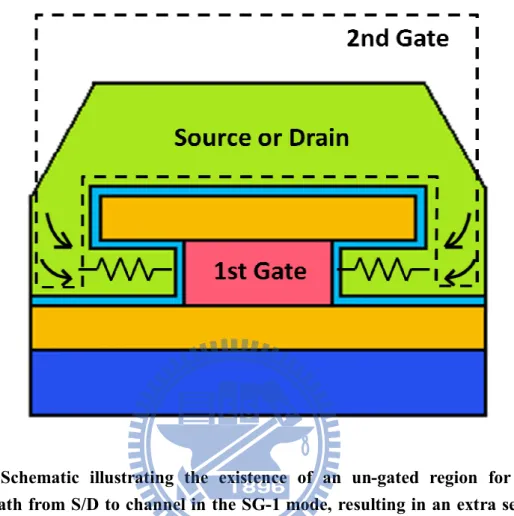
Fig. 3.5. Schematic illustrating the existence of an un-gated region for the current path from S/D to channel in the SG-1 mode, resulting in an extra series resistance. ………. 42 Fig. 3.6. Output characteristics for both devices in the DG mode for (a) 2m
channel length and (b) 0.7m channel length. ………. 43 Fig. 3.7. Total resistance as a function of channel length for (a) IM device and
(b) AcM device. ………. 44 Fig. 3.8. Channel resistance (RTOT-RS/D) as a function of channel length for
both devices. ……… 45 Fig. 3.9. Simulation results of (a) electrical potential and (b) hole density along
channel depth with varying gate overdrive for the IM device. ……….. 46 Fig. 3.10. Simulation results of (a) electrical potential and (b) hole density along
ix
channel depth with varying gate overdrive for the AcM device. ……... 47 Fig. 3.11. SS characteristics of the three operation modes for (a) IM and (b)
AcM devices. ……… 48 Fig. 3.12. Threshold voltage as a function of channel length for the two types of
devices. ……… 49 Fig. 3.13. Location of the conductive channel layer(s) inside the IM and AcM
devices under DG mode of operation. Unlike the IM devices, the current is mainly conducted through the central Si channel and the surface depletion regions result in an additional gate dielectric for the AcM devices. ……… 49 Fig. 3.14. Simulation results of hole density along channel depth with varying
gate overdrive for the AcM device. ……… 50 Fig. 3.15. Schematic illustrating that the EOT for the AcM devices will change
with varying gate bias, which would affect the thicknesses of the depletion regions and the central conductive layer. ……… 50 Fig. 3.16. A simple calculation and definition for the thickness of the additional
gate dielectric of the surface depletion region. ……… 51 Fig. 3.17. EOT of the additional gate dielectric as a function of the gate bias. … 51 Fig. 3.18. SS characteristics of the three operation modes for the (a) IM and (b)
AcM devices with L = 1m. ………. 52 Fig. 3.19. Simulation results of (a) threshold voltage and (b) subthreshold swing
as a function of channel thickness and the channel doping concentration for IM and AcM devices. ………. 53 Fig. 3.20. Simulation results of hole density along channel depth with varying
(a) channel thickness and (b) channel doping concentration for the AcM devices. ………. 54 Fig. 3.21. Illustration of the conductive channel and depletion regions of AcM
devices at Vg=Vth under SG mode with a positive or negative
back-gate bias. Since the drain current is constant as Vg=Vth,
thickness of the conductive channel is roughly a constant, so does the sum of thickness of the two (front- and back-side) depletion regions. . 55 Fig. 3.22. (a) SS-vs.-Vth and (b) distribution of SS measured from 20 AcM
x
Fig. 3.23. (a) SS-vs.-Vth and (b) distribution of SS measured from 20 IM devices under SG-2 mode with varying 1st gate bias. ………. 57 Fig. 3.24. Simulated Vth as a function of channel thickness and back-gate bias
for AcM devices. ……… 58 Fig. 3.25. Ratio of transconductance (Gm) under DG mode to the sum of Gm of
two SG modes for the two types of devices. ………. 58 Fig. 3.26. Potential barrier height as a function of gate overdrive under the
three operation modes for the (a) IM device and (b) AcM device. For the AcM device, the barrier height for DG mode is not only lower than those for SG modes but also decreases more quickly with increasing gate overdrive. ………. 59 Fig. 3.27. Simulation results of electrical potential along the channel depth
under DG and SG modes with the same gate overdrive of 1V for the AcM device. ……….. 60 Fig. 3.28. Simulation results of hole density along channel depth under DG and
SG modes with the same gate overdrive of 1V for the AcM device. ….. 60 Fig. 3.29. Gm ratio for the AcM devices with different channel lengths. As the
channel length gets smaller, the peak value gradually becomes larger. ……….. 61 Fig. 3.30. Simulated electric field along channel depth with varying gate
overdrive for (a) IM device and (b) AcM device. ……….. 62 Fig. 3.31. Normalized transconductance Gm/Gmmax as a function of gate
overdrive for the two types of devices. The Gm degradation in high
- 1 -
Chapter 1
Introduction
1.1 Overview of Multiple-Gated and Poly-Si
Nanowires Transistors
Since the invention of the first transistor by John Bardeen and Walter Brattain in 1947, the revolution of semiconductor industry had spread up like a raging fire. The related applications have advanced the science and technology enormously and improved human’s life in the same time. In order to achieve better electrical performance, many engineers strove to scale down the semiconductor device. They tried to increase the amount of transistors on a chip, expecting to enhance the electrical performance and reduce the cost of the integrated circuits. According to Moore’s Law, the number of transistor on a chip doubles every 18 months. In the early stage of development which roughly followed the constant electric-field (CEF) scaling rules [1], the device scaling could smoothly follow the Moore’s Law without facing too many fatal problems. Unfortunately, when devices scaled dimensions were approaching their physical limitations, many critical problems began to appear, such as short channel effect (SCE) [2], gate leakage current [3] and discrete dopants fluctuation [4], etc. As a result, new materials and/or modifications in device structure came into play in order to extend the Moore’s law.
Recently, as device became increasingly difficult to scale down on account of these problems, many different types of device structure were constantly being
- 2 -
proposed, like multiple-gated field effect transistor (MuG-FET) [5]. These schemes can effectively reduce the impacts of bulk leakage encountered in planar devices, and is thus helpful in improving the control over the SCE. The concept of MuG-FET is extended to lots of novel device structures. A recent typical example is FINFET, which is basically a kind of double-gated device with a fin-like structure. While the planar silicon-on-insulator (SOI) [6] device is considered as a potential device structure in the future, these novel non-planar devices are also receiving considerable attentions in semiconductor industry.
In the meantime, many researches on poly-Si nanowire (NW) channel were invested [7-8]. NW is a one-dimensional structure with its cross-sectional feature size smaller than 100nm. As a result, the NW channel could confine the carriers and enhance their mobility due to its large surface-to-volume ratio. Although it is well known that the defects contained in the granular poly-Si films would aggravate the device characteristics, the adoption of NW structures could help alleviate the effects. Nowadays, the applications of poly-Si NW on thin film transistor (TFT) are seriously considered as an important topic for the future development of semiconductor industry.
For the past several years, more and more researches on the multiple-gate and poly-Si NWs have been presented. There have been many works reported on the fabrication and characterization of devices combining the multiple-gate and poly-Si NW channel [9], and the electrical performance not far behind that of planar CMOS was demonstrated. Due to the convenient and low-cost fabrication process, the devices are appealing for a number of applications like memory [10] and sensor [11].
- 3 -
1.2 Overview of Accumulation-Mode Devices
In essence, the operation principle of the accumulation-mode (AcM) device is similar to the junction field-effect transistor (JFET) [12-13] and the buried-channel MOS device [14-15]. All of them involve the body (or bulk) conduction mechanism, and the current path in the body is modulated by the depletion width controlled by the gate. For the JFET, it can solve the problem from the oxide-semiconductor interface, like the interface traps or the surface roughness scattering. However, the problem for JFET is that the gate-bias range is limited, because the junctions can’t be biased beyond the flat-band voltage (Vfb), otherwise a high leakage current will flow to gate [16]. For theburied-channel MOS device, the surface doping can be of the type opposite to that of the bulk substrate doping. However, this type of device suffers from more severe SCEs than the surface-channel type, thus putting a serious hurdle in device scaling.
For the AcM device, unlike the inversion-mode (IM) device, the source/drain (S/D) and the channel are of the same doping type. To avoid excess bulk leakage current, such type of devices is mainly realized with SOI structure [17]. The operation mechanism of the AcM devices is quite different from that of the IM ones. With a sufficiently thin SOI, the body can be completely depleted by the applied gate bias to avoid the drain-to-source leakage current when device is turned off. With the shrinking of depletion width by decreasing the gate voltage (for p-channel), the cross-sectional area through which holes flow will continue to increase until the depletion regions vanish. For the AcM device, when it is turned on, the current conduction occurs through the whole channel layer rather than the surface. The body current density in the whole channel
- 4 -
region can be expressed as
= , (Eq. 1-1) where n is the average carrier concentration, μb is the effective carrier mobility,
and E is the horizontal electric field. When the total body region is conducting, the cross-sectional area through which holes flow can be expressed as the total body cross-sectional area. By assuming the carrier concentration as the doping concentration and the horizontal electric field as the drain voltage divided by channel length, according to the model of the AcM device in [18], we can further derive the body current as
= = = , (Eq. 1-2) where Na is the doping concentration, tSi is the channel thickness and Vd is the
drain voltage. For the body current, the whole channel acts just like an electrical resistance in relation to the doping concentration, the carrier effective mobility in the bulk and the device dimension. While continuing to reduce the gate voltage, the accumulation charges will be gradually induced and the current conduction on the surface will be added to the drain current. In the same time, the body current will tend to saturate and become independent of the gate voltage, which is also referred in [18].
For the AcM device, the most crucial issue is whether the device can be successfully turned off to evade the large drain-to-source leakage current. In this regard, the gate controllability should be enhanced by thinning the gate dielectric, or the channel thickness should be thin enough for the gate to effectively deplete the carriers. In the past, the relevant technology was not mature and hard to control precisely. The most effective method is to lower the doping concentration in the channel [19], in order to deplete the carriers easily
- 5 -
by the gate bias. In conclusion, on account of the many technical concerns, although several researches had dedicated to the AcM device, such as the analytical model [20] or the extraction method for threshold voltage [21], it was still rarely applied to the planar devices, except for the SOI devices. Recently, due to the rising of the non-planar devices with enhanced gate controllability on channel, many related researches on the AcM non-planar device have been presented, and more and more studies are devoted to this application [22].
1.3 Motivation
For non-planar devices like FinFET, it is becoming more difficult to achieve uniform S/D doping by using implantation on account of shadowing effects caused by tightened pitch with each technology node [23]. Meanwhile, S/D regions for the cell device contained in a high-density 3D memory technology such as BiCS [24] are formed by gate fringing fields from neighboring cells, which are hard to manipulate and may easily result in degradation of read current. In line with this, recently much attention has been paid to the device without junction [25]. In other words, S/D and channel have the same type of doping and the device operates in the AcM.
Our group previously introduced a poly-Si NW transistor with rectangular-shaped NW channels and two independent gates [26]. The two independently controllable gates allow higher flexibility in device operation and provide a unique insight into the conduction mechanism of the NW device. More than this, when the channel thickness is thin enough, the gate-coupling effect with the double gates could occur and enhance the gate controllability on the channel, improving the electrical characteristics like on-current and
- 6 -
subthreshold swing (SS) [27]. Because of these advantages, we tried to apply the double-gated configuration to the AcM device. In this study, we fabricated the p-type AcM double-gated device with a high doping concentration in the channel, expecting to obtain better electrical characteristics via the effective controllability by the double gates. A comparison in device characteristics between the devices with the conventional ones with undoped channels is also made in this study.
1.4 Organization of the Thesis
In Chapter 2, we present the fabrication of the p-type AcM double-gate TFT, and the basic process flow will be briefly described. The measurement setups are also presented in this chapter.
In Chapter 3, we present and discuss the electrical characteristics of the fabricated devices, which include the on-current, SS and SCE. The results of the two single-gated (SG) modes and the double-gated (DG) mode will be discussed respectively. Also, we compare the electrical characteristics with the conventional device.
Finally, we summarize the conclusion from our experimental results and suggest future work in Chapter 4.
- 7 -
Chapter 2
Device Fabrication and Measurement
Setup
2.1 Device Fabrication and Process Flow
In this section, we introduce the basic process flow of the p-type AcM double-gated device. Figure 2.1 shows the schematic process flow of the proposed device. First, a 60 nm-thick SiN layer was deposited on a Si wafer capped with a 100 nm-thick thermal oxide. Because of the p-type doping of the channels, the AcM device prefers a gate material with a low work function such as n+ polycrystalline silicon in order to achieve a suitable threshold voltage (Vth) (that
is, not too positive for p-type device). Therefore, a 100 nm-thick in-situ doped n+ poly-Si and 50 nm-thick SiN were deposited sequentially to serve as the 1st gate stack. After the gate stack patterning (Fig. 2.1(a)), a plasma etching with high selectivity to SiN was used for lateral etching of the n+ poly-Si (Fig. 2.1(b)). Then 10 nm-thick TEOS oxide and 100 nm-thick amorphous Si were deposited, which subsequently underwent 600oC annealing in N2 ambient for 24 hours (Fig. 2.1(c)).
After P+ doping using BF2+ at a dose of 5 × 1014 cm-2 (Fig. 2.1(d)), samples were
annealed in nitrogen ambient at 900oC for 30 min to drive the dopants into the NW channels (Fig. 2.1(e)). To avoid large S/D resistance, an additional S/D doping was performed by implanting BF2+ at a dose of 5 × 1015 cm-2 (Fig. 2.1(f)).
Next, the channel and S/D regions were defined by reactive plasma etching (Fig. 2.1(g)). The 2nd gate electrode comprising of 10 nm-thick TEOS oxide and 100
- 8 -
nm-thick in-situ doped n+ poly-Si was then deposited followed by patterning (Fig. 2.1(h)). A 200 nm-thick oxide was subsequently deposited as passivation layer. The device was completed after standard metallization steps. For the IM device with undoped channels, the fabrication flow is similar to what was described above except that steps in Fig. 2.1(d) and Fig. 2.1(e) are omitted.
The layout of the double-gated device is shown in Fig. 2.2(a). Fig. 2.2(b) is a cross-sectional view of the device along line in Fig. 2.2(a). It can be seen that the 1st gate is surrounded by the SiN layers and two rectangular NW channels.
2.2 Images of Fabricated Devices
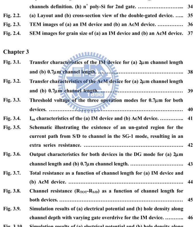
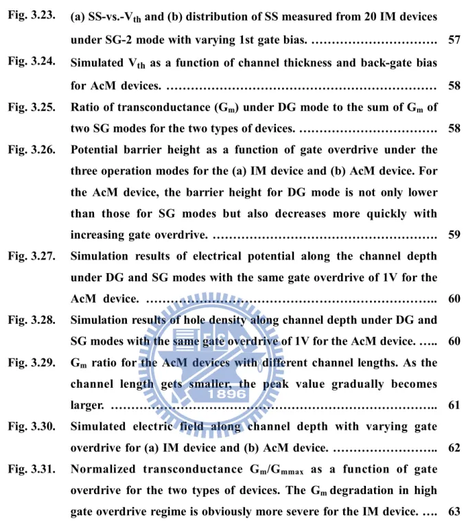
In Chapter 3 we will discuss the electrical characteristics of the fabricated devices including the AcM and the IM devices. However, for the AcM device, its fabrication contained additional channel implant and drive-in steps for driving the dopants into the NW channels, as shown in Fig. 2.1(d) and Fig. 2.1(e). Hence it is imperative to check the texture and grain size of the fabricated NW channels to see if there exists any physical difference between the two devices. Such information is useful for us to compare their electrical characteristics more objectively.
The cross-sectional transmission electron microscope (TEM) images for the fabricated devices are given in Fig. 2.3, from which the rectangular NW channels can be observed. It can be seen that the channel thickness is about 20nm for the IM device and 23nm for the AcM device. From these TEM images, it can be seen that the channel thicknesses for the two devices are roughly the same, though a little thicker for the AcM device.
- 9 -
size in NW channels may become larger. However, prior to the above steps, the AcM device had undergone a 600oC annealing in N2 ambient for 24 hours to
transform the amorphous Si into polycrystalline state, and the grain size for the AcM device may not increase dramatically. This is conformed with the scanning electron microscope (SEM) images of the two types of poly-Si films shown in Figs. 2.4(a) and (b). As can be seen in the figures, the grain sizes for the poly-Si films are similar. Actually the grain size for the AcM device is even slightly smaller than that for the IM device. This phenomenon may be due to the diffusion of high doping concentration of BF2+ [28]. In conclusion, we can approximately
regard the grain sizes for both devices as the same.
2.3 Measurement Setup
In our study, electrical measurements of all devices were evaluated by an HP4156A precision semiconductor parameter analyzer, and the measurement temperature was maintained at 25oC.
The basic electrical parameters of the fabricated device were extracted from the electrical characteristics. By the way, the Vth was not extrapolated from the
Id-Vg curves. Due to the contribution of body conduction for the AcM device, its
operation is different from that of the IM device and the extrapolation technique could be inaccurate [29]. Instead, it is suitable to define the Vth for a fixed drain
current level. The surface potential (ΦS) criterion can be set to zero for the AcM
device [30]. For our experiment, the Vth was defined as the value of Vg when Id
equals 10nA × under Vd of 0.5V, where W and L are the channel width and
the channel length, respectively. For the channel width W, the value was estimated from the TEM images shown in Figs. 2.3(a) and (b) for the IM and
- 10 -
AcM devices, respectively. The SS is calculated by the following equation:
= ( ) , (Eq. 2-1) and for both AcM and IM devices, the minimum value in the subthreshold swing is extracted. The transconductance (Gm) was also extracted from the Id-Vg curves,
and for on-current (Ion), the value was defined as the Id when Vg–Vth = -3V.
For our double-gated structure, the operation modes of measurements are described as below: SG-1 and SG-2 modes denote the scheme when the 1st or 2nd gate serves as the driving gate while the other gate electrode is grounded. In DG mode, both gates are connected together to serve as the driving gate.
- 11 -
Chapter 3
Results and Discussion
3.1 Basic Electrical Characteristics
3.1.1 Transfer Curves
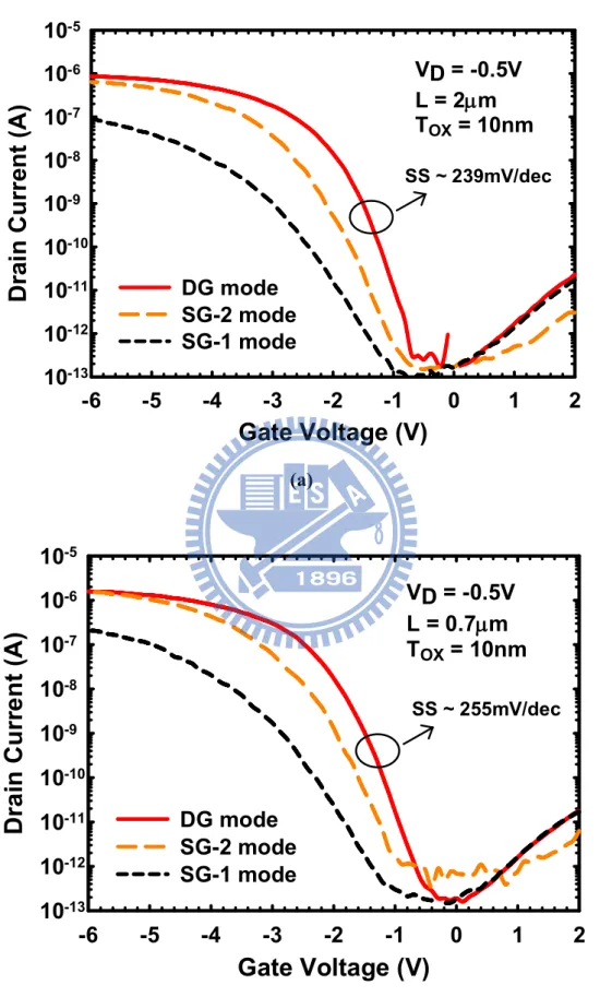
Figure 3.1 shows the transfer curves of an IM device. Due to the existence of un-gated regions which contribute extra parasitic resistances in the SG-1 mode [31], the electrical performance of the SG-1 mode is basically worse than that of the SG-2 mode. For the IM devices, the drain current conducts when the inversion layer is formed near the interface between the channel and gate dielectric. From the plot, we can see the drain currents in the three operation modes rise up at almost the same gate voltage. From the TEM images in Chapter 2, the channel thickness for our fabricated device is quite thin (down to about 20nm), and hence the gate coupling effect [32] is pretty strong so that the gate controllability and electrical performance are obviously enhanced in the DG mode [26]. As is evident in the current-drive of a single device, the Ion of the DG
mode is larger than the sum of those of the two SG modes. Also, owing to the effect of volume-inversion on account of the thin channel thickness [33], the SS under the DG mode is better than that in the SG mode.
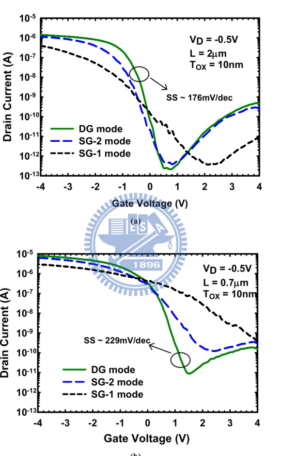
The transfer curves of the AcM device are given in Fig. 3.2. There are some differences in electrical characteristics from those of the IM device. First, it can be seen that the curves of the AcM device apparently shift to the right (more positive value of Vth), showing the normally-on characteristics. Moreover, due to
- 12 -
the different conduction mechanisms for the AcM devices [34], the characteristics of Id-Vg curves are different from those of the IM devices. In the
AcM case, the key point is whether the device can be effectively turned off. When the AcM device is turned on, the channel flowed through by the carriers contained in the accumulation region at the surface and the quasi-neutral region in the film center. On the other hand, for the PMOS devices, if the gate bias isn’t sufficiently positive to deplete the free holes in the channel, a high leakage current will flow and the device cannot be effectively turned off. Thanks to the ultra-thin channel thickness in our fabricated devices, the AcM device can still be successfully turned off in all operation modes despite the very high channel doping (>1018/cm-3). Moreover, for the 0.7µm channel length, the drain-to-source leakage current in each operation modes is significantly larger than that for the device with 2µm channel length. It may be due the severe SCE and the large bulk leakage current for the AcM devices, which will be discussed in the next section. For the AcM devices, the gate coupling effect is also obvious under the DG mode. However, its influence is quite different from that of the IM device. For the DG mode, the two gates are simultaneously used to deplete the channel and can therefore more effectively turn off the device, leading to a smaller SS and a smaller Vth.
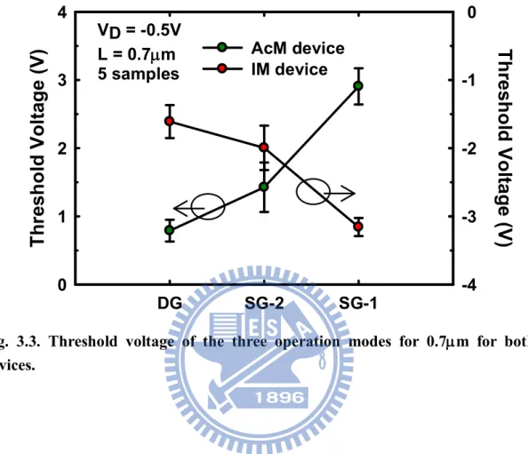
Figure 3.3 shows the threshold voltage (Vth) of the three operation modes for
the two types of devices with 0.7µm channel length. For the IM devices, the conduction is through inversion carriers induced near the channel interface by the gate bias. The Vth is more positive for the DG mode than the SG-2 mode and
SG-1 mode, indicating the IM device can be more effectively switched with the switching mode [27]. However, for the AcM device, the device is normally on and its switching depends on the ability of depleting the carriers in the body. As
- 13 -
shown in Fig. 3.3, the order in the magnitude of Vth among various modes for the
AcM device is opposite to that of the IM one, and the Vth of the DG mode, which
has the strongest gate controllability over the channel, is the smallest. This is reasonable since the DG mode depletes the channel from the two opposite channel interfaces and the two depletion regions would merge at around the center of the channel as the device is turned off. For the SG modes, the depletion starts from only one of the two channel interfaces where the driving bias is applied and it needs to deplete the whole channel for effectively switching off the device, thus the SS is worse while the Vth is larger.
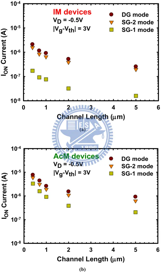
Figure 3.4 shows the Ion characteristics as a function of channel length for
both devices. In the AcM devices, the carriers flow through the whole channel, thus their current level is significantly larger than that of the IM ones in which the conduction is mainly through the channel interface. For the two types of devices, the current of SG-1 mode is smaller than that of SG-2 mode. As explained in [31], the current path of the SG-1 mode contains un-gated regions, as shown in Fig. 3.5, which drastically increase the series resistance. Regarding this problem which leads to the degraded performance, the Ion of the SG-1 mode
is obviously lower than that of the SG-2 mode for the IM devices, and under the DG mode, the Ion is almost dominated by that of the SG-2 mode. This issue is
slightly ameliorated when adopting the AcM scheme, and due to the high doping concentration in the channel, impact of the un-gated regions is relieved, as evidenced by the smaller difference in Ion between the two SG modes.
3.1.2 Output Characteristics
Figure 3.6 shows the output characteristics for both devices. For the AcM devices, the current conduction occurs through the whole channel layer rather
- 14 -
than the surface, and it is apparent that the output current is enhanced significantly for the AcM devices, which can provide about 328% enhancement of saturation current at Vg-Vth = -4V and VD = -5V for the 2µm channel length,
and 198% enhancement for the 0.7µm channel length over the IM devices.
The S/D resistance can be extracted from the Id-Vg curves in Fig. 3.6 by
using the linear regression method. Fig. 3.7 shows the total resistance (Rtot, = )
as a function of channel length. The S/D resistance can be extracted from the intercept of y-axis of the plots. Because we had performed an extra implantation on the AcM devices to reduce the S/D resistance [35], the extracted S/D resistances are almost the same for the two devices. The value of the AcM devices is about 12.4kΩ, just a little smaller than 13.8kΩ of the IM devices, presumably due to the lower-resistivity path in the AcM device between the channel and the S/D as explained in [36]. The channel resistance can be obtained by extracting the S/D resistance from the Rtot, and the results for both devices are shown in Fig.
3.8. Due to the high channel doping for the AcM devices, the channel resistance is much smaller than that for the IM devices with undoped channel. For the long channel length, the difference of channel resistance between the two devices is more obvious, and the difference diminishes with decreasing channel length. The outcome is consistent with the results shown in Fig. 3.6 that the enhancement of the output characteristics is more prominent for the long-channel device.
3.1.3 Simulation Results
Here we use the TCAD simulation to analyze the differences in conduction mechanisms between the two types of devices in the subthreshold region. The simulated structures have a uniform doping concentration in the channel and S/D regions for the AcM devices. The channel has boron doping at a
- 15 -
concentration of 5 × 1018 cm-3, and the channel thickness is 20nm while the gate oxide thickness is 10nm. The work function of gate electrode is 4.15eV, and here we ignore the quantum effect to simplify the condition. The Vth is defined as the
value of Vg when Id equals 10nA. Figure 3.9 shows the simulation results along
the channel depth for the IM devices. As the absolute value of gate overdrive increases in Fig 3.9(a), the energy bands near the interfaces gradually bend and invert the surface region. Then we can see from Fig. 3.9(b) that the concentration of the inverted holes induced near the two interfaces increases with increasing gate overdrive.
The simulation results for the AcM device are shown in Fig. 3.10. In Fig 3.10(a), when the absolute value of gate overdrive increases, the surface bend bending is relieved while the width of a flat-band region (zero electric field) in the central Si channel increases with increasing gate overdrive. It can be noted from Fig. 3.10(b) that the carriers are concentrated at the center of the Si bulk [37]. Unlike the IM device whose channel body is nearly depleted when the device is turned on, the quasi-neutral region of the AcM device gradually expands from the channel center to the interfaces with increasing gate overdrive. In conclusion, from the simulation results, we can define the differences of conduction mechanisms between the two devices. For the IM devices, the conduction carriers are from the surface charges induced by the gate bias, and for the AcM devices with doped channel, the conduction is mainly through the center of the Si bulk opened by the gate bias.
3.2 Subthreshold Characteristics
- 16 -
The SS characteristics as a function of channel length for both devices are given in Fig. 3.11. For the AcM devices, both SG modes start to exhibit obvious rise in SS when the channel length is smaller than 1m. Such phenomenon is relaxed with the DG mode, indicating it has the highest immunity to SCEs among the three modes. Moreover, it is interesting to note that when the channel length is larger than 1m, the SS in the DG mode for the AcM devices is better than that for the IM ones. However, the overall SS degradation with decreasing channel length is still more severe for the AcM devices. The Vth as a function of
channel length is given in Fig. 3.12. It can be seen that the values of Vth for the
AcM devices are all positive, exhibiting the feature of normally-on transistor. However, for the AcM devices, the Vth roll-off is still more severe, and, with
channel length of 0.4m, Vth as high as 2.3V is recorded.
As mentioned above, both SS degradation and Vth roll-off are severer for
the AcM devices, which seem to have worse SCEs than the IM devices, and such phenomenon can be explained from the perspective of the difference in effective oxide thickness (EOT) between the two types of devices. Fig. 3.13 is the schematic illustration of current paths under DG mode of operation for the two types of devices. For the IM devices, the current is mainly conducted along the inversion layer induced near the interfaces and the EOT is approximately equal to the physical oxide thickness. However, for the AcM devices, because the current path in the subthreshold region is mainly along the central Si channel, the physical distance between the gate and the channel is larger than the case of the IM. In other words, there is an additional gate dielectric contributed by the Si depletion layer, resulting in an increase in the EOT of the devices. Moreover, this additional gate dielectric layer not only exhibits in the AcM devices, but also depends on the gate bias. Here we use the TCAD simulation to explain such
- 17 -
situation for the AcM devices with the simulated structures described in the last section, and we use the SG mode to demonstrate in the following simulation.
Figure 3.14 shows the simulation results of the hole density along the channel depth with varying gate overdrive for the AcM device. Gate overdrive conditions used in the simulation for the PMOS device is when the device is turned on, or when the gate voltage is more negative than the Vth. It is seen that
the peak of carrier concentration is moving toward the interface with increasing gate overdrive. Figure 3.15 demonstrates such a trend that the EOT for the AcM devices will change with varying gate bias. Here we define the thickness of the surface Si depletion layer as the average location of the holes with respective to the channel surface, as shown in Fig. 3.16, which can be calculated with the formula given in the figure. We can then quantitatively acquire the contribution of the Si depletion layer to the EOT with the results shown in Fig. 3.17. It can be seen that the additional EOT contributed by the depleted Si channel increases with increasing gate bias. (Note: for PMOS, the increase in gate voltage means the device is turning off). Moreover, the value saturates at around 3.8 nm as the Vg-Vth reaches 2.4V. As a result, for the AcM devices, the EOT is strongly
dependent on the gate bias condition and gradually increases when the device is turned off, explaining the worse SCEs as compared with the IM ones. Such situation can be improved with the DG mode of operation in which the depletion of the channel originating from the two opposite channel surfaces and the EOT contributed by the Si depletion layer can be reduced. This is evidenced with the SS improvement and less SS degradation of the DG mode over the SG modes in Fig. 3.11(b), which is more significant than the effects DG-mode makes for the IM ones shown in Fig. 3.11(a). .
- 18 -
EOT, but the DG mode is still strongly immune to it in terms of the substantially better performance over the SG modes, especially for the short-channel devices.
3.2.2 Variation of Electrical Parameters
Figure 3.18 shows the SS characteristics of the two types of devices under the three operation modes. The results were measured from 10 devices with channel length of 1m. First, for the AcM devices, the SS fluctuation of the SG modes is quite large while the DG mode exhibits relatively smaller one. In contrast with this observation, the IM devices exhibit much smaller SS fluctuation for all operation modes.
Here we also perform simulation to analyze and discuss such a phenomenon. Figures 3.19(a) and (b) show the simulation results of the Vth and SS, respectively,
as a function of channel thickness for both IM and AcM devices operated in the SG mode. It can be seen that, for the AcM devices, the electrical parameters are more sensitive to the channel thickness or the channel doping concentration than those for the IM devices. Actually, such phenomenon has been reported in previous researches [38-39]. According to [39], since the built-in potential between the S/D and channel is lower for the AcM devices than for the IM ones, depletion of the carriers in the center region by the gate biasing is necessary in order to shut the off-state leakage current. However, the higher channel doping concentration gives the shorter depletion width, which results in lower gate controllability at the center of the channel. As a result, the gate controllability is more sensitive to the channel thickness for the AcM devices, and also to the channel doping concentration which will affect the depletion width.
Here we can find out the root cause of such a phenomenon more quantitatively. For the IM devices, the relationship between Vth, channel
- 19 -
thickness and channel doping concentration is analytically given by [40]
= ∙ ∙ , (Eq. 3-1) where Nbody is the channel doping concentration, TSi is the channel thickness, and
Cox is the oxide capacitance. From this equation, a larger fluctuation can be
expected for the AcM devices which have much higher channel doping and thicker EOT. Figures 3.20(a) and (b) show the simulation results of the hole density along the channel depth at Vg=Vth for devices with different channel
thicknesses and channel doping concentrations, respectively. It is obvious that the Si depletion layer between the conductive channel and the gate oxide of the driving gate is becoming larger with increasing channel thickness or the channel doping concentrations, which results in a larger EOT and smaller Cox for the
AcM devices. Such trends would worsen the fluctuation issues and well explain the above experimental results.
Back to the plot of Fig. 3.18(b), for the AcM devices operated under the DG mode, the two gates only need to control a half of the channel thickness which is much thinner as compared to that in the SG mode. The EOT turns out to be thinner and thus the high SS fluctuation described above for the SG mode can be reduced with the DG mode. Convincing data are given in Figs. 3.18(a) and (b).
Based on the above results and analysis we can also infer that the bias condition applied to the back gate may also affect the device characteristics. We can use the schemes shown in Fig. 3.21 to help understand the consequence. In this figure, the two depletion regions, i.e., front (driving)-gate and back-gate sides, in devices operated under the SG mode at Vg=Vth with different bias
applied to the back gate are illustrated. Since Vth is defined as the gate voltage
- 20 -
the channel should be roughly a constant. This means that the back-gate bias may also affect the thickness of channel depletion region of the driving-gate side. As can be seen in the figure that a more positive back-gate bias tends to widen the channel depletion region of the back-gate side, and thus shrink that of the front-gate side. This will reduce the EOT of the device during operation, and thus a reduction in the fluctuation of device characteristics is expected. Conversely, a more negative back-gate bias will worsen the fluctuation issue. Figure 3.22(a) shows the Vth-vs.-SS characteristics measured from 20 devices
with L= 2m under the SG-2 mode. In the figure, 1st gate serves as the back-gate and three biases, namely. -1.5, 0, and 1,5V, are applied. Figure 3.22(b) shows the distribution of measured SS versus G1 bias. Clearly the above inference is confirmed with the measured results. Such dependence is not obvious for the IM devices with the data shown in Fig. 3.23. Fig. 3.24 shows the simulated Vth of the
AcM devices as a function of channel thickness and back-gate bias under the SG mode. It is seen that the dependence on channel thickness is reduced as the back-gate bias increases (or becomes more positive). This well explains and is consistent with the data shown above.
3.3 Transconductance Characteristics
3.3.1 Gate Coupling Effects
Figure 3.25 shows the ratio of transconductance (Gm) under the DG mode to
the sum of Gm of the two SG modes for the two types of devices. The
phenomenon of gate coupling effects can be observed when the channel thickness is thin enough. There are some differences between the two types of devices, and we’ll discuss its influences respectively.
- 21 -
For the IM devices, in general, mobility enhancement can be observed and is attributed to the gate coupling effect which would lead to the occurrence of volume-inversion [41]. In the weak inversion, when the channel thickness is thin enough, the surface band bending at the two sides of the channel would couple with each other under the DG mode, and the whole Si channel could be totally inverted, which is called the volume-inversion [42]. At this moment, the carrier distribution peaks at the center of the poly-Si film where the primary conductive channel is located. As a result, the current-drive is dominated by these minority carriers, which are less confined at the interfaces and won’t suffer from serious surface roughness scattering and the interface states as compared with the cases of the SG mode [32]. The advantage of such effect is shown in the experimental difference in Gm between the SG mode and DG mode (exceeding a factor of 2),
and this enhancement is primarily related to the increase in carrier mobility. In Fig. 3.25 we can see that, for the IM device, the peak value of Gm ratio is almost
up to 1.5. In the DG mode, as the gate overdrive increases the carrier distribution moves gradually closer to the two interfaces and the situation becomes more like the SG modes. This explains why the Gm ratio is close to unity
with increasing gate overdrive, which is the theoretical value if the gate coupling effect doesn’t exist.
However, for the AcM devices, the influence of the gate coupling effect is different from the IM devices. Specifically, when the AcM device is turned on, most of the Si channel is in quasi-neutral condition. The current-drive is mainly conducted through the whole channel for both SG and DG modes, thus the mobility enhancement mentioned above is not obvious here. Here we extract the values of potential barrier height to confirm such mechanisms. According to the Levinson’s mode based on the thermionic field conduction model [43], the
- 22 -
channel mobility µeff can be divided into the intragrain mobility µG and the
mobility at the grain boundary (qvcLg/kT.exp[-Eb/kT]). Thus the µeff can be
expressed as
= + ( ) , (Eq. 3-2) where vc is the collection velocity, Lg isthe grain size and Eb is the potential
barrier height at the grain boundary [44]. If the intragrain mobility is assumed to be the same as that in single crystal Si bulk and much higher than the mobility at the grain boundary, then µeff can be reduced to
~ ( ) . (Eq. 3-3) When device is turned on, the drain current can be expressed as
= − − ∝ ( ) . (Eq. 3-4) Here we can approximately regard the potential barrier height Eb as the
activation energy of drain current, which can be obtained from the slope of the Arrhenious plot of drain current.
Figure 3.26 shows the potential barrier height as a function of gate overdrive in the three operation modes. The data give some clues for understanding the difference in conduction between the two types of devices. For the IM devices, due to the aforementioned gate coupling effect, the barrier height for the DG mode is lower than those for the SG modes with varying gate overdrive. This is consistent with the superior DG performance in terms of better SS and the larger Ion. However, for the AcM devices, it can be seen that
the barrier height for the DG mode is not only lower than those for the SG modes, but also decreases more quickly with increasing gate overdrive. The greater Gm enhancement for AcM devices shown in Fig. 3.25 can be attributed to
- 23 -
compared with the IM devices. The results of the TCAD simulation for the electrical potential along the channel depth of the AcM device under SG and DG operations with the same gate overdrive of 1V are shown in Fig. 3.27. When the AcM devices are turned on under the DG mode, the two gates simultaneously relieve the surface bend bending while the width of a quasi neutral region in the central Si channel increases with increasing gate overdrive. This means the conductive region in the channel would be wider than that of the SG mode. This is convinced with the results shown in Fig. 3.28 which illustrates the simulated hole concentration under the conditions of Fig. 3.27. It is seen that the carrier density in the DG mode is significantly larger than that in the SG mode with the same gate overdrive, and the significant Gm enhancement of the DG operation is
also attributed to the larger amount of holes.
Another important finding for the AcM devices is that the peak value of Gm
ratio shows dependence on the channel length. Such trend is not obvious for the IM devices. Figure 3.29 shows the Gm ratio with different channel lengths for the
AcM devices. It can be seen that as the channel length is shorter, the peak value becomes larger, e.g., up to 4.6 with channel length of 0.7m. The reason is attributed to the severer SCEs for the AcM devices. As mentioned above, the SG modes exhibit a worse SS degradation which also degrades the Gm. Since the DG
mode shows higher immunity to the SCEs, the Gm difference between the SG
mode and DG mode becomes more prominent with shorter channel length.
3.3.2 Transconductance Degradation
As we mentioned earlier, for the AcM devices, when the device is turned on, most of the channel is basically in quasi-neutral condition. For the IM devices, the carriers in the inversion layer are attracted by the gate bias, resulting in a
- 24 -
severe band bending [45]. The TCAD simulation results are shown in Figs. 3.30(a) and (b) for the IM and AcM devices, respectively. As can be seen in the figures, the electric field at the surfaces is much larger for the IM devices. Besides, for the AcM devices, the much lower gradient of electric field near the central region also indicates that the central bulk is a quasi-neutral region when the device is turned on. The normalized Gm (Gm/Gm.max) as a function of gate overdrive is
given in Fig. 3.31, from which we can see that the Gm degradation in high gate
overdrive regime is more severe for the IM device [46]. For the AcM devices, the conduction is through the whole channel and thus the carriers might inherently suffer less from the scattering of the surface roughness and the interface traps.
- 25 -
Chapter 4
Conclusion and Future Work
4.1 Conclusion
In this work, we have fabricated and characterized a novel p-type AcM double-gated poly-Si NW transistors featuring an independent double-gated configuration. Thanks to the ultra-thin channel thickness of 20nm, the AcM devices can still be turned off under all operation modes, despite a high doping concentration is contained in the channel. Moreover, as compared with the IM counterparts, some intriguing characteristics are revealed. As the AcM devices are on, the carriers flow mainly through the whole channel, thus the current level is significantly larger than that of the IM ones in which the conduction is mainly through the induced inversion layer near the channel interface. From the TCAD simulation results, distribution of the carriers in the channel and the operation mechanisms of the two types of devices are analyzed. Unlike the IM device whose channel body is essentially depleted when the device is turned on, the quasi-neutral region of the AcM device gradually expands from the channel center to the interfaces with increasing gate overdrive.
For the subthreshold characteristics, due to the additional EOT contributed by the surface depletion region, the AcM devices exhibit worse SCEs than the IM devices, resulting in severer SS degradation and Vth roll-off. Moreover, the
variation of electrical parameters is also severer for the AcM devices due to the higher EOT and high channel doping concentration, representing another major
- 26 -
issue for the AcM devices. Fortunately, these problems for the AcM devices would be ameliorated with a thinner channel thickness and DG operation. Our analysis and experimental results pointed out that the bias condition applied to the back gate would also affect the fluctuation in device characteristics.
On the other hand, from the transconductance characteristics and simulation results, for the AcM devices, the influence of the gate coupling effect is different from the IM devices. The greater Gm enhancement with the DG
operation relative to SG modes for the AcM devices can be attributed to the quicker lowing in barrier height and the larger amount of holes as compared with the IM devices. Moreover, the peak value of Gm ratio shows dependence on
the channel length. That’s because the DG mode has higher immunity to the SCEs than the SG mode. Moreover, from the simulation results, the electric field at the surfaces of the IM device is larger than that of the AcM device at the same gate overdrive. For the AcM devices, the conduction is through the whole channel and thus the carriers inherently suffer less from the scattering of the surface roughness and the interface traps, as we can see that the Gm degradation
in high gate overdrive regime is more severe for the IM device.
4.2 Future Work
In this study, we’ve successfully fabricated the p-type AcM double-gated poly-Si NW devices and compared their electrical characteristics with those of the IM devices with undoped channels. One of our initial goals is to perform in-situ doped deposition for preparing the poly-Si films so the device’s S/D and channel have the same doping type and level. But being limited by the available techniques, such goal is not achieved in this work. This topic, however, deserves
- 27 -
future effort to achieve. Besides, effects of the doping concentration in the channel and the channel thickness remain not so clear and should be further investigated in the future.
- 28 -
References
[1] B. Davari, R. H. Dennard, and G. G. Shahidi, “CMOS scaling for high performance and low power-the next ten years,” Proc. IEEE, vol. 83, no. 4, pp. 595–606, Apr. 1995.
[2] B. Yu, C. H. J. Wann, E. D. Nowak, K. Noda, and C. Hu, “Short-channel effect improved by lateral channel-engineering in deep-submicrometer MOSFETs,” IEEE Trans. Electron Devices, vol. 44, no. 4, pp. 627–634, Apr. 1997.
[3] K. Roy, S. Mukhopadhyay, and H. Mahmoodi-Meimand, “Leakage current mechanisms and leakage reduction techniques in deep-submicrometer CMOS circuits,” Proc. IEEE, vol. 91, no. 2, pp. 305–327, Feb. 2003.
[4] Y. Taur, H. S.Wong, and D. J. Frank, “Discrete random dopant distribution effects in nanometer scale MOSFETs,” Microelectron. Reliab., vol. 38, no. 9, pp. 1447–1456, Sep. 1998.
[5] J. T. Park and J. P. Colinge, “Multiple-gate SOI MOSFETs device design guidelines,” IEEE Trans. Electron Devices, vol. 49, no. 12, pp.2222-2229, Dec. 2002.
[6] W. Baerg, J.C. Sturm, T. L. Hwa, H. Y. Lin, B. B. Siu, C. H. Ting, J. C. Tzeng and J. F. Gibbons, “A seeded-channel silicon-on-insulator (SOI) MOS technology,” IEEE Electron Device Lett., vol. 6, no. 12, pp. 668–670, Dec. 1985.
[7] H. C. Lin, M. H. Lee, C. J. Su, T. Y. Huang, C. C. Lee, and Y. S. Yang, “A simple and low-cost method to fabrication TFTs with poly-Si nanowire channel,” IEEE Electron Device Lett., vol. 26, no. 9, pp. 643–645, Sep. 2005. [8] K. W. Kolasinski, “Silicon nanostructures from electroless electrochemical