662 IEEE PHOTONICS TECHNOLOGY LETTERS, VOL. 19, NO. 9, MAY 1, 2007
Nearly White-Light Emission From GaN-Based
Light-Emitting Diodes Integrated With a
Porous SiO
2
Layer
Chih-Hao Hsieh, Min-Yung Ke, Ghien-An Shih, Tzu-Yang Chiu, and Jian Jang Huang
Abstract—In this letter, we develop a nearly white-light-emitting device by integrating blue/green emission from a GaN-based light-emitting diode with red emission from a porous SiO2 layer. The porous SiO2layer was fabricated by a novel process procedure to create Si nanocrystals on top of the n-type GaN layer. Red light is generated from the metal–oxide–semiconductor (Ni–Au–SiO2
oxide-n-type GaN) structure due to the electron–hole recombina-tion in the Si nanocrystals. The device shows a blue light emission at a low biased voltage and nearly white-light emission (green and red colors) at a bias voltage between 14 and 16 V. Our results show the potential of applying such an integrated structure to white-light illumination.
Index Terms—Light-emitting diodes (LEDs), Si-nanocrystal, SiO2porous layer, white light.
I. INTRODUCTION
W
HITE-LIGHT-EMITTING diodes (LEDs) have become popular due to their applications to backlights for thin-film transistor-liquid crystal displays and general lighting. Typically, they can be fabricated with the combination of discrete red, green, and blue LEDs [1]. The phosphor converted LED is an alternative approach for white-light illumination [2]. They can be realized by mixing blue light from GaN-based LEDs with yellow light converted from the blue pumped phos-phor, or by mixing green, red, and blue colors converted from ultraviolet pumped phosphors [3]. Despite the availability of choices of using phosphor species for selected wavelength con-version, there are disadvantages of phosphor converted LEDs. For example, the conversion efficiency of phosphor species is typically very low. This poor energy conversion is due to a Stokes energy loss when converting short-wavelength photons to long wavelength ones. Also, the phosphor converted LEDs do not allow for the extensive tunability, particularly in terms of spectral modulation [1]. In light of those drawbacks, direct electron–hole recombination or direct optical pump semicon-ductor materials are alternate candidates for high efficient light sources.Manuscript received June 23, 2006; revised December 13, 2006. This work was supported by the National Science Council, Taiwan, under Grant NSC 94-2215-E-002-028.
The authors are with the Graduate Institute of Electro-Optical Engineering and Department of Electrical Engineering, National Taiwan University, Taipei, 106 Taiwan, R.O.C. (e-mail: [email protected]).
Digital Object Identifier 10.1109/LPT.2007.893760
Silicon nanocrystals (nc-Si) embedded in SiO matrix nc-Si–SiO is attracting a lot of interest in its efficiency and stability of light emission at room temperature. Various technologies have been proposed to fabricate nc-Si structures, such as plasma-enhanced chemical vapor deposition (PECVD) [4], electron-beam evaporation [5], and Si-ion implantation [6]. Photoluminescence (PL) spectra from the blue to near-infrared region were demonstrated [7]–[9]. Even though it is generally thought that the quantum confinement effect is one of the main mechanisms for light emission, point defects, such as from Si-ion-implanted SiO , are also considered to be another source for light emissions [10]. In addition, electroluminescence (EL) spectra of the metal–oxide–semiconductor (MOS) structures (where the material nc-Si–SiO or Si-ion implanted SiO is regarded as the oxide layer and Si substrate as the semicon-ductor) were also reported with turn-on voltages between 3.3 and 86 V in the 700 900 nm wavelength range [10]–[12].
In this letter, we develop a novel integrated white-light-emit-ting device. By combining the nc-Si MOS with the GaN-based LED structure, i.e., by depositing a porous SiO layer on top of the GaN-based LED, nearly white-light emission with dual spectrum peaks at 496.4 and 828.6 nm are demonstrated at room temperature. The turn-on voltage of the nc-Si MOS device is as low as 13.7 V and the operation voltage of the nearly white-light MOS-LED device is between 14 and 16 V. The MOS-LED structure shows the potential of applying such an integrated de-vice to white-light generation.
II. MATERIALGROWTH ANDDEVICEFABRICATION
The GaN-based LED sample with a PL peak at around 480 nm was grown on a c-plane sapphire substrate by metal–or-ganic chemical vapor deposition. The material structure is com-posed of a 25-nm GaN buffer layer, a 1.8- m Si-doped n-type GaN layer, a ten-period InGaN–GaN multiple quantum-well structure, and a 200-nm p-type GaN layer. The patterned SiO layer was deposited on top of the GaN n-type layer by PECVD with an initial thickness of 340 nm. We then wet-etched the SiO layer by buffer oxide etcher (NH F : HF ) to thin down the SiO layer. In the subsequent step, the sample was dry etched by inductively coupled plasma reactive ion etching to create porous profile on SiO layer. We used Ar, SiCl and Cl as etching gases with a flow rate 20, 1, and 15 sccm, respec-tively. The SiO layer thickness was optimized by considering both the generated output optical power from the SiO layer (nc-Si) and the operating voltage. Typically, a thicker SiO layer is preferred for luminescence which, however, requires a
1041-1135/$25.00 © 2007 IEEE
HSIEH et al.: NEARLY WHITE-LIGHT EMISSION FROM GaN-BASED LEDs 663
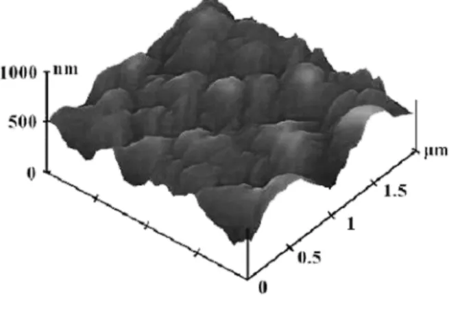
Fig. 1. AFM surface profile of the porous SiO layer.
Fig. 2. Schematic illustration of a GaN-based LED integrated with a porous SiO layer.
higher biased voltage. In our case, the optimum thickness of the porous SiO layer is around 200 nm. The atomic force micro-scopic (AFM) surface profile of the porous SiO layer grown on top of the n-type GaN layer is shown in Fig. 1. The lateral diameter of nc-Si is approximately 500 nm. In the next step, Ni–Au metal layers were evaporated as the p-type electrode and were alloyed to obtain optimized ohmic contact condition. We then coated Ti–Au directly on top of the porous SiO layer as the n-type contact. The Ti–Au–SiO GaN layer combination forms an MOS structure (see Fig. 2) and red emission can be observed after a 750 C annealing in our experiment. The high-temperature annealing ( 700 C) deactivates the neutral oxygen vacancies defect O Si Si O in the porous SiO layer, and meanwhile generates nc-Si [13]. Electron-hole recombination can occur in the porous SiO layer (nc-Si).
III. CHARACTERIZATIONS
The EL spectra of our samples were taken at various bias volt-ages [see Fig. 3(a)] at room temperature. At a low bias voltage, electrons from the n-type electrode tunnel through the porous SiO layer and recombine with holes in the GaN-based active layer to generate blue emission. Therefore, the blue emission is dominated at low bias voltages. The peak wavelength is around 487.6 nm when biased at 14 V. As we increase the applied voltage to 15 V, red emission is observed as the carrier recombi-nation in the MOS structure starts to occur. It is also noted that the relative intensity of the blue emission decreases as the ap-plied voltage increases, which is attributed to the fact that more and more carriers are recombined in the MOS region when the bias voltage increases from 14 to 15 V. The blue emission is fur-ther decreased as the applied voltage is increased to 16 V. The peak wavelength of the GaN-based LED is shifted to 496.4 nm
Fig. 3. (a) Room-temperature EL spectra and (b) CIE 1931 chromaticity dia-gram of the light emission of LEDs at bias voltages 14, 15, and 16 V.
due to quantum confinement stark effect. The relative intensi-ties of wavelength 496.4 and 828.6 nm have become compa-rable at the bias voltage 16 V. Fig. 3(b) shows the CIE 1931 chromaticity diagram with corresponding light-emitting colors at different bias voltages. With the increase of bias voltages, the bluish color ( , ) at 14 V turns to a nearly white color ( , ) at 16 V.
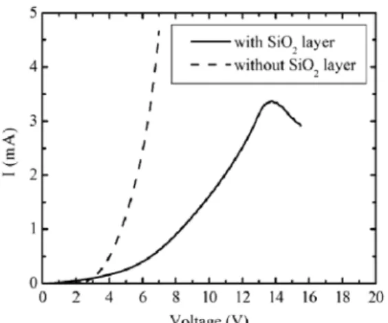
We further compare the current–voltage ( – ) characteristic of the MOS-LED structure with that of the conventional LED sample (the one without any SiO layer coated). As shown in Fig. 4, the – curve of the conventional LED shows a diode be-havior (dashed line), while that of the MOS-LED structure acts like a normal LED in series with a resistor when the bias voltage is below 13.7 V. Since carriers from the n-type electrode of the MOS-LED structure have to tunnel through the thin porous SiO layer, the effective current under the same bias voltage of the MOS-LED structure is smaller than that of the conven-tional LED structure. When the bias voltage is above 13.7 V (the threshold voltage of the MOS device), the device is turned on and electrons from the n-type electrode start to recombine with holes in the nc-Si. A negative resistance is observed at bias voltages above 13.7 V, indicating the generation of red light. The negative resistance in Fig. 4 corresponds to the onset of red light emission in Fig. 3 and meanwhile indicates the decrease
664 IEEE PHOTONICS TECHNOLOGY LETTERS, VOL. 19, NO. 9, MAY 1, 2007
Fig. 4. I–V curves of the MOS-LED sample (solid line) and the conventional LED (dashed line).
of blue intensity. The MOS structure breaks down (blows up) at bias voltages beyond 16 V, which is due to large numbers of electrons tunneling through the porous SiO layer.
IV. CONCLUSION
We have developed a novel integrated white-light-emitting device. By integrating the nc-Si MOS with the GaN-based LED structures, i.e., by depositing a porous SiO layer on top of the GaN-based LED, nearly white-light emission with dual spec-trum peaks at 496.4 and 828.6 nm were demonstrated at room temperature. The turn-on voltage of the nc-Si MOS device is as low as 13.7 V and the operating voltage of the nearly white-light MOS-LED device is between 14 and 16 V. In addition, a nega-tive resistance is observed from the – curve of the MOS-LED structure at a bias voltage above 13.7 V. It is attributed to the fact that some carriers start to recombine in the MOS region. The rel-ative intensity of red emission is thus increased while that of the blue emission is decreased. Our results indicate the potential of applying such an integrated structure to white-light generation.
REFERENCES
[1] E. F. Schubert and J. K. Kim, “Solid-state light sources getting smart,”
Science, vol. 308, no. 5726, pp. 1274–1278, May 27, 2005.
[2] H. Wu, X. Zhang, C. Guo, J. Xu, M. Wu, and Q. Su, “Three-band white light from InGaN-based blue LED chip precoated with green/red phos-phors,” IEEE Photon. Technol. Lett., vol. 17, no. 6, pp. 1160–1162, Jun. 2005.
[3] J. K. Sheu, S. J. Chang, C. H. Kuo, Y. K. Su, L. W. Wu, Y. C. Lin, W. C. Lai, J. M. Tsai, G. C. Chi, and R. K. Wu, “White-light emission from near UV InGaN-GaN LED chip precoated with blue/green/red phosphors,” IEEE Photon. Technol. Lett., vol. 15, no. 1, pp. 18–20, Jan. 2003.
[4] D. Pacifici, E. C. Moreira, G. Franzò, V. Martorino, F. Priolo, and F. Ia-cona, “Defect production and annealing in ion-irradiated Si nanocrys-tals,” Phys. Rev. B, vol. 65, p. 144109, Apr. 2002.
[5] Q.-Y. Ye, R. Tsu, and E. H. Nicollian, “Resonant tunneling via micro-crystalline-silicon quantum confinement,” Phys. Rev. B, vol. 44, no. 4, pp. 1806–1811, 1991.
[6] A. Pèrez-Rodrìguez, O. González-Varona, B. Garrido, P. Pellegrino, J. R. Morante, C. Bonafos, M. Carrada, and A. Claverie, “White lumi-nescence from Si and C ion-implanted SiO films,” J. Appl. Phys., vol. 94, no. 1, pp. 254–262, Jul. 2003.
[7] X. Zhao, O. Schoenfeld, J. Kusano, Y. Aoyagi, and T. Sugano, “Ob-servation of direct transitions in silicon nanocrystallites,” Jpn. J. Appl.
Phys., vol. 33, no. 7A, pt. 2, pp. L899–L901, Jul. 1994.
[8] T. Shimizu-Iwayama, K. Fujita, S. Nakao, K. Saitoh, T. Fujita, and N. Itoh, “Visible photoluminescence in Si -implanted silica glass,” J.
Appl. Phys., vol. 75, no. 12, pp. 7779–7783, Jun. 1994.
[9] P. Mutti, G. Ghislotti, S. Bertoni, L. Bonoldi, G. F. Cerofolini, L. Meda, E. Grilli, and M. Guzzi, “Room-temperature visible lumines-cence from silicon nanocrystals in silicon implanted SiO layers,”
Appl. Phys. Lett., vol. 6, pp. 851–853, Feb. 1995.
[10] G.-R. Lin, C.-J. Lin, C.-K. Lin, L.-J. Chou, and Y.-L. Chueh, “Oxygen defect and Si nanocrystal dependent white-light and near-infrared electroluminescence of Si-implanted and plasma-enhanced chem-ical-vapor deposition-grown Si-rich SiO ,” J. Appl. Phys., vol. 97, pp. 094306–094306-8, Apr. 2005.
[11] G. Franzò, A. Irrera, E. C. Moreira, M. Miritello, F. Iacona, D. Sanfil-ippo, G. Di Stefano, P. G. Fallica, and F. Priolo, “Electroluminescence of silicon nanocrystals in MOS structures,” Appl. Phys. A: Mater. Sci.
Process., vol. 74, no. 1, pp. 1–5, Jan. 2002.
[12] J. Valenta, N. Lalic, and J. Linnros, “Electroluminescence microscopy and spectroscopy of silicon nanocrystals in thin SiO layers,” Opt.
Mater., vol. 17, no. 1–2, pp. 45–50, Jun. 2001.
[13] J. H. Son, T. G. Kim, S. W. Shin, H. B. Kim, W. S. Lee, S. Im, J. H. Song, C. N. Whang, and K. H. Chae, “Blue and red luminescence from Si ion-irradiated SiO /Si/SiO layers,” Opt. Mater., vol. 17, no. 1–2, pp. 125–129, Jun. 2001.