國 立 交 通 大 學
電信工程學系
碩 士 論 文
3–6 GHz 超寬頻低功率自順向基底偏壓
低雜訊放大器設計
3–6 GHz Ultra-Wideband Low-Power
Self-Forward-Body-Bias Low-Noise Amplifier
研 究 生:李振銘
指導教授:唐震寰 教授
3
–
6 GHz 超寬頻低功率自順向基底偏壓低雜訊放大器設計
3
–
6 GHz Ultra-Wideband Low-Power Self-Forward-Body-Bias
Low-Noise Amplifier
研 究 生:李振銘 Student:Chen-Ming Li
指導教授:唐震寰 博士 Advisor:Dr. Jenn-Hwan Tarng
國 立 交 通 大 學
電 信 工 程 學 系 碩 士 班
碩 士 論 文
A Thesis
Submitted to Department of Communication Engineering College of Electrical Engineering and Computer Science
National Chiao Tung University in Partial Fulfillment of the Requirements
for the Degree of Master
in
Communication Engineering
July 2009
Hsinchu, Taiwan, Republic of China
3
–
6-GHz
超寬頻低功率自順向基底偏壓低雜訊放大器設計
研究生:李振銘 指導教授:唐震寰
國立交通大學
電信工程學系 碩士班
摘要
於本論文,我們提出一使用 0.18-µm TSMC CMOS 1P6M 製程應用於超寬頻低頻帶系 統之低功率自順向基底偏壓低雜訊放大器。使用自順向基底偏壓技術,可以降低低雜訊 放大器的供應電壓並且也可以節省額外的偏壓電路,而使我們的低雜訊放大器在兩個汲 極-源極的電壓降之供應電壓為 1.06 V 為低功率消耗。而 LNA 電路裡的互補式架構與第 二級直接耦合的方式也節省了額外所需的偏壓電路。由於提出的自順向基底偏壓技術對 於雜訊指數有些許不好的影響,因此,我們針對此問題將先前提出的低雜訊放大器之雜 訊指數做改善。在本論文的一些圖表中,所提出第一個的低雜訊放大器之量測數據顯示, 在功率消耗 6.38 mW 且頻寬為 2.6 至 6.6 GHz,最大增益為 15.5 dB,輸入/輸出阻抗匹 配之功率反射係數分別為低於-12 dB 及 -17dB,平均雜訊指數為 3.2 dB。而改善後的 低雜訊放大器之量測結果顯示,在功率消耗 4.5 mW 且頻寬為 2.0 至 6.6 GHz 下,最大 增益為 16.2 dB,輸入/輸出阻抗匹配之功率反射係數分別為低於-12 dB 及 -16dB,平 均雜訊指數為 2.6 dB。3–6-GHz Ultra-Wideband Low-Power
Self-Forward-Body-Bias Low-Noise Amplifier
Student:Chen-Ming Li Advisor:Dr. Jenn-Hwan Tarng
Department of Communication Engineering
National Chiao-Tung University
Abstract
A low-power low-noise amplifier (LNA) implemented in 0.18-μm TSMC CMOS 1P6M technology utilizing a self-forward-body-biased (SFBB) technique is proposed for UWB low-frequency band system in this thesis. By using the SFBB techniques, it reduces supply voltage as well as saves additional biased circuits used in conventional FBB techniques, which leads to a low power consumption with low supply voltage of 1.06 V for two MOSFETs drain-to-source voltage drops. Using the complementary configuration and inter-stage direct coupling technique also saves the biased circuits. However, the self forward body bias technique will give rise to some noise figure degradation. Therefore, we proposed the second LNA to improve the noise figure of the preceding LNA in this thesis. The measurement result shows that the LNA 1 also presents a maximum power gain of 15.5 dB with a good input/output match (S11< –12 dB/ S22< -17 dB) and an average noise figure of 3.2
dB in the frequency range of 2.6–6.6 GHz while consuming power of 6.38 mW. And the measurement result shows that the NF-improved LNA presents a maximum power gain of 16.2ddB with a good input/output match (S11< -12 dB/ S22< -16 dB) and an average noise
誌
謝
在碩士班研究的這二年歲月,首先要感謝的是我的指導教授 唐震寰教授並致上我 最誠摯的謝意。感謝老師在專業的通訊領域中,給予我不斷的指導與鼓勵,並賦予了實 驗室豐富的研究資源與環境,使得這篇碩士論文能夠順利完成。同時,亦感謝口試委員 國立臺灣大學 李學智教授及國立臺灣科技大學 楊成發教授對於論文內容所提出的 寶貴建議及指導,在此致上最誠懇的謝意。 其次,要感謝波散射與傳播實驗室的學長們—佩宗學長、清標學長、俊諺學長、雅 仲學長、豐吉學長、奕慶學長、威璁學長、智偉學長、稟文學長、文崇學長、瑞榮學長 等在研究上的幫助與意見,讓我獲益良多。感謝實驗室的同學—明宗、廣琪、兆凱等在 課業及研究上的互相砥礪與切磋,以及生活上的多彩多姿。亦感謝學弟們—冠豪、國政、 鉦浤、耿賢等,讓實驗室在嚴肅的研究氣氛中增添了許多歡樂,有了你們,更加豐富了 我這二年的研究生生活。另外,也要感謝助理—梁麗君小姐,在實驗室上的協助和籌劃 每次的美食聚餐饗宴。 最後,要感謝的就是我最親愛的家人。他們在我求學過程中,一路陪伴著我,給予 我最溫馨的關懷與鼓勵,讓我在人生的過程裡得到快樂,更讓我可以專心於研究工作中 而毫無後顧之憂。 鑒此,謹以此篇論文獻給所有關心我的每一個人。 李振銘 誌予 九十八年七月CONTENTS
ABSTRACT (CHINESE) ………Ⅰ
ABSTRACT (ENGLISH) ………Ⅱ
ACKNOWLEDGEMENT………Ⅲ
CONTENTS………Ⅳ
LIST OF TABLES………Ⅶ
LIST OF FIGURES………Ⅷ
CHAPTER 1 Introduction 1
1.1 Background and Problems………1
1.2 Related Works………2
1.3 Thesis Organization………3
CHAPTER 2 Basic Concepts of Low-Noise Amplifier Design 4
2.1 System Specifications of LNA………4
2.1.1 S-Parameters………4
2.1.2 Noise Figure (NF) ………6
2.1.3 Harmonics………7
2.1.4 1-dB Gain Compression Point (P1dB) ………8
2.1.5 Inter-Modulation………9
2.2 Conventional Wideband Input Impedance Matching Architecture…………11
2.2.1 Resistor Termination Architecture………12
2.2.2 Shunt-Series Resistor Feedback Architecture………13
2.2.3 Common-Gate Architecture (1/gm Termination) ………13
2.2.4 Inductive Source Degeneration with Broadband-Pass Filter…………14
2.2.5 Inductive Source Degeneration with Transformer………16
2.2.6 Distributed Amplifier………17
2.2.7 Comparison of Wideband Input Matching Architectures………17
2.3 Methods to Reduce Noise Figure of LNA………19
2.3.1 Gain-Driven Overlap Capacitance Neutralization Method………19
2.3.2 Miller Effect Mitigation Method by Using Cascode Configuration…20 2.3.3 Feed-Forward Thermal Noise Canceling Method………20
2.3.4 Input-Matching Device Thermal Noise Reduction Method by Using Mutual Inductor………21
2.3.5 Quality Factor (Q) of Inductor Enhancement Method………22
2.4 Considerations of LNA Design………24
CHAPTER 3 Review of Low-Power LNA Design 25
3.1 Introduction………25
3.2 Current-Reused Technique………26
3.3 Common-Gate Configuration with Non-50-Ω Input Impedance Technique…27 3.4 Gain Boost by Using Mutual Inductor Technique………28
3.5 Forward Body Bias Technique………29
3.6 Dynamic-Threshold Voltage Technique………30
CHAPTER 4 Design of Low-Power Self Forward Body Bias UWB LNA 32
4.1 Introduction………32
4.2 The Proposed Low-Power UWB LNA………33
4.2.1 Design of Input/Output Impedance Matching………33
4.2.2 Gain Bandwidth Extension………36
4.2.3 Self Forward Body Bias (SFBB) Technique………37
4.2.4 Noise Analysis of The Proposed LNA………42
4.2.5 Layout Consideration………45
4.2.6 Simulation and Measurement Result………46
4.3 Noise Improvement for The Preceding Low-Power SFBB UWB LNA………56
4.3.1 Noise Improvement for SFBB Technique………56
4.3.2 Measurement Result………59
CHAPTER 5 Conclusion 65
List of Tables
Table 2.1 Comparison of wideband input matching architectures………17 Table 3.1 Comparison of low-power consumption techniques………31 Table 4.1 Simulated performance summary of wi/wo SFBB for different supply
voltage………51 Table 4.2 The performance summary of the proposed LNA and comparison with several papers………55 Table 4.3 The performance summary of the noise-improved LNA and comparison with several papers………64
List of Figures
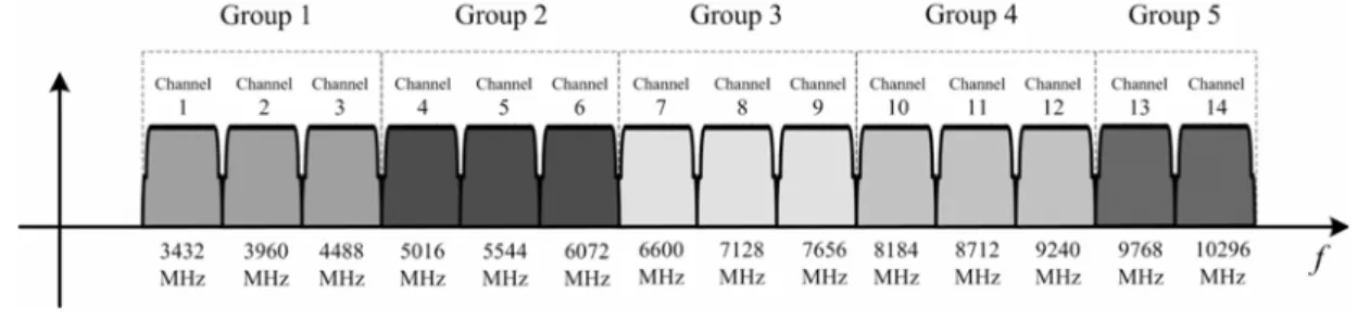
Figure 1.1 UWB Multi-Band OFDM Proposal………1
Figure 2.1 Two-port network with S-parameters………5
Figure 2.2 Cascade of system block diagram………6
Figure 2.3 Frequency response of nonlinear system with one tone signal………7
Figure 2.4 Definition of 1-dB compression point………8
Figure 2.5 Inter-modulation in LNA (nonlinear system) ………9
Figure 2.6 The input and output third order intercept point (IIP3 and OIP3) …………10
Figure 2.7 Conventional wideband input matching architectures of CMOS LNA………11
Figure 2.8 R e s i s t or t e r mi n a t i o n a r c h i t e c t u r e … … … 1 2 Figure 2.9 Shunt-series resistor feedback architecture………13
Figure 2.10 Common-Gate architecture………13
Figure 2.11 Inductive source degeneration architecture………14
Figure 2.12 Inductive source degeneration with an input broadband-pass filter…………15
Figure 2.13 Inductive source degeneration with a transformer………16
Figure 2.14 Layout of various mutual inductors. (a) Parallel (Shibata) configuration. (b) Overlay (Finlay) configuration. (c) Inter wound (Frlan) configuration………16
Figure 2.15 Distributed amplifier………17
Figure 2.16 Gate-drain overlap capacitance neutralization………19
Figure 2.17 Miller effect mitigation by using cascode configuration………20
Figure 2.18 Feed-forward thermal noise canceling architecture………20
Figure 2.19 Thermal noise reduction using a mutual inductor………21
Figure 2.20 Inductive source degeneration architecture requires high-Q inductor………22
Figure 2.21 On-chip Planner Spiral Inductors of different shapes………23
Figure 3.2 (a) Conventional, (b) Low-power, common-gate LNA………27
Figure 3.3 Gain boost by using mutual inductor technique………28
Figure 3.4 Low-power design with dynamic-threshold voltage technique………30
Figure 4.1 The proposed low-power SFBB LNA………33
Figure 4.2 The first stage of the proposed low-power LNA………34
Figure 4.3 Equivalent circuit of the input impedance………34
Figure 4.4 Simulated and measurement input impedance matching (S11) ………35
Figure 4.5 Frequency response of the proposed LNA………36
Figure 4.6 (a) Conventional FBB with additional bias circuit. (b) Self-FBB………37
Figure 4.7 (a) The first stage with the MOSFET model. (b) Self-bias voltage-divided loop………38
Figure 4.8 (a) The second stage with the MOSFET model. (b) Self-bias voltage-divided loop………39
Figure 4.9 MOSFET (a) without forward body bias, (b) with forward body bias………40
Figure 4.10 I-V curve of MOSFET for forward/zero bulk-source bias………41
Figure 4.11 The proposed LNA with noise sources………42
Figure 4.12 Layout near the input pad………45
Figure 4.13 RF pad wi/wo the grounded metal-1 layer………45
Figure 4.14 Simulated S11 (input impedance matching) with SFBB technique…………46
Figure 4.15 Simulated S11 (input impedance matching) without SFBB technique under different supply voltages………46
Figure 4.16 Simulated S12 (reverse isolation) with SFBB technique………47
Figure 4.17 Simulated S12 (reverse isolation) without SFBB technique under different supply voltages………47
Figure 4.18 Simulated S21 (gain) with SFBB technique………48
voltages………48 Figure 4.20 Simulated S21 (output impedance matching) with SFBB technique…………49
Figure 4.21 Simulated S22 (output impedance matching) without SFBB technique under
different supply voltages………49 Figure 4.22 Simulated noise figure with SFBB technique………50 Figure 4.23 Simulated noise figure without SFBB technique under different supply voltages………50 Figure 4.24 Measured and simulated S11 (input impedance matching) of the proposed
LNA………51 Figure 4.25 Measured and simulated S22 (output impedance matching) of the proposed
LNA………52 Figure 4.26 Measured and simulated S21 (gain) of the proposed LNA………52
Figure 4.27 Measured and simulated S12 (reverse isolation) of the proposed LNA………53
Figure 4.28 Measured and simulated noise figure of the proposed LNA………53 Figure 4.29 Measured third-order input intercept point (IIP3) at 4 GHz of the proposed
LNA………54 Figure 4.30 Measured third-order input intercept point (IIP3) versus frequency of the
proposed LNA………54 Figure 4.31 Measured 1-dB compression point (P1dB) at 4 GHz of the proposed LNA…55 Figure 4.32 (a) Layout, (b) microphotograph of the proposed LNA………56 Figure 4.33 Reduce the noise contributed from the substrate………57 Figure 4.34 The proposed noise-improved LNA………57 Figure 4.35 The proposed noise-improved LNA with equivalent channel thermal noise source………58 Figure 4.36 (a) Layout, (b) microphotograph of the proposed noise-improved LNA……59 Figure 4.37 Measured NF of the proposed noise-improved LNA………59
Figure 4.38 Measured S11 of the proposed noise-improved LNA………60
Figure 4.39 Measured S22 of the proposed noise-improved LNA………60
Figure 4.40 Measured S21 of the proposed noise-improved LNA………61
Figure 4.41 Measured S12 of the proposed noise-improved LNA………61
Figure 4.42 Measured IIP3 at 4 GHz of the proposed noise-improved LNA………62
Figure 4.43 Measured IIP3 versus frequency of the proposed noise-improved LNA………62
Chapter 1 Introduction
Chapter 1 Introduction
1.1 Background and Problems
Ultra-wideband (UWB) communication techniques have attracted great interests in both academia and industry in the past few years for applications in short-range and high-speed wireless mobile system. The Federal Communication Commission (FCC) has recently approved the 3.1GHz to 10.6GHz full-band for UWB deployment as shown in Figure 1.1. Two recent major proposals [1], [2] for the IEEE 802.15.3a propose that data rate of up to 400–480 Mbps can be obtained using only the low-frequency band (3–6 GHz) of UWB.
Chapter 1 Introduction
One of the most critical blocks in wireless receivers is the low-noise amplifier (LNA) because it needs to amplify the received weak signal. There are several common goals in the design of UWB LNA including the input impedance matching, low noise performance, low power consumption, small sizes, sufficient linearity, and enough power gain to overcome the noise of subsequent stages. Therefore, in the design of LNA, it has to find some ways of achieving these goals.
1.2 Related Works
Several CMOS UWB LNA design techniques have been reported for wideband communication applications, which include current-reused [3], input band-pass filter wideband matching [4], resistive feedback [5], common-gate configuration [6] and distributed architecture [7], etc. The current-reused LNA is composed of two common-source configuration stages under common-DC-current structure that can save power consumption effectively. However, its chip area is large since it usually contains numerous inductors for wideband purpose. In the input-band-pass-filter technique, the ladder band-pass filter is employed for wideband input impedance matching. However, at the input of LNA of this technique, the parasitical resistance of ladder filter would degrade the noise performance. The resistive feedback LNA increases the bandwidth of desired operation frequency at the cost of the gain. Therefore, the higher the gain is, the more amplifier stages we need which yield more consumption of DC power. A common gate (or the 1/gm termination) amplifier has the
highest potential to achieve the wideband input matching, good linearity, and input-output isolation, but it leads to lower gain and higher noise figure than using a common source amplifier. The well-developed distributed amplifier is known as its wide bandwidth, but it requires large power consumption and layout area that is not suitable for portable devices.
Chapter 1 Introduction
performance. That may be very important for many potential applications, especially for portable device. In this thesis, we propose a low-power low-noise amplifier (LNA) utilizing self forward body bias (SFBB) technique for wideband applications. The threshold voltage of MOSFET can be lowered by means of SFBB/FBB technique, and then, with the same current amount, we need not the higher supply voltage (1.8 V) supplied in the conventional LNAs in 0.18-µm CMOS technology. The supply voltage of the proposed LNA is only 1.06 V for two drain-to-source voltage drops of MOSFET. With regard to the design of system, biasing the bulk of MOSFETs by the self-bias technique saves the DC power consumption as well since it doesn’t need additional bias circuits.
1.3 Thesis Organization
The thesis is organized into five chapters including the introduction. Chapter 2 deals with the basic concepts of low noise amplifier design, and introduces the impedance matching and low noise design method of some popular LNA topologies with their comparison. Chapter 3 reviews the advanced low-power LNA design methods. In chapter 4, proposes low-power self-forward-body-bias UWB CMOS LNA, and the noise degradation resulted from the self-forward-body-bias technique is improved in the second LNA. In Chapter 5, conclusion is drawn.
Chapter 2 Basic Concepts of LNA Design
Chapter 2 Basic Concepts of Low-Noise Amplifier Design
2.1 System Specifications of LNA
2.1.1 S-Parameters
Systems can be characterized in numerous ways. Usually, we use the well-known representations of impedance (Z), admittance (Y), hybrid (H), and cascade (ABCD) parameters matrix to characterize N-port network. However, in microwave design (or higher frequencies), it is quite difficult to obtain the parameters matrices mentioned above by providing short or open termination, since we can’t measure the current at each port as it results in the reflected wave from short or open termination. For this reason, we must use Scattering Parameters, also called S-parameters, defined by the variables in terms of incident and reflected voltage waves with characteristic impedance, rather than port voltages or currents, to characterize the two-port network in LNA design [28]-[30].
Chapter 2 Basic Concepts of LNA Design
Figure 2.1 Two-port network with S-parameters.
Consider the two-port network for LNA shown in Figure 2.1, where 0i is the
characteristic impedance of the port I, and i and i _
represent the incident and reflected voltage waves at port i respectively. In order to obtain physically meaningful power relations in terms of wave amplitudes, we must ed fine a new set of wave amplitudes as
i i / 0i , (2.1) i i / 0i , (2.2)
where i and i represents the normalized incident and reflected voltage wave by
characteristic impedance ( 0i) at port i respectively. Then, the two-port S-parameters are defined as
, (2.3) where Port 2 is terminated., (2.4) Port 1 is terminated., (2.5) Port 2 is terminated., (2.6) Port 1 is terminated.. (2.7)
Thus, and are simply the input and output reflection coefficient respectively while we terminated another, and and is simply the forward gain and reverse isolation respectively.
Chapter 2 Basic Concepts of LNA Design
2.1.2 Noise Figure (NF)
A useful representation of the noise effect of a system is the noise figure, usually denoted
F or NF. The noise figure is a measure of the degradation in signal-to-noise ratio (SNR) that a
system introduces. The noise factor is defined as
total output noise power
, (2.8)
and we usually represent the noise figure with logarithm defined as
dB 10log . (2.9) The method for analyzing the effect of noise in MOSFET and the calculation of noise figure are illustrated in reference [28].
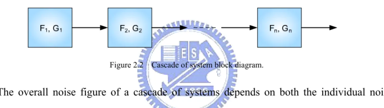
Figure 2.2 Cascade of system block diagram.
The overall noise figure of a cascade of systems depends on both the individual noise figures as well as their gains. The dependency on the gain results from the fact that, once the signal has been amplified, the noise of subsequent stages is less important. As a result, system noise figure tends to be dominated by the noise performance of the first several stages in a receiver. Consider the block diagram of Figure 2.2, where each is the noise figure and each is the gain. The total noise factor is the sum of these individual contributions, and is therefore given by
Chapter 2 Basic Concepts of LNA Design
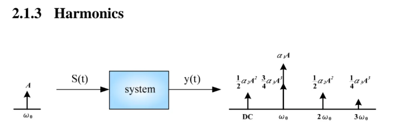
2.1.3 Harmonics
Figure 2.3 Frequency response of nonlinear system with one tone signal.
In wireless receiver, the low-noise amplifier usually can be approximately treated as linear system for processing small signal. In fact, it is nonlinear and the input-output relationship of a nonlinear system can be described by
, (2.11) Here, as shown in Figure 2.3, S(t) is the input signal, and y(t) is the output signal. Using the function (2.11) with one tone signal at the input, cos , the output of the nonlinear system can be viewed mathematically as
cos cos cos
α cosω cos2ω cos3ω . (2.12)
As can be seen easily from (2.12), harmonic distortion is generated and is defined as the ratio of the amplitude of a particular harmonic to that of the fundamental. For example, third-order harmonic distortion (HD3) is defined as the ratio of amplitude of the tone at 3
to that of the fundamental at , and is therefore given by
Chapter 2 Basic Concepts of LNA Design
2.1.4 1-dB Gain Compression Point (P1dB)
Figure 2.4 Definition of 1-dB compression point.
As can be seen easily from (2.12), for an amplifier, the output amplitude of the fundamental will not be given with a linear gain (α1) when the input signal amplitude is large.
We rewrite only the term of the fundamental as follows
t α cosω α cosω . (2.14)
At this point, from (2.14), α3 is usually negative, and the gain will be compressed while
the input signal amplitude exceeds some value. In RF circuits, this effect is quantified by the “1-dB compression point,” defined as the input signal level that causes the linear small-signal gain to drop by 1 dB. It is depicted graphically in Figure 2.4. To calculate the 1-dB compression point, we can write from (2.14)
20log α ‐ 20log|α | 1dB. (2.15) That is,
Chapter 2 Basic Concepts of LNA Design
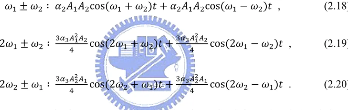
2.1.5 Inter-Modulation
As more than one tone is applied to a nonlinear system, Inter-modulation (IM) arises. Assume that there are two strong interferers occurred at the input of the receiver, specified by cos cos . The IM distortion can be expressed mathematically by applying to (2.11)
cos cos
cos cos
cos cos (2.17) Using trigonometric manipulations, we can find expressions for the second and the third-order IM products as follows
cos cos , (2.18)
2 cos 2 cos 2 , (2.19)
2 cos 2 cos 2 . (2.20)
The output spectrum in frequency domain can be determined from (2.18)-(2.20) by evaluating its Fourier transform. In a typical two-tone test, , there are two third-order IM products at 2 and 2 respectively, and then the output signal will be corrupted by one of the two, illustrated in Figure 2.5.
Chapter 2 Basic Concepts of LNA Design
2.1.6 Third-Order Intercept Point (IP3)
The corruption of signals due to third-order IM of two nearby interferes is so common and so critical that a performance has been defined to characterize this behavior. Called the “third intercept point” (IP3), this parameter is measured by a two-tone test in which the input amplitude ( ) is chosen to be sufficiently small so that higher-order nonlinear terms are negligible and the gain is relatively constant and equal to α1. From (2.19) and (2.20), we note
that as A increases, the fundamentals increase in proportion to , whereas the third-order IM products increase in proportion to . Plotted on a logarithmic scale in Figure 2.6, the third-order intercept point IP3 is defined to be the intersection of the two dotted lines elongated from linear region. Therefore, we can see that the amplitude of the input interferer at the third-order intercept point, , is d nefi ed by th r la n e e tio
20 log α 20log α . (2.21) From (2.21), we can solve for AIP3:
. (2.22) For 50-Ω systems, we define the input third-order intercept point (IIP3) as IIP3
IIP /50. (IIP3 is hence interpreted as the power level of the input interferer at the
third-order intercept point).
Chapter 2 Basic Concepts of LNA Design
2.2 Conventional Wideband Input Impedance Matching
Architecture
In wireless receivers, low-noise amplifier is the first stage in the front-end RF circuits and is used to amplify the received weak signal with low noise figure and good input impedance match. However, a tradeoff among the input impedance match, die area, power consumption and noise figure of LNA should be carefully studied. There are several 50-Ohm input-matching architectures that have been explored in the conventional wideband CMOS LNA shown in Figure 2.7. In this section, we will introduce these architectures which can be achieved wideband input impedance match.
(e) Inductive degeneration with transformer
K
Zin
Zg
Zin
(d) Inductive source degeneration with broadband pass filter (a) Resistor termination
Zin (c) 1/gm termination Zin (b) Shunt-shunt feedback Zin RFC Zin (f) Distributed amplifier Term. Term.
Chapter 2 Basic Concepts of LNA Design
2.2.1 Resistor Termination Architecture
Resistive termination architecture is the most straightforward approach to achieve the wideband 50-Ohm match at the input shown in Figure 2.8. The resistor equal to (=50 Ohm) is placed across the input terminal of the LNA to provide the wideband impedance match.
Figure2.8 Resistor termination architecture.
Usually, the input-matching bandwidth of this approach determined by the input capacitance of the transistor is very broad, due to the pole associated with the input at very high frequency. Unfortunately, the resistor R placed at the input not only adds thermal noise but also attenuates signal (by a factor of 2) ahead of the transistor. Consequently, the combination of these two effects generally produces unacceptably high noise figure. More formally, it is straightforward to establish the following lower bound on the noise figure of this circuit (neglecting gate current noise):
/ / g /g / /
/ 2 g , (2.23)
where , / , is the drain-source conductance at zero , and is the channel thermal noise coefficient. Therefore, it seems that there is a tradeoff between the performance of the input impedance match and the noise figure.
Due to the high noise figure, the resistor termination architecture is not practical in most wireless application even though the input-matching bandwidth is very broad.
Chapter 2 Basic Concepts of LNA Design
2.2.2 Shunt-Series Resistor Feedback Architecture
The resistor feedback technique is used to achieve a good input-match shown in Figure 2.9, [5], [8]. This technique unlike resistor terminating, it does not attenuate the signal by a noisy resistor before reaching the input (gate) of transistor and hence the noise figure is expected to be better than that of the case of resistor termination.
Figure 2.9 Shunt-series re tor feedback architecture. sis
However, not only the feedback resistor ( ) continues to generate thermal noise of its own, but it also has no good input-output isolation. Furthermore, due to the negative-feedback, the gain will be sacrificed for bandwidth enhancement.
2.2.3
Common-Gate Architecture (
/
Termination)
Using the common-gate configuration shown in Figure 2.9 can provide wideband input impedance match by designing 1/ that is equal to 50 Ohm, [6], [9], [10].
Figure 2.10 Common-gate architecture.
Similarly, the input-matching bandwidth of this approach is determined by the input capacitance of the transistor, but we can suppress the capacitive effect by means of parallel inductor LS to enlarge wider input-matching bandwidth, and it provides the DC path for
Chapter 2 Basic Concepts of LNA Design
transistor operating. The input impedance is given by
g g . (2.24)
The real part of the input impedance 1/gm must be of 50 Ohm to provide the input match,
and the is limited to the value of 20m A/V2. This value usually leads to lower gain than that of the other approaches and lightly high noise figure. However, common-gate architecture has the highest potential to achieve the wideband input impedance match, good linearity, and input-output isolation.
It is straightforward to establish the following lower bond on the noise figure of the common-gate amplifier (neglecting gate current noise):
g /g 1
. (2.25) It is about 2.2dB for long-channel devices and perhaps as high as 4.8dB for short.
2.2.4
Inductive Source Degeneration with Broadband-Pass Filter
Figure 2.11 Inductive source degeneration architecture.
First, as shown in Figure 2.11, we must introduce the inductive source degeneration that can present a real input impedance to achieve input match without noisy resistor at only one frequency (at resonance) [28]. The input impedance is that of a series RLC network which has the following form,
in g s
gs g
Chapter 2 Basic Concepts of LNA Design
Consequently, the resistance is transformed from an inductor LS, and it does not bring with the
resistive thermal noise because a pure reactance is noiseless.
As a result, this architecture has the highest potential to achieve the narrow-band input impedance match with good noise performance. However, the inductor consumes more die area than would probably be consistent with an economical design.
At resonance, the gate-to-source voltage is Q times as large as the input voltage. The value of the quality factor Q is given by
gs , (2.27)
where ω ( 1/ gs ) is the resonant frequency, and ωT equals to / gs. The overall stage trans-conductance under this condition is therefore
g g
gs . (2.28)
In order to achieve wideband input impedance match, the ladder-LC filter is employed at the input of the amplifier shown in Figure 2.12 [4], [8]. For instance, there are some papers using Butterworth filter [11], Chebyshev filter or others. Therefore, this architecture can provide a wideband input impedance match without substantially adding thermal noise, but we must consider the issue of large die area almost consumed by numerous inductor.
Chapter 2 Basic Concepts of LNA Design
2.2.5
Inductive Source Degeneration with Transformer
To achieve the wideband input impedance match with low noise, the inductive source degeneration with broadband pass filter has been introduced already. However, due to this technique exploiting numerous inductors, the die area is always larger than that of other techniques. For this reason, the inductive source degeneration with transformer (or called the mutual inductor) architecture is developed to reduce die area for the wideband input impedance match shown in Figure 2.13.
Figure 2.13 Inductive source degeneration with a transformer.
From Figure 2.13, the ideal coupling factor K is equal to constant unity, but this factor is dependent on frequency and smaller than unity actually. Then, K will be a function of frequency, and the input impedance may possibly have more than one resonant frequency to achieve the wideband input impedance match.
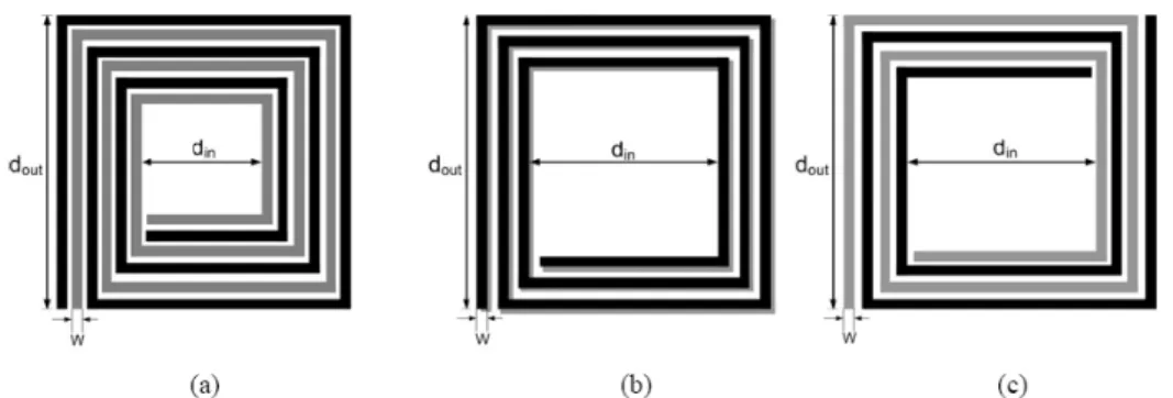
However, although this technique can save the die area efficiently, the implementation and modeling of mutual inductor (two coupling inductors) is so complicated due to effects of the parasitic capacitance between the one inductor and the other. Several examples of Layout of mutual inductor is shown in Figure 2.14.
Figure 2.14 Layout of various mutual inductors. (a) Parallel (Shibata) configuration. (b) Overlay (Finlay) configuration. (c) Inter wound (Frlan) configuration.
Chapter 2 Basic Concepts of LNA Design
2.2.6 Distributed Amplifier
Another architecture which can achieve very broadband input impedance match is the distributed amplifier shown in Figure 2.15. This technique, exploiting several inductors with the input capacitance of MOSFET forms equivalently a transmission-line model whose characteristic impedance is of 50Ω, and it is terminated by a 50-Ω resistor.
Although the architecture can achieve very broadband input impedance match, the numerous stages cause much power consumption. Consequently, this architecture is usually not practical for wireless portable devices.
Figure 2.15 Distributed amplifier.
2.2.7
Comparison of Wideband Input Matching Architectures
The comparison of wideband input-matching architectures is shown in Table 2.1. Table 2.1 Comparison of wideband input matching architectures
Input-matching architecture Advantage Drawback
Wideband input
impedance match.
Chapter 2 Basic Concepts of LNA Design
Wideband input
impedance match.
Wideband frequency response.
High power dissipation.
Poor reverse isolation.
Feedback resistor gives rise to thermal noise.
Wideband input impedance match. Good linearity. Good reverse isolation. No Miller effect.
Lower power gain.
Higher noise figure.
Wideband input-
impedance match.
Low noise figure.
Good power gain.
Large area.
Low noise figure.
Good power gain.
Hard to design.
Complicated design.
The best wideband input-matching.
Good frequency response.
Large area
Chapter 2 Basic Concepts of LNA Design
2.3 Methods to Reduce Noise Figure of LNA
In order to obtain acceptable signal-to-noise ratio (SNR), noise figure should be performed as lower as possible in LNA design. There are several methods to reduce noise figure.
2.3.1
Gate-Drain Overlap Capacitance Neutraliz tion Method
a
The negative feedback from the gate-drain overlap capacitance ( ) cannot be ignored in the high frequency, which leads to degradation of input impedance match, noise figure and gain. This feedback effect (called Miller effect) can be reduced using an inductor that mitigates the reactance of the parasitic capacitance .
Chapter 2 Basic Concepts of LNA Design
2.3.2
Miller Effect Mitigation by Using Cascode Configuration
Although using the inductor can cancel the effect of the parasitic capacitance , it may not be necessary and suitable for on-chip implementations. That another technique can mitigate miller effect is using cascade configuration shown in Figure 2.17.
Figure 2.17 Miller effect mitigation by using cascode configuration.
2.3.3
Feed-Forward Thermal Noise Canceling Method
Figure 2.18 illustrates that cancel the channel thermal noise of with straightforward implementation using an ideal feed-forward voltage amplifier with a gain ( 0) [13].
Figure 2.18 Feed-forward thermal noise canceling architecture
Chapter 2 Basic Concepts of LNA Design
terms of that of node Y
X, Y, S/ S . (2.29) The output noise voltage due to the oise n of the atch ng m i device, , is then equal to
, Y, X,
1 S/ S . (2.30)
Y,
Thus, the output noise cancellation, , 0, is achieved as the gain AV equal to
1 S/ . (2.31)
2.3.4
Input-Matching Device Thermal Noise Reduction Method by
Using Mutual Inductor
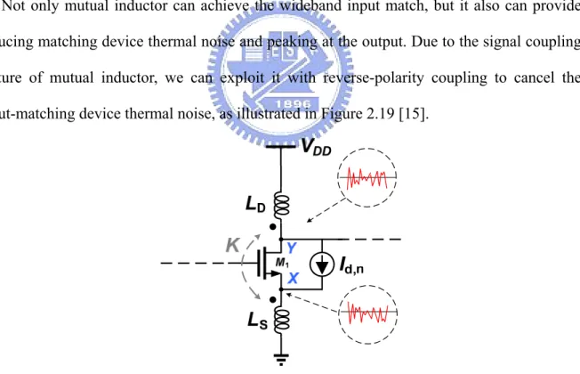
Not only mutual inductor can achieve the wideband input match, but it also can provide reducing matching device thermal noise and peaking at the output. Due to the signal coupling feature of mutual inductor, we can exploit it with reverse-polarity coupling to cancel the input-matching device thermal noise, as illustrated in Figure 2.19 [15].
Figure 2.19 Thermal noise reduction using a mutual inductor
From Figure 2.19, the thermal noise voltage due to the input-matching device M1 in
magnitude at node X with self inductance is
Chapter 2 Basic Concepts of LNA Design
and the thermal noise voltage in magn udeit at node Y with self inductance is
Y, , , (2.33)
Thus, the output noise reduction achiis eved
, α , X, Y,
, α , , (2.33)
where K is the coupling coefficient of the mu al indu or, and N is the turn ratio. tu ct
By proper design of parameters of and , we can reduce the output thermal noise due to input-matching device M1. Furthermore, input-matching purpose inductor
and output-peaking purpose are fabricated together to form a mutual inductor, so it reduce the chip area efficiently. However, the implementation of mutual inductor is so complicated due to effects of the parasitic capacitance between the one inductor and the other.
2.3.5
Quality Factor (Q) of Inductor Enhancement Method
In order to achieve that gain and noise is not degraded by parasitic resistance of inductors at the input of LNA; we should require the high-Q inductor to improve the gain and noise figure shown in Figure 2.20.
Figure 2.20 Inductive source degeneration architecture requires high-Q inductor.
A new implementation of high quality factor (Q) copper inductor on CMOS silicon substrate using a fully process is presented. The Q factor of such inductors depends on the
Chapter 2 Basic Concepts of LNA Design
conductivity of metal layer and other parasitic components. Planner spirals can be of different shapes, i.e. square, hexagonal, octagonal and circular as shown in Figure 2.21.
Chapter 2 Basic Concepts of LNA Design
2.4 Considerations of LNA Design
In general, the following should be considered in LNA design:
a. Input- and Output-matching:
In wireless receiver, the component placed before LNA is usually the filter and antenna with characteristic impedance 50 Ω, so the input impedance of LNA must be matched to obtain high input/output return loss.
b. Low Noise Figure:
The noise figure of the entire receiver system is almost dominated by the first building block, LNA. Thus, noise figure of LNA is the most important parameter to evaluate the noise performance of the entire receiver system. And we should know that there is a tradeoff among the performance of the input match, noise figure and power consumption, etc.
c. Sufficient power gain and bandwidth:
The sufficient power gain of the LNA is also important, because not only it amplifies the receiver RF signal but it also compresses the noise contribution from the sequential stages. Thus, the design of LNA with an insufficient gain, the noise performance of the entire receiver system may not be excellent even if noise figure of LNA is small.
d. Low power consumption:
The power consumption is crucial to the designs of RF circuits, especially for portable device. Thus, no matter what RF circuits we design, the DC power should be consumed as lower as possible with acceptable performance.
Chapter 3 Review of Low-Power LNA Designs
Chapter 3 Review of Low-Power LNA Designs
3.1 Introduction
In LNA designs, that there are some low-power consumption techniques have been proposed, such as
a. Reduce or save supply current: Current-reused technique,
Common-gate configuration with non-50-Ω input impedance technique, Gain boost using mutual inductor technique.
b. Reduce supply voltage:
Forward body bias technique,
Chapter 3 Review of Low-Power LNA Designs
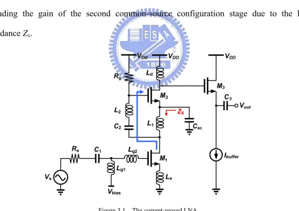
3.2 Current-Reused Technique
The current-reused LNA is composed of two common-source configuration stages under the common-current structure that can save the power consumption effectively, as shown in Figure 3.1. As can be seen from this Figure, in order to achieve the current-reused structure with two common-source configuration stages, we must exploit an inductor L1 which is
employed for passing the DC current and blocking the AC signal into the source of M2, and
then, we lead the signal to reach the gate of M2 to achieve the second common-source
configuration stage. Furthermore, not only does inductor L1 block the signal into the source of M2, but it also peaks the output of the first common-source configuration stage by cancelling
the parasitic capacitance at the drain of M1. And the bypass capacitor Cac is used to avoid
degrading the gain of the second common-source configuration stage due to the large impedance Zx.
Figure 3.1 The current-reused LNA.
However, in order to achieve wideband input matching (Lg1, Lg2 and LS), signal blocking
(L1) and inductive peaking (Ld) network, we must use more than five inductors which result in
Chapter 3 Review of Low-Power LNA Designs
3.3 Common-Gate Configuration with Non-50-Ω Input
Impedance Technique
The common-gate architecture has the highest potential to achieve the wideband input impedance match. In the conventional common-gate LNA design, as shown in Figure 3.2(a), the resistance looking into the source terminal of M1 is 1/gm, which should be equal to 50 Ω
(gm=20m A/V2) to provide the wideband input impedance match.
At this point, we introduce an approach that can save half the power consumption of the conventional common-gate LNA. The low-power common-gate LNA is shown in Figure 3.2(b). In order to achieve low power consumption, we make the resistance looking into the source terminal of M1, 1/gm, be equal to 70.7 Ω that can reduce half the current while 1/gm is
equal to 50 Ω, since we know that the (1/gm)2 is inversely proportional to the current Id from
the well-known relation given by
g 2µc WL . (3.1) Although we can reduce the power consumption by this method, it causes the input impedance mismatch with RS (50 Ω). So the impedance must be transformed by incorporating
the reactance component.
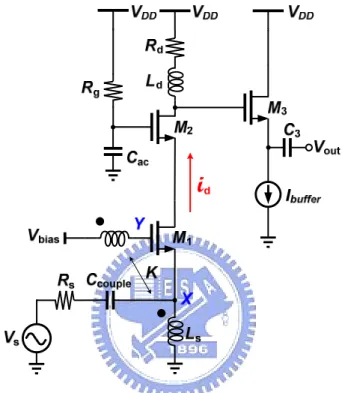
Rs Vs Vbias Ls Ccouple M1 Vout VDD VDD VDD Ibuffer M2 M3 C3 Cac Rg Ld Rd ZS ≈1/gm=50 Ω Id
Chapter 3 Review of Low-Power LNA Designs
3.4 Gain Boost by Using Mutual Inductor Technique
In LNA design, we usually utilize the multistage architecture if the gain is inadequate to amplify the weak received signal. However, the multistage architecture will consume much DC power that is not suitable for the low-power applications.
Figure 3.3 Gain boost by using mutual inductor technique.
For this reason, a gain boost approach that can increase the gain without any power consumption has been proposed by utilizing a mutual inductor, as shown in Figure 3.3. The mutual inductor is used to increase the gate-source small-signal voltage that converts high small-signal current to obtain the high gain. From Figure 3.3, assumed that mutual inductor is ideal, K=1, we can obtain VY=–VX, thus Vgs=–2 VX. It doubles the gate-source small-signal
voltage compared with Figure 3.2 (a), and then the drain small-signal current would be double too. Therefore, it increases the gain without trans-conductor enhancement that may consume more power.
Chapter 3 Review of Low-Power LNA Designs
3.5 Forward Body Bias Technique
Most performances of LNA which include the gain, noise figure and I/O impedance matching, etc., are dependent on bias current. The higher gain and low noise figure we achieve, the larger current we require. For this reason, reducing the current to achieve low power consumption is not the best method.
In recent years, an approach that can achieve low power consumption by reduced supply voltage has been proposed [x], called the forward body bias (FBB). While a forward voltage biases the P-N junction between the bulk (or called the body) and source terminal of MOSFET, the P-N junction depletion region can be reduced, and then the minor carrier charge in the substrate can be attracted to create the channel under the lower gate-source and drain-source voltage than that of MOSFET without FBB.
We use the theoretical formula to explain why gate-source and drain-source voltage can be reduced maintaining the same current with FBB technique. The well-known threshold voltage formula is given by
2 2
where is the threshold voltage at zero bulk-source voltage, the Fermi level deep in the bulk, and γ denotes the body effect coefficient. From (3.2), biasing the bulk-source P-N , (3.2)
junction forwardly to reduce the P-N junction depletion region means that the threshold voltage can be reduced. Since the threshold voltage is reduced by using FBB, the gate-source and drain-source voltage can be lowered with the constant current, as known from the MOSFETs current equation
Chapter 3 Review of Low-Power LNA Designs
3.6 Dynamic-Threshold Voltage Technique
Although the FBB technique can reduce supply voltage to achieve low-power consumption, the voltage biased the bulk-source terminal requires an additional bias circuit (or called the voltage reference circuit) to supply it. The additional bias circuit consumes the DC power as well, so the FBB technique may not actually achieve low-power consumption. Therefore, the dynamic-threshold voltage approach that improves the FBB technique has been proposed. Since the gate-source bias voltage is always required to let MOSFET work as an amplifier, the bulk terminal can directly connect with the gate terminal to obtain bulk-source voltage that saves an additional bias circuit, as shown in Figure 3.4.
Figure 3.4 Low-power design with the dynamic-threshold voltage technique.
However, it has a troublesome issue with noise while using the dynamic-threshold voltage technique. Because, at the gate terminal in the first stage, the received weak signal has not amplified yet, the considerable thermal noise in the substrate will significantly degrade the noise figure if the bulk and gate terminal connect together in the first stage of LNA. Therefore, we proposed the self forward body bias technique in the next chapter that need not employ an additional bias circuit and doesn’t degrade the noise figure significantly.
Chapter 3 Review of Low-Power LNA Designs
3.7 Comparison of Low-Power consumption Techniques
The comparison of low-power consumption technique is shown in Table 3.1.Table 3.1 Comparison of low-power consumption techniques.
Low-power technique Advantage Drawback
Current-reused High gain. Low noise. Large area. Hardly design. Poor linearity. Common-gate configuration with non-50-Ω input imped- ance
Good linearity.
Wideband input impedance matching.
Low gain
Noise figure degradation.
Gain boost using mutual in- ductor High gain. Wideband input impedance matching. Low noise. Hardly implement an mutual inductor.
Forward Body Bias
High gain
Wideband input impedance matching.
Require an additional bias circuit.
Dynamic-Threshold voltage
High gain
Wideband input impedance matching.
Thermal noise in the substrate significantly degrades noise figure.
Chapter 4 Design of Low-Power SFBB UWB LNA
Chapter 4 Design of Low-Power Self-Forward-Body-Bias
UWB LNA
4.1 Introduction
A low-power UWB LNA we proposed is achieved by using self-forward bulk-source bias. And the forward bulk-source voltage in our design is obtained by means of the proposed ultra-low power self-bias that we don’t need an additional bias circuit to supply the bulk terminal of MOSFET. However, the self forward body bias technique will give rise to some noise figure degradation. Therefore, we proposed the second LNA (LNA 2) to improve the noise figure of the preceding LNA (LNA 1) in this chapter. The measurement result shows that the LNA 1 has a gain of 12.5–15.5 dB from 2.6 to 6.6 GHz with a good input/output matching S11<-10 dB and S22<-17 dB and average noise figure of 3 dB while consuming
power of 6.3 mW from 1.06 V voltage supply. And the measurement result of the LNA 2 shows that it has a gain of 13.5–16.2 dB from 2.0 to 6.6 GHz with a good input/output matching S11<-10 dB and S22<-16 dB and average noise figure of 2.4 dB while consuming
Chapter 4 Design of Low-Power SFBB UWB LNA
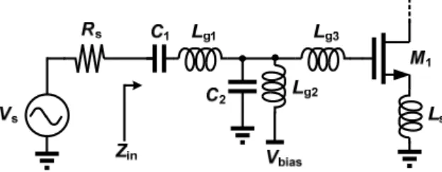
4.2 The Proposed Low-Power UWB LNA
The proposed low-power CMOS LNA for 3–6.5 GHz is show in Figure 4.1. It consists of two stages and the output buffer. The first stage using the complementary architecture amplifies the received weak signal with wideband input impedance matching and low noise figure, and the second stage employs the cascode architecture to compensate the gain at high frequency band of interest 3–6.5 GHz.
Figure 4.1 The proposed low-power SFBB UWB LNA.
The low-power technique in our LNA design is by means of self forward body bias (SFBB) which we first proposed. We will introduce and analysis the SFBB technique in this section.
4.2.1 Design of Input/Output Impedance Matching
In LNA design, the first stage has to provide impedance matching at the input. In order to achieve low noise and wideband impedance matching, we utilize a complementary architecture with two inductive source degenerations in parallel, as shown in Figure 4.2, and
Chapter 4 Design of Low-Power SFBB UWB LNA
the input small signal equivalent circuit is shown in Figure 4.3.
Rf M1 M2 LS1 LS2 R1 Ccouple VDD Rs Vs 1st. stage Series-RLC1 Series-RLC2
Figure 4.2 The first stage of the proposed low-power SFBB UWB LNA.
Figure 4.3 Equivalent circuit of the input impedance.
From Figure 4.3, that both the inductive source degenerations in parallel with different resonant frequencies design and with low Q factor can provide a wideband input matching in the first stage in our LNA design. Further, the resistance of the series-RLC1 and series-RLC2,
gm1LS1/Cgs1 and gm2LS2/Cgs2, result from the transformation of the inductor and transistor.
Therefore, both the resistances do not give rise to thermal noise, so the inductive source degeneration is a superior matching topology for low noise design. In addition to both the inductive source degenerations, there is a resistance, RM =Rf /(1-Av) in across the input and
ground due to Miller effect, which Rf is employed to supply gate-source self bias ,and Av
Chapter 4 Design of Low-Power SFBB UWB LNA
inductive source degenerations and resistor feedback, the input impedance is
Z s || s || , s s s 1 s 1 s || , 1 1 1 s 1 s || . (4.1) Finally, the simulated and measured impedance matching response (S11) of the first stage
in our LNA design is depicted in Figure 4.4.
0 1 2 3 4 5 6 7 Frequency (GHz) S11(dB) -30 -25 -20 -15 -10 -5
Chapter 4 Design of Low-Power SFBB UWB LNA
4.2.2 Gain Bandwidth Extension
Although the first stage using complementary with two inductive degenerations can provide the wideband input impedance matching with low noise, it cannot provide the sufficient high frequency gain. Therefore, we have to incorporate the second stage that employs the cascode architecture with the inductive peaking to compensate the gain of high frequency in the band of interest as well as increase the inverse isolation, as shown in Figure 4.5.
Figure 4.5 Frequency response of the proposed LNA.
The overall gain of the proposed LNA can be obtained by the product of the gain of the first and second stage. The gain of the first is
m1 o1
o1 1 1 m1 o1 1
m2 o2
o2 1 1 m2 o2 2 1, (4.2)
Chapter 4 Design of Low-Power SFBB UWB LNA
||
1 1 2 2 , (4.3)
and the gain of the second is
|| . (4.3)
4.2.3 Self Forward Body Bias (SFBB) Technique
The low-power technique in our LNA design is by means of self forward body bias (SFBB) which we first proposed. As can been from Figure 4.6, with adifference to conventional FBB technique [21], SFBB using an ultra-low power self bias approach improves the conventional FBB technique which needs additional bias circuit to supply the bulk terminal of MOSFET for obtaining a forward bulk-source bias.
Figure 4.6 (a) Conventional FBB with additional bias circuit. (b) Self-FBB.
In the SFBB approach, as shown in Figure 4.6(b), we can achieve ultra-low power self-bias loop since the P-N junction (parasitic diode) between the bulk and source in the MOSFET is treated as a component in a voltage-divided loop, and only working within at its cut-off region, in which the P-N junction voltage is lower than the cut-in voltage Vcut,in
(typically about 0.5 V). The well-known P-N junction I-V characteristic equation is given by 1 , (4.4)
Chapter 4 Design of Low-Power SFBB UWB LNA
where is the ideality factor, is the thermal voltage, and denotes the reverse-bias leakage current. Applying the cut-off region (0 < < ), the current through the P-N junction is very small (about few μA) that leads a self-bias loop with ultra-low power consumption (about few μW).
,
Figure 4.7 (a) The first stage with the MOSFET model. (b) Self-bias voltage-divided loop.
The ultra-low power self-bias loop employed in the two stages of the proposed LNA is analyzed and evaluated as follows. In Figure 4.7(a), the first stage using the complementary architecture that consists of an N-MOSFET and a P-MOSFET is shown. In order to provide the bulk-source P-N junction voltage ( and ) of both the transistors to form a voltage-divided loop with forward bias, a resistor is employed to connect the bulk terminal of and that of . To be simple, the self-bias voltage-divided loop is individually shown in Figure 4.7(b). In the loop, is properly selected to yield the bulk-source P-N cut-off region, which can achieve ultra-low power self-bias loop. The formula of is derived as follows, which start with the voltage equation of the self-bias voltage-divided loop,
Chapter 4 Design of Low-Power SFBB UWB LNA
According to (4.4), the loop current is expressed in terms of or ,
1 , (4.6) or 1 . (4.7) Here, and denote the reverse-biased leakage current of the bulk-source P-N junction of the N-MOSFET and P-MOSFET in the first stage respectively. Then, substituting (4.6) into (4.5), we obtain 1 , (4.8) thus, . (4.9) (a) (b) VDD R2 VBS4 = VDS4 VBS3 + +
-I
2 Ld Cgs4 Cgs3 Cgd4 Cgd3 G3D3 S4 B3 B4 VDD Id2-I2-Ibs4 Id2-I2 Rd G4 D4 S3 R2 RdI
2 VDB4 + -VBS4 M3 NMOS M4 NMOS + -VBS3 VBD3 0 +-I
d2 Id2-I2-Ibs4 Id2-I2Figure 4.8 (a) The second stage with the MOSFET model. (b) Self-bias voltage-divided loop.
The second stage uses the cascode architecture shown in Figure 4.8. Similarly, in order to form a self-bias loop, we exploit a resistor to connect between their bulk terminals. The principle and analysis method of the SFBB technique in the second stage is similar to that of the first stage, so we only show what the value of we need while the bulk-source P-N
Chapter 4 Design of Low-Power SFBB UWB LNA
junction voltage, , is operating within cut-off region. And is equal to (about 0.45 V), so it also works within cut-off region.
_
. (4.10)
Vcut,in> VB> 0
(a) Without forward body Bias (b) With forward body Bias
P
substraten+ n+
p+
B
ulkS
ourceG
ateD
rainSiO2 Depletion region VD> 0 VG> 0
P
substrate n+ n+ p+B
ulkS
ourceG
ateD
rainSiO2
Depletion region
VG> 0 VD> 0
Figure 4.9 MOSFET (a) without forward body bias, (b) with forward body bias technique.
Finally, we have to explain why the threshold voltage and supply voltage can be lowered while we obtain the forward bulk-source bias. The N-MOSFET without and with forward body bias is shown in Figure 4.9(a) and Figure 4.9(b) respectively. As can be seen, if the P-N junction between the bulk and source terminal is biased by forward voltage, the depletion between N-channel and P-substrate will be narrower than that of without forward bias. Then, while the depletion is shrunk, the electron in the P-substrate is easier to be attracted than that
Chapter 4 Design of Low-Power SFBB UWB LNA
of N-MOSFET without forward bias under the same gate-source and drain-source voltage. Therefore, the threshold voltage is reduced by means of forward bulk-source bias, and the formula of threshold voltage is given by
2 2 , (4.11) where is the threshold voltage at zero bulk-source voltage, the Fermi level deep in the bulk, and γ denotes the body effect coefficient. And the gate-source and drain-source voltage can be lowered than that of N-MOSFET without forward bulk-source bias for the same current, as known from the MOSFETs current equation
1 λ . (4.12) And Figure 4.10 illustrates that the threshold voltage with forward bulk-source bias compares with that of zero bulk-source voltage by simulation. The threshold voltage of the MOSFET with =0 V is about 0.45 V; and that of the MOSFET with =0.45 V is about 0.35 V.
Chapter 4 Design of Low-Power SFBB UWB LNA
4.2.4 Noise Analysis of The Proposed LNA
Before analyze the noise figure of the proposed LNA (Figure 4.1), we have to draw the circuit with noise sources shown in Figure 4.11.
Figure 4.11 The proposed LNA with noise sources. The noise factor is defined as:
. (4.13) As equation (4.12) shows that the noise factor equals to the ratio of total output noise and output noise due to source. The noise sources in the LNA contain the resistor thermal noise, channel thermal noise, induced gate noise (correlated and uncorrelated with channel thermal noise), gate resistive thermal noise and bulk thermal noise, etc. In order to simply estimate, we assume that the passive components are ideal without other parasitic effects. At the first, we start with the calculation of the output noise power spectrum density (PSD) due to the input source resistor ,
Chapter 4 Design of Low-Power SFBB UWB LNA
, 4 | | , (4.14)
where , and are expressed in (4.1), (4.2) and (4.3) respectively. The noises PSD contributed by the part of the induced gate noise in and that are fully uncorrelated with the drain channel thermal noise:
, , , ω || || || , | | 1 | | , (4.15) , , , ω || || || , | | 1 | | s , (4.16) where , s , , , , , , , , 1 ω || 1 ω || || ,
and and c are the induced gate noise coefficient and correlation coefficient. The output noise PSD due to correlated induced gate noise source and drain channel thermal noise source of and :
, , , , , , , , ,
, , , , , 2 , , , , , , (4.17)
, , , , , , , , ,
Chapter 4 Design of Low-Power SFBB UWB LNA where , , , , , , , | | ω || || || , | | , , , and , , , , , | | ω || || || , | | , , , .
Notice that, in (4.17) and (4.18), the power spectrum densities (PSDs), and , , , should be absolutely positive. The output noise due to , and :
, , , 4 , | | . (4.19)
The output noise due to :
, 4 || || ,
, | | . (4.20)
The noise contributed by the part of the induced gate noise in that is fully uncorrelated with the drain channel thermal noise:
, , , out1,2
2
| | . (4.21) The output noise due to correlated induced gate noise source and channel thermal noise source of , , , , , , , , , , , , , , 2 , , , , , , , . (4.22) where | | , , , , | | | |.
Chapter 4 Design of Low-Power SFBB UWB LNA
Notice that, in (4.21), the power spectrum density (PSD) , , , should be absolutely positive. The thermal noise of the resistor can be suppressed significantly by the gain of the preceding stages, so we neglect this calculation for it. Finally, according to (4.22), the noise factor of the proposed LNA can be expressed as
1 . . . . . . . . (4.23)
4.2.5 Layout Consideration
In radio-frequency integrated circuit designs, not only is the well circuit design essential, but the layout is also considerable. The bad layout may give rise to the poor noise figure and/or the parasitic capacitance that degrades the gain significantly. Therefore, the metal line length, especially near the input, should be as short as possible to minimize the noise figure. In the vicinity of the input in our LNA design is shown in Figure 4.12. From this figure, we can see that the metal line length is short (< 50 μm) near the input pad.
Figure 4.12 Layout near the input pad. Figure 4.13 RF pad wi/wo the grounded metal-1 layer. Another issue that also degrades the noise figure results from the input RF pad. As can be seen from Figure 4.13, a lot of thermal noise exists in the substrate that will be coupled to the input RF pad to degrade noise figure. To overcome this problem, we add the grounded metal-1 (M1) layer that will improve the noise figure efficiently.
Chapter 4 Design of Low-Power SFBB UWB LNA
4.2.6 Simulation and Measurement Result
The simulated results of the LNA with SFBB technique compare with that of the LNA without SFBB technique.
The simulated input impedance matching (S11) with and without SFBB technique are
shown in Figure 4.14 and Figure 4.15 respectively:
0 1 2 3 4 5 6 7 Frequency (GHz) S11(dB) -20 -15 -10 -5
Figure 4.14 Simulated S11 (input impedance matching) with SFBB technique.
Chapter 4 Design of Low-Power SFBB UWB LNA
The simulated reverse isolation (S12) with and without SFBB technique are shown in
Figure 4.16 and Figure 4.17 respectively:
Figure 4.16 Simulated S12 (reverse isolation) with SFBB technique.
Chapter 4 Design of Low-Power SFBB UWB LNA
The simulated gain (S21) with and without SFBB technique are shown in Figure 4.18 and
Figure 4.19 respectively:
Figure 4.18 Simulated S21 (gain) with SFBB technique.
0 1 2 3 4 5 6 7 Frequency (GHz) S21(dB) 0 5 15 10 20 25 30 -5
Chapter 4 Design of Low-Power SFBB UWB LNA
The simulated output impedance matching (S22) with and without SFBB technique are
shown in Figure 4.20 and Figure 4.21 respectively:
Figure 4.20 Simulated S21 (output impedance matching) with SFBB technique.
0 1 2 3 4 5 6 7 Frequency (GHz) S22(dB) -19 -18 -17 -16 -16 -15 without SFBB