適用於光子積體晶粒之多模光波導交叉元件及彎轉鏡面耦合器
133
0
0
全文
(2)
(3)
(4)
(5)
(6) 致 謝. 在中山大學的研究生生涯中,首先要感謝啟蒙老師張道源博士, 再者是費心指導我的教授賴聰賢博士,他們提供我一個非常良好的學 習環境,讓我能夠確實經歷實驗室的規劃建置、機台的安裝維修及實 驗的設計製作..等流程;更由衷感謝 2006 年本人在美國貝爾實驗室 實習時有幸得到陳陽闓博士的耐心協助。最後要感謝出席學生博士論 文口試的委員們及莊順連博士能在百忙中抽空出席旁聽我的口試,您 們的指導與建議,使我的論文更加地完整與紮實。 特別要謝謝馮瑞陽同學在晶片成長的材料提供,使我有充份的晶 片以製作我的元件,還有歷屆及現任【量子元件暨分子束磊晶實驗室】 學弟妹的付出。 最終,我要感謝始終陪在身旁的最親愛的家人們給我精神上的支 持與愛護及總是永遠默默在背後支持我最大功臣老婆–靖惠。.
(7) 摘 要 本論文主要是在磷化銦的半導體光放大器之結構上設計和製作主動與 被動積體化元件。研究內容包含脊狀雷射、量子井混合技術以及製作 1x1 和 2x2 光轉換器與環形共振腔結合多模光波導彎轉鏡面耦合器。我們發現 當二個多模光波導交叉在自我成像位置時,有最小的擾動。利用有限時域 差分法(FDTD)模擬獲得多模光波導以 90 度或者 60 度交叉在中心位置都 有最小的交錯損失。進而以對稱對摺原理,可在交叉位置形成全反射鏡面, 造成入射光模彎轉進入交叉波導。實際上,為了達到內部全反射有一個 Goos-Hanchen 位移校正在這反射器上並且被一個平面所取代。 被動元件係利用發光波長為 λ=1.41 微米的晶片來製作 1x1 60 度、1x1 90 度、2x2 90 度多模干涉垂直鏡面反射耦合器和環形共振腔結合 2x2 90 度多模干涉垂直鏡面反射耦合器之半導體光濾波器。(1)利用乾式蝕刻技術 來製作在垂直鏡面產生全反射之深蝕刻,並且為了降低內部全反射鏡面損 失我們加入 Goos-Hanchen 位移來校正這反射鏡,藉由垂直鏡面的設計及深 蝕刻鏡面製作,使一入射至多模干涉耦合器的多模光波導轉彎,並在適當 的改變多模干涉耦合器的長度,以達到所需要 85:15 的分光比。(2)在固 定耦合器寬度之下垂直鏡面反射耦合器為傳統多模干涉耦合器之長度縮短 33%,(3)應用這樣耦合器於環形共振腔之光濾波器之共振腔長縮短 50%。 (4)在元件的特性量測方面,2x2 90 度模干涉垂直鏡面反射耦合器量測得.
(8) 到 85:15 的分光效果,並將這樣耦合器應用於環形共振腔之光濾波器可以 得到自由空間的光譜範圍(FSR) 82 GHz 的光譜圖。(5)這樣的單環共振器 分別都被實現以磷化銦為基板,藉由分子束磊晶沉積法的砷化鎵銦/砷化鎵 鋁銦材料及藉由有機金屬化學氣相沉積法的磷砷化鎵銦材料。 為將主動及被動元件積體整合在一個晶片上的需要,我們也發展了量 子井混合技術。第一個方法是在 λ=1.55 微米的晶片,利用氬離子電漿轟擊 後接著快速回火,在這製程過程後的樣品之光激螢光的強度比原來的樣品 變強 10 倍以上並且有少量的 15 奈米藍移。第二個方法是使用 λ=1.55 微米 的晶片,利用氬離子電漿轟擊跟隨濺鍍二氧化矽膜在晶片上接著快速回 火,在這樣製程過程後樣品在磷砷化鎵銦材料得到 90 奈米藍移,並且得到 多重量子井和上方覆蓋層之間的最佳距離是 300 奈米。另外,此方法在砷 化鋁鎵銦材料得到 60 奈米藍移並且在轟擊後多重量子井和上方覆蓋層之 間的最佳距離是 200 奈米。這些結果對於光子積體化的重新成長、可犧牲 層的距離和積體整合製程都是非常有用。.
(9) Abstract In this thesis, ridge waveguide laser, quantum well intermixing, 1x1 and 2x2 optical switching and ring resonator with multimode-waveguide turning mirror couplers have been investigated. We develop a new design that the perturbation is the minimum when the crossing occurs at the self-image location in a low-loss multimode waveguide. We use a center-fold low-loss multimode waveguide with a single self image at the center. Such waveguides can cross at 90 degrees or 60 degrees at the center with minimal cross talk. One can reflect the incident mode into an intersecting waveguide by introducing an idea reflecting plane. In practice, the reflector is replaced by a plane for total internal reflection with correction for Goos-Hanchen shift. Passive component for λ = 1.41 μm samples, 1x1 60-degree multimode-waveguide turning mirror, 1x1 90-degree multimode-waveguide turning mirror, 2x2 90-degree multimode-waveguide. turning. mirror. and. a. multimode-waveguide. turning. mirror. couplers. single. ring. resonator. have. been. fabricated.. with. 2x2. (1). The. multimode-waveguide turning mirror coupler with cross coupling factor (K) of 0.15 is achieved by an etched facet with a correction for Goos-Hanchen shift. (2) The length of the multimode-waveguide turning mirror coupler is only 33% of the length of conventional straight 2x2 MMI coupler with K=0.15. (3) The circumference of the curve waveguide in this ring resonator is decreased by 50%. (4) The characterization of the InP-based single ring resonator incorporating 2x2 multimode-waveguide turning mirror couplers with K= 0.15 has a free spectral range of 82 GHz, a contrast of 4 dB, and a full-width at half-maximum (FWHM). of. 0.24. nm. for. In0.53Ga0.47As/In0.53Ga0.26Al0.21As. the. drop. grown. port.. by. (5). This. single. molecular. beam. epitaxy. resonators (MBE),. in and. In0.67Ga0.33As0.6P0.4/In0.71Ga0.29As0.74P0.26 grown by metal organic chemical vapor deposition (MOCVD) have been demonstrated, respectively..
(10) We have also developed quantum well intermixing technique for the photonic integration. (1) Argon plasma bombardment followed by rapid thermal annealing for InGaAs/InGaAlAs multiple-quantum-well structures grown by MBE has been found to strongly enhance the intensity of room-temperature photoluminescence signal by more than an order of magnitude. The strength of the photoluminescence signal is found to be dependent on the plasma RF power and bombardment time. The resulting blue shift of the photoluminescence wavelength due to quantum well intermixing is found to be under 15 nm. (2) Process combining inductively-coupled-plasma reactive ion etching (ICP-RIE) and SiO2 sputtering film has been investigated for the InGaAsP and InGaAlAs multi-quantum wells (MQWs). Optimal distance is of 300 nm for InGaAsP, and of 200-nm-thick for InGaAlAs between MQWs and the upper cladding by ICP-RIE and bombardment. The process resulted in a bandgap blue-shift of 90 nm for InGaAsP, and of 60 nm for InGaAlAs. The result is very useful to regrown, the sacrificing layer and to integrate the fabrication..
(11) Contents. I. Introduction........................................................................................... 1 1.1 Optical filters .............................................................................................................1 1.2 Ring device applications ............................................................................................4 1.3 Motivation..................................................................................................................5 1.4 Outline of the thesis ...................................................................................................6 Reference ...................................................................................................................7. II. Design of Multimode Waveguide Turning Mirror Couplers --- Analysis, Simulation and Model ..................................................... 9. 2.1 Introduction................................................................................................................9 2.2 Analysis of Coupled Ring Resonators with MMI couplers .......................................11 2.2.1 2.2.2 2.2.3 2.2.4 2.2.5. The transfer functions of a symmetric directional coupler ...........................11 The transfer functions of MMI couplers.......................................................13 Curved waveguide ........................................................................................16 Transfer functions for a double racetrack .....................................................20 Transfer functions for a triple racetrack .......................................................21. 2.3 Simulation and Model................................................................................................22 2.3.1 2.3.2 2.3.3 2.3.4. 1x1 MMI waveguides of 4.4 μm-wide and 5 μm-wide model .....................23 90-degree MMI waveguide crossing and turning mirror model...................24 60-degree MMI waveguide crossing and turning mirror model...................25 2x2 multimode waveguide turning mirror couplers .....................................26. Reference ...................................................................................................................33. I.
(12) III The Material System and Fabrication................................................ 36 3.1 The Material of InGaAlAs .........................................................................................36 3.1.1 3.1.2 3.1.3. The advantage of InGaAlAs .........................................................................36 Compressively Strained QWs .......................................................................38 N-type modulation doping ............................................................................39. 3.2 SOA’s QW..................................................................................................................40 3.2.1 3.2.2. TE-polarized laser.........................................................................................40 p-i-n laser ......................................................................................................42. 3.3 The fabrication of ridge waveguide --- wet etching...................................................47 3.3.1 3.3.2. Multi-step wet etch method ..........................................................................47 Multi-step Undercutting Process ..................................................................50. 3.3.3. Planarization and metal process....................................................................52. 3.4 The fabrication of the waveguides ----dry etching ....................................................53 3.4.1 3.4.2. The curved waveguide ..................................................................................56 The process of the fabricated waveguide......................................................60. 3.5 Multimode interference turning mirror coupler.........................................................66 3.5.1. The fabrication of MMI waveguide crossing and turning mirror.................66. 3.6 Ring resonator with MMI turning mirrors .................................................................67 3.6.1. Single ring device with MMI turning mirrors in InGaAsP material.............68. Reference ...................................................................................................................71. IV Experimental results and Discussion .................................................. 73 4.1 PL and EL measurement.............................................................................................73 4.2 Active devices ............................................................................................................74 II.
(13) 4.3 Passive devices ...........................................................................................................75 4.3.1 4.3.2 4.3.3 4.3.4 4.3.5 4.3.6 4.3.7. Curved waveguides loss................................................................................75 1x1 MMI waveguides of 4.4 μm-wide and 5 μm-wide pattern ....................80 90-degree MMI waveguide crossing and turning mirror pattern..................81 60-degree MMI waveguide crossing and turning mirror pattern..................82 2x2 90-degree MMI waveguide turning mirror pattern................................83 Experimental results with single ring device in InGaAs material ................84 Experimental results with single ring device in InGaAsP material ..............85. Reference ...................................................................................................................88. V. Summary ............................................................................................... 89. APPENDIX - A Quantum Well Intermixing Technique ....................................................... 93 A.1 Introduction ...............................................................................................................93 A.2 Argon plasma induced photoluminescence enhancement .........................................96 A.2.1. Experimental Results ...................................................................................97. A.3 Argon Plasma Bombardment and SiO2 Sputtering Deposition .................................100 A.2.1. Experimental results.....................................................................................102. Reference ...................................................................................................................110. Publication List ......................................................................................... 112. III.
(14) List of Tables TABLE 2.1. The layer sequence of the devices .................................................................22. TABLE 2.2. MMI lengths for three split ratios, w=2.2 μm and Wmmi=7.6 μm ...............30. TABLE 3.1. Structure details of MD3QW .........................................................................45. TABLE 3.2. The epi-layer structure of the waveguide.......................................................54. TABLE 3.3. The layer sequence of the devices in InGaAsP..............................................68. TABLE 4.1. The measured value for bend waveguides and straight waveguides .............80. TABLE A.1. Schematic cross section for the In0.77Ga0.23As0.79P0.21 / In0.57Ga0.43As0.64P0.36 MQWs ..........................................................................................................101. TABLE A.2. Schematic cross section of the epitaxial layer structures for the In0.53Ga0.47As / In0.53Ga0.26Al0.21As MQWs ..........................................................................101. IV.
(15) List of Figures Figure 1.1. Add / Drop filter applications in a simplified WDM system ...........................1. Figure 1.2. A Mach-Zehnder interferometer: (a) free space propagation (b) waveguide device ...............................................................................................................2. Figure 1.3. A Fabry-Perot interferometer: (a) free-space propagation (b) waveguide device .............................................................................................................3. Figure 2.1. Schematic diagram of the general racetrack ring resonator for single racetrack with MMI couplers ......................................................................................17. Figure 2.2. Simulated through and drop port power of this resonator with 3-dB MMI couplers and K=0.15 MMI couplers for the TE polarization.......................19. Figure 2.3. Simulated through and drop port power of this resonator with MMI couplers (K=0.15) and with MMI turning mirror couplers (K=0.15) for the TE polarization ..................................................................................................20. Figure 2.4. Schematic diagram of the general racetrack ring resonator for double racetrack with MMI couplers ......................................................................................21. Figure 2.5. (a) 1x1 MMI waveguide model (b) 1x1 MMI waveguide: width of 5 μm, L mmi = (3/2)L π = 112 μm and the output power is 0.98 (c) 1x1 MMI waveguide: width of 4.4 μm , Lmmi= (3/2)Lπ= 88 μm, and the output power is 0.94...............................................................................................................23. Figure 2.6. (a) 1x1 90-degree MMI crossings model (b) 1x1 MMI width of 5 μm, Lmmi= (3/2)Lπ= 112 μm, L1 is 90-degree crossing position. The crossing at L1= Lmmi/2 location represents the perturbation is the minimum for TE and TM modes. (c) 1x1 90-degree MMI crossing is fixed at the center location, Lmmi scans from 104 μm to 120 μm (step: 4 μm) for TE mode. (d) 1x1 90-degree MMI crossing pattern is at L1= 56 μm, and the output power is 0.96 for TE mode .........................................................................................24. Figure 2.7. (a) 1x1 60-degree MMI crossings model; (b) 1x1 MMI width of 4.4 μm, Lmmi= (3/2)Lπ= 88 μm, L1 is the 60-degree crossing position. The crossing at L1= Llmi/2 location represents the perturbation is the minimum for TE mode. (c) 1x1 60-degree MMI crossing at the center location, Lmmi scans from 80 μm to 96 μm (step: 4 μm) for TE mode. (d) 60-degree crossings at the center location and the output power is 0.94 for TE mode ....................26. V.
(16) Figure 2.8. (a) 2x2 90-degree MMI crossing model (b) 2x2 MMI width of 7.6 μm, scanning Lmmi:125~132μm, step:1μm. The crossing occurs at the middle location (Lmmi=(3/4) L π =128 μm) represents the perturbation is the minimum. The total insertion loss is 5% at Lmmi=128 μm (c) 2x2 90-degree MMI crossing is at center location and the cross/bar output power ratio is 0.85/0.15. (d) 2-D FDTD simulation in the 2x2 MMI turning mirror with a. Figure 2.9. width of 7.6 μm, a length of 128 μm and a gap of 1.6 μm for TM modes. The the bar /cross output power ratio is 0.67/0.12 nearly equal in 0.85/0.15 .......27 (a) scan the Lmmi versus output power in a 2x2 MMI (K=0.15) coupler with a width of 7.6 μm, Lmmi=3*(3/4) Lπ and the input/output port is located at We/4 from the edge. The total insertion loss is 6% at Lmmi=384 μm. (b) the power splitting ratio as a function of wavelength for TE mode in two different 2x2 MMI couplers with a length of (3/4)L π and 3*(3/4)L π , respectively ....................................................................................................29. Figure 2.10 The 2x2 MMI coupler (K=0.85) with a width of 10 μm, Lmmi= (3/4) Lπ= 216 μm and the input/output port is located at We/4 from the edge. the cross/bar output power ratio is 0.85/0.15 ......................................................................31 Figure 2.11 2x2 90-degree MMI crossing with a width of 10 μm, Lmmi= 216 μm is at center location and the cross/bar output power ratio is 0.85/0.15 .................32 Figure 2.12 2-D FDTD simulation in the 2x2 MMI turning mirror with a width of 10 μm, a length of 216 μm and a gap of 2.8 μm for TM mode. The the bar /cross output power ratio is 0.78/0.14 nearly equal in 0.85/0.15 .............................32 Figure 3.1. Diagram of Bandgap vs. lattice constant for various III-V semiconductor at room temperature (after Tien, 1988) ..........................................................37. Figure 3.2. For 1.55-μm wavelength transition, an illustration shows the advantages of lattice-matched InGaAs QW with 1eV InGaAlAs barriers vs. 1eV InGaAsP barriers .........................................................................................................38. Figure 3.3. For 1.55 μm wavelength transition, an illustration shows the advantages of 1% compressive-strained InGaAs QW vs. lattice-matched one with 1eV InGaAlAs barriers..........................................................................................39. Figure 3.4. Strain dependent bandgap parameters for the strained InGaAs single QW with lattice-matched InGaAlAs (Eg = 1eV) barrier and the well width is set such that the energy transition wavelength of e1-hh1 (ε|| < 0) or e1-lh1 (ε|| > 0) is 1.55 μm: (a) quantized energy position (e1, hh1, and lh1), (b) QW thickness and wavefunction overlap integral squared, (c) the inverse out-of-plane effective mass, and (d) the inverse in-plane effective mass...........................41 VI.
(17) Figure 3.5. Schematic diagram for (a) p-i-n laser/SOA’s structure and (b) band diagram .43. Figure 3.6. The refractive index distribution of MD3QW in the transverse direction (y, perpendicular to epi-layers) and its E-field expansion of fundamental slab TE-mode ........................................................................................................44. Figure 3.7. Ridge waveguide laser with width = 2 μm and etching depth = 1.79 μm; (a) the near-field map of fundamental cross-section TE-mode, and (b) its far-field pattern; (c) the divergence of far-field mode pattern in the lateral direction, and (d) in the transverse direction..................................................................46. Figure 3.8. Multi-step wet etch method diagram................................................................48. Figure 3.9. SEM of Multi-step wet etch waveguide ...........................................................49. Figure 3.10 The cross-section SEM for the sidewall of the device patterns after the four steps wet etch process and the HBr solution dipped......................................49 Figure 3.11 Double layer photoresist (OCG825/AZ4210) ..................................................51 Figure 3.12 The cross section of SEM picture after planarization process .........................53 Figure 3.13 The fundamental mode profile of the waveguide operating at λ= 1.55 μm .....55 Figure 3.14 Effective refractive index as a function of the ridge width at λ= 1.55 μm.......56 Figure 3.15 Curved waveguide transferred to a straight waveguide using conformal mapping..........................................................................................................57 Figure 3.16 Calculated bending losses of the waveguide with the outer deep etching .......59 Figure 3.17 The asymmetric structure of the waveguide in the curvature region ...............60 Figure 3.18 Deposition of the SiO2 layer.............................................................................60 Figure 3.19 Deposition of the photoresist............................................................................61 Figure 3.20 The building of SiO2 layer................................................................................61 Figure 3.21 The dry etching of the waveguide ....................................................................62 Figure 3.22 Preparation of the waveguide for the deep etching process .............................63 Figure 3.23 Waveguide in the curve region with deep etching ...........................................63 Figure 3.24 The electron microscope (SEM) photograph of the waveguide with deep etching............................................................................................................64 Figure 3.25 SEM photograph of a waveguide .....................................................................65. VII.
(18) Figure 3.26. SEM photograph of a curved waveguide .......................................................65. Figure 3.27. SEM photograph of a waveguide in the curvature .........................................65. Figure 3.28. (a) Model for a single-ring resonator (b) SEM picture for a single ring resonator.......................................................................................................67. Figure 3.29. (a) SEM photograph for MMI turning mirrors (b) The deepest vertical reflector of MMI.........................................................................................................68. Figure 3.30. SEM photograph (a) for the sidewall of the straight waveguide (b) for the outer side of the curve waveguide (c) for the deepest vertical reflector of MMI.........................................................................................................70. Figure 4.1. PL spectrum of the sample emitted at 1.41 μm at room temperature ............73. Figure 4.2. EL spectra of the sample emitted at 1.41 μm at room temperature ...............74. Figure 4.3. Measurement setup for the characterization of the devices ...........................75. Figure 4.4. The Fabry-Perot resonator is for the straight waveguide with the width of 2.2 μm and the length of 2000 μm...............................................................77. Figure 4.5. The design patterns of the cured waveguide ..................................................78. Figure 4.6. Calculated theoretical bending losses of the waveguide with outer deep etching and experimental bending losses with and without outer deep etching.......79. Figure 4.7. (a) Fabry-Perot oscillations for straight waveguide of width= 2.2 μm (b) Fabry-Perot oscillations for MMI waveguide of width = 4.4 μm, and Lmmi= (3/2)L = 88 μm. (c) Fabry-Perot oscillations for MMI waveguide width = 5 μm, and Lmmi= (3/2)L = 112 μm ................................................81. Figure 4.8. (a) SEM picture for the 90-degree MMI crossing pattern (MMI waveguide width = 5 μm) (b) Fabry-Perot oscillations for the 90-degree MMI crossing patter (c) SEM picture for the 90-degree MMI turning mirror pattern (d) Fabry-Perot oscillations for the 90-degree MMI turning mirror pattern .....82. Figure 4.9. (a) SEM picture for the 60-degree MMI crossing pattern (MMI waveguide width = 4.4 μm ) (b) Fabry-Perot oscillations for the 60-degree MMI crossing pattern. (c) SEM picture for the 60-degree MMI turning mirror pattern (d) Fabry-Perot oscillations for the 60-degree MMI turning mirror pattern ..........................................................................................................83. Figure 4.10. The cross/bar output power ratio with the 2x2 90-degree MMI turning mirror at the operating various wavelength are measured of almost 0.15/0.85 ......84 VIII.
(19) Figure 4.11. MMI width of 7.6 μm, FSR=83GHz, Δλ/FWHM ~6500 and simulation ......85. Figure 4.12. MMI width of 7.6 μm, FSR=82GHz, Δλ/FWHM ~6461 and simulation......87. Figure A.1. Schematic cross section of the epitaxial layer structures for (a) sample 50d and (b) sample C071 ....................................................................................95. Figure A.2. PL spectra at room temperature of sample 50d for different Ar+ plasma exposure times with Ar gas at 100 sccm flow rate, 80-mtorr working pressure, 480 watt RF power and 250 watt ICP power, and followed by RTA at a temperature of 6200C for 120 sec in 15%H2/85%N2 gas at 100 sccm flow rate. The numbers in parentheses refer to the peak wavelength (left) and peak intensity (right) for the PL signal. The PL signal is enhanced by more than one order of magnitude with a maximum blue shift of 15 nm .......................................................................................................97. Figure A.3. PL spectra at room temperature of sample C071 for different Ar+ plasma exposure times with Ar gas at 100 sccm flow rate, 90 mTorr working pressure, 550 watt RF power and 550 watt ICP power, and followed by RTA at a temperature of 6200C for 120 sec in 15%H2/85%N2 gas at 100 sccm flow rate. The numbers in parentheses refer to the peak wavelength (left) and peak intensity (right) for the PL signal. The PL signal is enhanced by up to 23 times with a maximum blue shift of 15 nm ..............................98. Figure A.4. Experimental results for sample C071 showing the variations of (a) the relative room-temperature PL intensity, and (b) the PL peak wavelength. both are plotted as functions of the Ar plasma exposure time, working pressure and the RF power. Other common experimental parameters include: Ar flow rate of 100 sccm, ICP power of 250 watt and RTA at 6200C for 120 sec in 15%H2/85%N2 gas at 100 sccm flow rate .........................................99. Figure A.5. (a) Only RTA at different temperature of 700, 750 and 800 ℃ for 1min in N2 gas at a flow rate of 100 sccm (b) 300-nm-thick SiO2 by PECVD and RTA (c) 300-nm-thick sputtered SiO2 and RTA (d) the PL spectra of the sample In0.77Ga0.23As0.79P0.21 /In0.57Ga0.43As0.64P0.36 MQWs under different ICP-RIE time and the same annealing temperature of 800 ℃ for 1 min. at room temperature ..................................................................................................104. Figure A.6. Blue-shift versus annealing temperature under different ICP-RIE time .......105. Figure A.7. (a) DCXRD spectra of the InGaAsP as-grown and the 90-nm-blueshifting samples (b) Simulation calculated the heavy-hole and light-hole band diagram for InGaAsP as-grown and the 90-nm-blueshifting samples .........106 IX.
(20) Figure A.8. (a) The PL spectra at room temperature of the sample In 0.53 Ga 0.47 As /In0.53Ga0.26Al0.21As MQWs under different ICP-RIE time and the same annealing temperature of 700 ℃ for 1 min. in N2 gas at a flow rate of 100 sccm (b) Blue-shift versus annealing temperature under different ICP-RIE time ..............................................................................................................108. Figure A.9. (a) PL spectra by ICP-RIE for 8 minutes without SiO2 capping layer under the annealing temperature 700 and 750 ℃ (b) PL spectra of InGaAlAs samples using H3PO4 solution wet etching to replace ICP-RIE dry etching ...................................................................................................109. X.
(21) Chapter I. Introduction. 1.1 Optical filters Optical switching and routing are highly desirable performance in optical communication networks. [1.1] The main role of optical fibers has long distance to transmit high-speed bit streams from point to point between nodes in the network. An optical fiber could carry 4, 8, 16, 32 or more optical channels at different wavelengths. Optical filters are a controlling light technology for wavelength division multiplexing (WDM) systems. The WDM systems require single routing and coupling devices to have large bandwidth and to be polarization insensitive. The most obvious application is for demultiplexing very closely spaced channel waveguides. However, a simplified WDM system showing one direction of signal transmission is outlined in Fig. 1.1. Multiplexing and demultiplexing filters are found in the terminals. A filter referred to as an add/drop filter is required to separate the channel to be dropped from those that pass through unaffected. Node 1 receives the dropped channel and may transmit its own information on a new signal at the same wavelength as that dropped or a new wavelength that does not interfere with those already used by the other channels on the throughput.. Fig. 1.1 Add/Drop filter applications in a simplified WDM system. 1.
(22) An incoming signal is split into a number of parts that are individually split and then recombined. The optical characterization is found in interferometers. Optical filters (interferometers) come in two general classes, although there are many variations of each. The first class is simply displayed by the Mach–Zehnder interferometer (MZI). This filter consists of a pair of couplers connected by two paths of unequal optical length. i.e., an incoming signal is split equally into two optical paths. The effective group velocity dispersion used for the optical paths of different lengths results that some wavelengths are output to the Out1 and the other wavelengths are output to the Out2. The signals in the two paths are then recombined as shown in Fig. 1.2(a). A partially reflecting mirror indicated by the dashed line, acts as a beam splitter and combiner. A 2x2 waveguides with directional couplers for the splitter and combiner is shown in Fig. 1.2(b). Each implementation has two outputs that are power complementary. The interfering paths are always feeding forward even though the interferometer may be folded such as with a Michelson interferometer. The signal processing used to design this filter type is classified as moving average (MA) or finite impulse response (FIR).. Fig. 1.2 A Mach-Zehnder interferometer: (a) free space propagation (b) waveguide device.. 2.
(23) The second class of interferometers is displayed by the Fabry–Perot interferometer (FPI). The FPI consists of a cavity surrounded by two highly reflective parallel mirrors separated by a small distance as shown in Fig. 1.3(a). The frequency response depends on the spacing and index of refraction between the mirrors, at some wavelengths the multiple reflections interfere constructively. At these wavelengths the interferometer’s overall transmission is low and the overall reflectivity is high. The planar waveguide is a ring resonator with two directional couplers as shown in Fig. 1.3(b). There are two outputs: Out2 corresponds to the transmission response of the FPI and Out1 corresponds to its reflection response. The signal processing filters with feedback paths are classified as autoregressive (AR) or infinite impulse response (IIR) filters.. Fig. 1.3 A Fabry-Perot interferometer (a) free-space propagation (b) waveguide device. The fundamental relationships between optical waveguide and digital filters were developed by Moslehi et al. [1.2] in 1984. Both digital and optical filters consist of splitters, delays and combiners. These parts are identified in Fig. 1.2 and 1.3 for the MZI and FPI, respectively. Thin film and Bragg grating filter design and fabrication are nature, having well established design techniques. [1.3-1.5] Theses filters are important devices because nearly 3.
(24) square bandpass filter response can be achieved with a short filter length. The first optical waveguide filters were achieved using optical fibers and discrete components such as tapered fused-fiber couplers for splitters and combiners. The FSR was small and the surrounding fluctuations changed the optical path difference significantly. It was advantage of using a source with a coherence length shorter than the unit delay (the optical path lengths are typically integer multiples of the smallest path length difference. the smallest path length is called the unit delay length.) so that the combining functions were linear in intensity instead of the field. In this case, referred to as incoherent processing, the filter operates on the modulated signal on an optical carrier. Only positive filter factors are achievable, limiting the filter response to low pass designs. Optical MA filters using fiber delay lines were first proposed for high-speed correlators and pulse compression by Wilner et al. [1.6] in 1976. For AR filters, E. A. Marcatili proposed using an integrated ring resonator for a bandpass filter [1.7] in 1969 is interesting. The fabrication of planar waveguide has been critical for waveguide filters. In particular, low loss and process control, whereby fabricated devices closely approximate the design intent, enable the successful integration of multi-stage filters on a chip. The first coherent MA filter was demonstrated in 1984 using optical fibers. [1.8] The first multi-stage planar waveguide coherent MA filter was demonstrated in 1991 [1.9], and the first coherent multi-stage AR filter was demonstrated in 1996. [1.10]. 1.2 Ring device applications Optical ring waveguide resonators are a useful component for wavelength filtering, multiplexing, switching and modulation [1.11, 1.12]. There has been a growing interest in the application of multimode interference (MMI) couplers in photonic integrated circuits (PICs). For example, dense wavelength division multiplexing (DWDM) communication systems require different kinds of wavelength selective devices which may de-/multiplex closely 4.
(25) spaced channels. An optical filter is needed to provide add/drop ports to select and drop the desirable channel while letting pass-through channels unaffected [1.13, 1.14]. Ring resonator devices have also been used for many other DWDM applications such as wavelength filtering, routing, switching, modulation and multiplexing /de-multiplexing [1.15, 1.16]. InP-based PICs operating at optical wavelength of λ=1.55 μm are of great research interests for optical communications [1.17, 1.18].. 1.3 Motivation The finesse by Mach-Zehnder interferometer is low and its dimension is large size as high channel spacing requires cascaded devices. Ring resonator with direct couplers or MMI couplers has a nano-functionality and the free spectrum range (FSR) is high. Ring resonator with direct couplers is need to the smaller gap ≦ 0.8 μm. It is very different by photolithography (contact alignment machine) and dry etching the smaller gap region is a challenge. So the MMI coupler is used, the gap is bigger ≧ 1.6 μm and the dry etching is easier (the loading effect is unaffected). For PICs purpose, 1x1 60-degree multimode waveguide (MMI) turning mirror, 1x1 90-degree MMI turning mirror, 2x2 90-degree MMI turning mirror and a single ring resonator with 2x2 MMI turning mirror couplers has been achieved. The MMI turning mirror coupler with cross coupling factor (K) of 0.15 is performed by an etched facet with a correction for Goos-Hanchen shift. The advantage of the MMI turning mirror coupler is only 33% the length of conventional straight 2x2 MMI coupler with K=0.15. Moreover, the circumference of the curve waveguide in this ring resonator is decreased by 50% and the gap between 2x2 input/output waveguides is 1.6 μm for MMI width of 7.6 μm. However, the used conventional straight MMI couplers or direct couplers are either of too large size to reduce the channel spacing, or not feasible for photolithography. This thesis mainly describes a novel design and fabrication of single-ring resonators with low-loss 5.
(26) multimode waveguide turning-mirror couplers.. 1.4 Outline of this thesis The PICs require a monolithic integration of active and passive components such as lasers, semiconductor optical amplifiers (SOAs), electro-absorption modulators (EAMs), ring waveguides, optical couplers, etc., to implement the circuit functionality. One of the fundamental difficulties for monolithic integration is the realization of different semiconductor bandgaps for the active/passive components within one epitaxy wafer. This can be achieved using re-growth, selective area growth [1.19], vertical coupling [1.20] or quantum well intermixing (QWI) [1.21]. The energy bandgap is blue shifted by a typical wavelength space > 80 nm for the passive components [1.22] to reduce direct bandgap absorption. The other issue is to reduce the component dimension and to simplify the fabrication process. Ring-based waveguide interference devices such as resonators, filters are the key components in DWDM system. The analysis and simulation of the single ring resonator with multimode waveguide turning mirrors is presented in chapter Ⅱ. The novel design is developed and researched. It is an important part of the design process. Chapter Ⅲ describes that the composition of the quaternary III-V semiconductor compound InGaAsP or InGaAlAs lattice matched to InP are two main material systems used to fabricate long-wavelength semiconductor lasers. The material is presented the advantage, strain, p-i-n structure…etc. The fabricated process has two methods (wet and dry etching) and the experimental results are presented in chapter Ⅳ. All of these results are summarized in chapter Ⅴ for active, passive devices and quantum well intermixing techniques. Appendix - A develops the quantum well intermixing techniques. This technique can combine the active and passive component to integrate on the chip. 6.
(27) Reference [1.1] J. H. Marsh, O. P. Kowalski, S. D. Macdougall, B. C. Qiu, A. Mckee, C. J. Hamilton, R. M. De La Rue and A. C. Bryce, ”Quantum well intermixing in material system for 1.5 μm,” J. Vac. Sci. Technol., vol. A16, pp. 810-816, 1998. [1.2] B. Moslehi, J. Goodman, M. Tur and H. Shaw, “Numberical methods for optical thin film,” Opt. and Photon. News, pp. 23-33, 1997. [1.3] H. Kogelnik, “Filter Response of Nonuniform Almost-Periodic Structures,” Bell System Techn. J., vol. 55, no. 1, pp. 109–126, 1976. [1.4] H. Macleod, Thin-film Optical Filters. New York: McGraw-Hill, 1989. [1.5] A. Thelen, Design of Optical Interference Coatings. New York: McGraw-Hill, 1989. [1.6] K. Wilner and A. Van den Heuvel, “Fiber-optic delay lines for microwave signal processing,” Proc. IEEE, vol. 64, pp. 805–807, 1976. [1.7] E. Marcatili, “Bends in Optical Dielectric Guides,” Bell System Techn. J., vol. 48, no. 7, pp. 2103–2132, 1969. [1.8] D. Davies and G. James, “Fibre-optic tapped delay line filter employing coherent optical processing,” Electron. Lett., vol. 20, pp. 96–97, 1984. [1.9] K. Sasayama, M. Okuno, and K. Habara, “Coherent Optical Transversal Filter Using Silica-Based Waveguides for High-Speed Signal Processing,” J. Lightw. Technol., vol. 9, no. 10, pp. 1225–1230, 1991. [1.10] C. Madsen and J. Zhao, “A General Planar Waveguide Autoregressive Optical Filter,” J. Lightw. Technol., vol. 14, no. 3, pp. 437–447, 1996. [1.11] K. Oda, S. Suzuki, H. Takahashi, and T. Toda, “An optical FDM distribution experiment using a high finesse waveguide-type double ring resonator,” IEEE Photon. Technol. Lett., vol. 6, pp. 1031-1034, Aug. 1994. [1.12] R. Orta, P. Savi, R. Tascone, and D. Trinchero, “Synthesis of multiple-ring-resonator filter for optical systems,” IEEE Photon. Technol. Lett., vol. 7, pp. 1447-1449, Dec. 1995. [1.13] L.B. Soldano and E.C. M. Pennings, “Optical Multi-mode Interference Device Based on Self-Imaging:Principle and Application,” IEEE Journal of lightwave technol., vol.13, pp.615-627, April 1995. 7.
(28) [1.14] Pierre A. Besse, Emilio Gini, Maurus Bachmann, and Hans Melchior “New 2X2 and 1X3 Multimode Interference Couplers with Free Selection of Power Splitting Ratios” IEEE Journal of lightwave technol., vol.14, pp.2286-2293, Oc t. 1996 [1.15] D.G. Rabus and M. Hamacher, “MMI-Coupled Ring Resonators in GaInAsP-InP,” IEEE Phonton. Technol. Lett., vol. 13, pp.812-814, August 2001. [1.16] D.G. Rabus , M. Hamacher, U. Troppenz, and H. Heidrich, “Optical Filters Based on Ring Resonators With Integrated Semiconductor Optical Amplifiers in GaInAsP-InP” IEEE Journal of Selected Topics in Quantum Electronics, vol. 8, pp.1405-1411, Nov. 2002. [1.17] P. K. Bhattacharya, “Semiconductor Optoelectronic Devices”, Englewood Cliffs, Prentice Hall, NJ, 1998. [1.18] G. P. Agrawal and N. K. Dutta, “Semiconductor Lasers”, Van New York, Nostrand Reinhold, 1993. [1.19] J. J. Coleman, R. M. Lammert, M. L. Osowski and A. M. Jones, “Progress in InGaAs-GaAs selective-area MOCVD toward photonic integrated circuits”, IEEE J. Selected Topics in Quantum Electronics, vol. 3, pp. 874-884, Jun. 1997. [1.20] S. Charbonneau, E. Koteles, P. Poole, J. He, J. Haysom, M. Buchanan, Y. Feng, A. Delage, M. Davies, R. Goldberg, P. Piva, and I. Mitchell, “Photonic integrated circuits fabrication using ion implantation”, IEEE J. Selected Topics Quantum Electronics, vol. 4, pp. 772-793, July 1998. [1.21] N. Cao, B. B. Elenkrigg, J. G. Simmos and D. A. Thompson, “Band-gap blue shift by impurity free vacancu diffusion in strained multiple quantum well laser structure”, Appl. Phys. Lett., vol. 70, pp. 3419-3421, Jun. 1997. [1.22] B. C. Qiu, X. F. Liu, M. L. Ke, H. K. Lee, A. C. Bryce, J. S. Aitchison, J. H. Marsh, and C. B. Button, “Monolithic Fabrication of 2X2 Crosspoint Switches in InGaAs-InAlGaAs Multiple Quantum Wells Using Quantum-Well Intermixing,” IEEE Photon. Technol. Lett., vol.13, pp.1292-1294, Dec. 2001.. 8.
(29) Chapter Ⅱ Design of Multimode Waveguide Turning Mirror Couplers ---- Analysis, Simulation and Model 2.1 Introduction Optical switches providing point-to-point and/or point-to-multipoint connections are important components for signal routing in optical communication networks and photonic integrated circuits (PICs). There has been a growing interest in the application of multimode interference (MMI) effects in PICs. [2.1-2.5] The MMI coupler is an attracting component because of its bandwidth and polarization properties and its tolerance of fabrication variations. [2.1-2.3] Its operation has been demonstrated in Mach-Zenhnder interferometer switches, [2.5, 2.6] and ring resonators. [2.7] For example, dense wavelength division multiplexing (DWDM) systems require different kinds of wavelength selective devices which may de-/multiplex closely spaced channels. Ring resonator devices have already been used for many other DWDM applications such as wavelength filtering, routing, switching, modulation and multiplexing /de-multiplexing applications [2.8-2.11]. Optical waveguide switches provide optical connection between the branching components on the same semiconductor substrate. If the propagation direction of the light-wave signal which spreads optical waveguide is changeable by the acute angle, the accumulation element number per unit area can be increased. The requirements for an optical switch are that it should be lossless, and has a low crosstalk. In this section, the new design of optical switches using MMI effect is demonstrated. The propagation direction can be changeable at 90 or 60 degrees. When two multimode waveguides are made to cross, it can result in significant scattering loss and cross talk due to the perturbation to the edges of the waveguide. We find the perturbation is the minimum when the crossing occurs at self-image location in a multimode waveguide. We use 9.
(30) a center-fold MMI waveguide with a single self-image at the center. One can reflect the incident mode into an intersecting waveguide by introducing an idea reflecting plane. For compactness, the MMI waveguides can be as narrow as twice the width of the access waveguide. Optical ring waveguide resonators are a useful component for wavelength filtering, multiplexing, switching and modulation. [2.17, 2.18] An optical filter is needed to provide add/drop ports to select and drop the desirable channel while letting pass-through channels unaffected. [2.1, 2.3] Ring resonator devices have also been used for many other DWDM applications such as wavelength filtering, routing, switching, modulation and multiplexing /de-multiplexing. [2.7, 2.8] Ⅲ-Ⅴcompound semiconductor optical amplifiers (SOAs) are widely used in electronic and optoelectronic devices. [2.19, 2.20] One of the fundamental difficulties for monolithic integration is the need to realize different semiconductor bandgaps within one epilayer (i-layer). This can be achieved using re-growth, selective area epitaxy [2.21], vertical coupling [2.22] or quantum well intermixing (QWI) [2.23]. Our laboratory is developing a sputtered SiO2 or argon plasma bombardment technique for QWI and a re-growth technique by MBE to modify the bandgap of Ⅲ-Ⅴ quantum-wells (QWs) so that passive and active components can be integrated monolithically. Therefore, Photonic integration is divided into two parts. One is an active component with an emission wavelength of 1.55 μm, and the other is a passive component with a bandgap wavelength blue shifted as far as possible, typically space>80nm, [2.24] so as to reduce direct bandgap absorption. This section also describes a novel design of single-ring resonators with low-loss multimode. waveguide. turning-mirror. couplers.. They. are. implemented. in. In0.53Ga0.47As/In0.53Ga0.26Al0.21As heterostructure waveguides, with bandgap wavelength (λgap) = 1.41 μm on an InP substrate.. 10.
(31) 2.2 Analysis of Coupled Ring Resonator with MMI couplers Ring resonators are coupled to external waveguides through 2X2 couplers. These couplers can either be of the directional coupler type or of the MMI type. We will consider the directional coupler first then the MMI coupler.. 2.2.1. The transfer functions of a symmetric directional coupler Let fr and fl be the normalized wavefunctions of the single mode in the right and left. waveguides respectively when they are not coupled. We shall assume that the two uncoupled waveguides are identical. Let β be the phase constant of each of these uncoupled modes and κ the coupling constant between them in the directional coupler. According to the coupled-mode theory for weakly coupled directional couplers (see text books by Yariv, Coldren and Corzine, or Chuang), the coupling of the modes results in two super modes given by (fr ± fl )/ √2. They are approximations to the true eigen modes of the directional coupler. The phase constants of the supermodes are βs0 = β+κ, and βs1 = β-κ. If light of amplitude A enters the left input port of the directional coupler, both of the supermodes will be excited with the same amplitude of A/√2. The total field that propagates down the directional coupler is given by. F=. ⎫ A ⎧ ⎡ f l +f r ⎤ ⎡ f -f ⎤ exp [ -jβ s0 z ] + ⎢ l r ⎥ exp [ -jβ s1z ] ⎬ ⎨⎢ ⎥ 2 ⎩⎣ 2 ⎦ ⎣ 2⎦ ⎭. =. ⎧ ⎡ f +f ⎤ ⎡ f -f ⎤ ⎫ A exp [ -jβ s0 z ] ⎨ ⎢ l r ⎥ + ⎢ l r ⎥ exp ⎡⎣ -j ( β s1 -βs0 ) z ⎤⎦ ⎬ 2 ⎩⎣ 2 ⎦ ⎣ 2 ⎦ ⎭. =. ⎧ ⎡ f +f ⎤ ⎡ f -f ⎤ ⎫ A exp ⎡⎣ -j ( β +κ ) z ⎤⎦ ⎨ ⎢ l r ⎥ + ⎢ l r ⎥ exp [ j2κ z ] ⎬ 2 ⎩⎣ 2 ⎦ ⎣ 2 ⎦ ⎭. (2.1). At z = 0, equation (1) reduces to F = Afl, which is the assumed input field. At any value of z, the field on the right and left waveguides are given respectively by. 11.
(32) Af r exp ⎡⎣-j ( β +κ ) z ⎤⎦ {1- exp [ j2κ z ] 2 = -Af r ⋅ sin(κ z) ⋅ j ⋅ exp(-jβ z). Fr =. } (2.2). π. = Af r ⋅ sin(κ z) ⋅ exp(-jβ z-j ) 2. and. Af l exp ⎡⎣-j ( β +κ ) z ⎤⎦ {1+ exp [ j2κ z ] 2 = Af l ⋅ cos(κ z) ⋅ exp(-jβ z). Fl =. }. (2.3). The cross and bar transfer functions are then given respectively by. π. H x = sin(κ z) ⋅ exp(-jβ z-j ) 2 ⎡ (β -β ) ⎤ ⎡ (β +β ) π ⎤ = sin ⎢ s0 s1 z ⎥ ⋅ exp ⎢ -j s0 s1 z-j ⎥ 2 2 2⎦ ⎣ ⎦ ⎣ (β -β ) π ⎤ ⎡ (β -β ) ⎤ ⎡ = sin ⎢ s0 s1 z ⎥ ⋅ exp ⎢-jβs0 z+j s0 s1 z-j ⎥ 2 2 2⎦ ⎣ ⎦ ⎣. (2.4). and H b = cos(κ z) ⋅ exp(-jβ z) ⎡ (β -β ) ⎤ ⎡ (β +β ) ⎤ = cos ⎢ s0 s1 z ⎥ ⋅ exp ⎢ -j s0 s1 z ⎥ 2 2 ⎣ ⎦ ⎣ ⎦ (β -β ) ⎤ ⎡ (β -β ) ⎤ ⎡ = cos ⎢ s0 s1 z ⎥ ⋅ exp ⎢ -jβ s0 z+j s0 s1 z ⎥ 2 2 ⎦ ⎣ ⎦ ⎣. (2.5). At z = π/(2κ) = Lπ, we get. H xπ = exp [ -jβs0 Lπ ]. (2.6). H bπ = 0. (2.7). and. At z = Lπ/2, we get H xπ /2 =. ⎡ 1 ⎛L ⋅ exp ⎢-jβs0 ⎜ π 2 ⎝ 2 ⎣. ⎞ π⎤ ⎟ -j ⎥ ⎠ 4⎦. (2.8). H bπ /2 =. ⎡ 1 ⎛L ⎞ π⎤ ⋅ exp ⎢-jβ s0 ⎜ π ⎟ +j ⎥ 2 ⎝ 2 ⎠ 4⎦ ⎣. (2.9). and. 12.
(33) Equations (4) and (5) are often given in the following form with optical loss included. ⎛ α ⎞ ⎛ α ⎞ H x = -j K ⋅ exp ⎜ - pu z-jβ z ⎟ = -j K ⋅ exp ⎜ - pu L-jn u k 0 L ⎟ ⎝ 2 ⎠ ⎝ 2 ⎠ ⎛ α ⎞ ⎛ α ⎞ H b = 1-K ⋅ exp ⎜ - pu z-jβ z ⎟ = 1-K ⋅ exp ⎜ - pu L-jn u k 0 L ⎟ ⎝ 2 ⎠ ⎝ 2 ⎠. (2.10). K = sin(κ L) where K is the power coupling factor of the coupler, αpu is the power attenuation constant in the uncoupled waveguide, L is the length of the coupler, nu is the effective index of the uncoupled waveguide, also being the average of the modal effective indices of the two eigen modes in the coupler, k0 is the vacuum phase constant 2π/λ0.. 2.2.2. The transfer functions of MMI couplers The light that enters an MMI from an input waveguide propagates as a combination of. many modes. Each of the modes propagates with a different phase constant. The phase delay to each of the output waveguides is thus ambiguous. Definite phase delays can only be derived at the exact image locations. [2.3, 2.4] For the 1x2 3-dB coupler, the transfer functions to both of the output ports are the same. It is given by H0 = where β 0 =. 1 exp (-jβ 0 Limage ) 2. 2π n r. λ0. -. πλ0 2 e. 4n r W. (2.11). =. 2π n r. λ0. -. ⎛ λ ⎞ = k0 ⎜ nr - 0 ⎟ 3Lπ 6Lπ ⎠ ⎝. π. (2.12). β0 is the phase constant of the fundamental mode in the MMI waveguide (nr is the effective. index of the slab waveguide from which the MMI waveguide is made and We is the effective width of the MMI waveguide) and Limage = (3/8)Lπ is the exact imaging length. For the lateral TE modes (i.e. TM in the slab), the effective width is related to the physical width of the MMI by. 13.
(34) We = WM +. λ0i. (2.13). 2 π n 2r -n cM. For the lateral TM modes (i.e. TE in the slab), it is given by. We = WM +. λ0i 2 π n 2r -n cM. ⎛ n cM ⎞ ⎜ ⎟ ⎝ nr ⎠. 2. (2.14). For the general 2x2 3-dB coupler, the cross (X) and bar (B) transfer functions are given by H X0 =. 1 π⎞ ⎛ exp ⎜ -jβ 0 Limage + j ⎟ 4⎠ 2 ⎝. (2.15). H B0 =. 1 π⎞ ⎛ exp ⎜ -jβ 0 Limage - j ⎟ 4⎠ 2 ⎝. (2.16). where Limage = (3/2)Lπ in this case. When the input port is located at We/4 from the edge, we get double image at Limage = Lπ/2. For this paired-interference case, we have H X0 =. 1 π⎞ ⎛ exp ⎜ -jβ 0 Limage - j ⎟ 4⎠ 2 ⎝. (2.17). H B0 =. 1 π⎞ ⎛ exp ⎜ -jβ 0 Limage + j ⎟ 4⎠ 2 ⎝. (2.18). which are the same as for the directional coupler. For the 2x2, K = 0.85 (cos2(π/8) to be exact) coupler, they are given by. π⎞ ⎛π ⎞ ⎛ H X0 = cos ⎜ ⎟ exp ⎜ -jβ 0 Limage - j ⎟ 8⎠ ⎝8⎠ ⎝. (2.19). 5π ⎞ ⎛π ⎞ ⎛ H B0 = sin ⎜ ⎟ exp ⎜ -jβ 0 Limage - j ⎟ 8 ⎠ ⎝8⎠ ⎝. (2.20). where Limage = (3/4)Lπ in this case. For the 2x2, K = 0.15 coupler, they are given by 5π ⎞ ⎛π ⎞ ⎛ H X0 = sin ⎜ ⎟ exp ⎜ -jβ 0 Limage + j ⎟ 8 ⎠ ⎝8⎠ ⎝. (2.21). 14.
(35) π⎞ ⎛π ⎞ ⎛ H B0 = cos ⎜ ⎟ exp ⎜ -jβ 0 Limage + j ⎟ 8⎠ ⎝8⎠ ⎝. (2.22). where Limage = (9/4)Lπ in this case. Limage is always a well defined multiple of Lπ. Equation (12) shows that Lπ is given by Lπ =. 4n r We2 3λ0. (2.23). If the device length derives slightly from the exact imaging length either because of a small fabrication error or a small change of the wavelength, then we write L = L image + δ L. (2.24). If the deviation is only due to a deviation in the wavelength, then. δ L = L MMI -Limage = -L MMI. λi -λ0 λi. (2.25). The light propagation within the distance δL can be modeled as the propagation of a Gaussian beam. [2.14] The input and output waveguides can be characterized by the following two normalized parameters 2. n eio - n c2 bn = 2 2 nr - nc. (2.26). where neio = βio/k0 is the effective index of the fundamental mode in the input/output waveguides and nc is the effective index of the lateral claddings, and V=. Wio k 0 n 2r -n c2 2. (2.27). where Wio is the physical width of the input/output waveguides. The field distribution of the fundamental mode in the input and output waveguides can be well approximated by that of a Gaussian beam with a spot size of w0. This spot size is half the mode-field diameter of the waveguide. [2.15] 15.
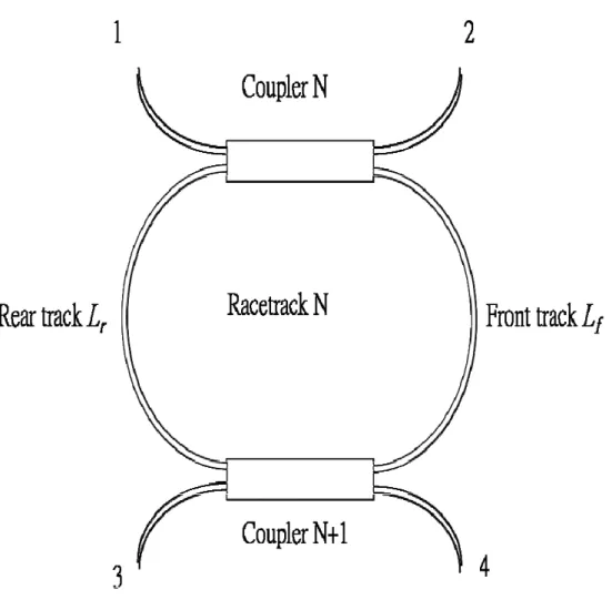
(36) 1/2. 1 ⎞ ⎛ V+ ⎜ ⎛W ⎞ bn ⎟⎟ w 0 = ⎜ io ⎟ ⋅⎜ 3 ⎝ 2 ⎠ ⎜ V (1- bn ) ⎟ ⎜ ⎟ ⎝ ⎠. (2.28). Inside the MMI, Gaussian beam waists with spot size w0 are formed at the input/output and imaging planes. The Rayleigh range around each of the beam waist is given by zR = πw02/λ0. Assuming that the coupling between the neighboring input/output waveguides is negligibly small, the transfer function for finite value of δL is given by. ⎛ ⎛ δ L ⎞⎞ ⎛ 1 + 4Z2 ⎞ H = H0 ⎜ exp ⎜ -j ⋅ k 0 n r ⋅ δ L + j ⋅ tan -1 ⎜ ⎟⎟ 2 4 ⎟ ⎝ 1 + 5Z + 4Z ⎠ ⎝ zR ⎠ ⎠ ⎝ 1/4. (2.29). = H 0 ⋅ mmf ⋅ exp (-jδφ ) where Z =. 2.2.3. δL k 0 n r w 02. and mmf is the mode matching factor. (2.30). Curved waveguide Let us consider the N’th racetrack formed by interconnecting couplers N and N+1 by. a curved front track of length Lf and a rear track of length Lr. (As shown in Fig. 2.1) The transfer function through the length of the front track is given by tf = exp( −α w L f / 2 − j ⋅ n w k 0 L f ). (2.31). where αw is the average power attenuation constant in the waveguide including the bending loss, and nw is the average modal effective index in the waveguide. The transfer function through the length of the rear track is given by tr = exp(−α w Lr / 2 − j ⋅ nw k0 Lr ). (2.32). 16.
(37) Fig. 2.1 Schematic diagram of the general racetrack ring resonator for single racetrack with MMI couplers. The transfer function for one complete loop inside the racetrack N is given by tl N = H B,N ⋅ tf N ⋅ H B,N+1 ⋅ trN. (2.33). The transfer function from input port 1 to drop port 3 is the sum of outputs from successive passes inside the racetrack td N , N +1 = H X,N ⋅ tf N ⋅ H X,N+1 + H X,N ⋅ tf N ⋅ tlN ⋅ H X,N+1 + H X,N ⋅ tf N ⋅ tlN ⋅ H X,N+1 2. + H X,N ⋅ tf N ⋅ tlN ⋅ H X,N+1 + ⋅⋅⋅⋅ 3. =. H X,N ⋅ tf N ⋅ H X,N+1 1 − tlN. (2.34). .. 17.
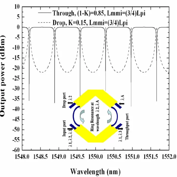
(38) The transfer function from input port 1 to through port 2 is tt N , N +1 = H B,N + H X,N ⋅ tf N ⋅ H B,N+1 ⋅ trN ⋅ H X,N + H X,N ⋅ tf N ⋅ H B,N+1 ⋅ trN ⋅ tlN ⋅ H X,N + H X,N ⋅ tf N ⋅ H B,N+1 ⋅ trN ⋅ tlN ⋅ H X,N + ⋅⋅⋅⋅ 2. H X,N ⋅ tf N ⋅ H B,N+1 ⋅ trN 2. = H B,N +. (2.35). 1 − tlN. H B,N − H B,N ⋅ tlN + H X,N ⋅ tf N ⋅ H B,N+1 ⋅ trN 2. =. 1 − tlN H B,N + (H X,N − H B,N ) ⋅ tf N ⋅ H B,N+1 ⋅ trN 2. =. 2. 1 − tlN. .. For single ring resonator filter, we have obtained the transfer functions for MMI coupler and curve waveguide, so we can calculate the transmitted power at the through and drop port of the racetrack in a single ring resonator. [2.26-2.28] The average power attenuation constant (αw) in the waveguide including bending loss in the ring device is set to 0 cm-1. In these device analysis of MMI and MMI turning mirror, the general design of a single ring resonator with MMI couplers consists of two half-circles, with a radius of 260 μm, connected to two 3-dB MMI couplers or two (K=0.15) MMI couplers jointed at the short straight waveguides. However, the new design of a single ring resonator with MMI turning mirror couplers consists of two 90-degree arc 260 μm radius waveguides connected to two (K=0.15) MMI turning-mirror couplers jointed at short straight waveguides. Comparing only the 50:50 to 85:15 split ratio couplers is of interest to the single- ring resonator. The length of the 3-dB MMI coupler is (3/2)Lπ , but the 85:15 ratio requires a much longer length [3*(3/4)*Lπ]. Therefore, the resonator round-trip length using 85:15 couplers is (3/2)Lπ longer than using 3-dB MMI couplers in the general design. Fig. 2.2 shows the through and drop port power (in dBm) for this resonator with 3-dB MMI couplers and K=0.15 MMI couplers. The free spectral range (FSR) is 0.27 nm for k=0.5 and 0.22 nm for K=0.15. The FWHM linewidth is about 0.08 nm for K=0.5 and 0.02 nm for K=0.15, and the on-off ratio for drop port is about 9.5 dB for K=0.5 and 21 dB for K=0.15. [2.27] From the simulation results, to achieve a narrow FWHM linewidth, K=0.15 MMI coupler is a better choice. 18.
(39) Fig. 2.2 Simulated through and drop port power of this resonator with 3-dB MMI couplers and K=0.15 MMI couplers for the TE polarization.. . When. we achieve high FSR, the cavity length is smaller. The new design concept of. MMI turning-mirror coupler is introduced to this resonator. The length of the MMI turning-mirror coupler (K=0.15) is (3/4)*Lπ and the curve waveguide of this resonator consists of two 90-degree arc-radius waveguides. Fig. 2.3 shows the through and drop port power for the two types of ring resonators with MMI couplers (K=0.15) and with MMI turning mirror couplers (K=0.15). FSR is 0.53 nm, the FWHM is about 0.03 nm, and the on-off ratio for the drop port is about 21dB for MMI turning mirror couplers (K=0.15).. 19.
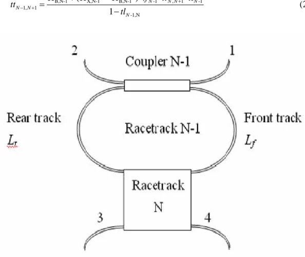
(40) Fig. 2.3 Simulated through and drop port power of this resonator with MMI couplers (K=0.15) and with MMI turning mirror couplers (K=0.15) for the TE polarization.. 2.2.4. Transfer functions for a double racetrack Now let us consider the transfer functions for a double racetrack structure made up of. racetracks N-1 and N. This is the same problem as the single racetrack problem if we replace the role of the coupler N+1 in the previous problem by the racetrack N. (As shown in Fig. 2.4) The transfer function from the input port 1 to the drop port 3 is now given by td N −1, N +1 =. H X,N-1 ⋅ tf N −1 ⋅ td N , N +1 . 1 − tlN −1,N. (2.36). 20.
(41) where the new loop transfer function tlN-1,N involves the participation by the N-th ring. It is given by tlN -1,N = H B,N-1 ⋅ tf N -1 ⋅ tt N,N+1 ⋅ trN-1. (2.37). The transfer function from the input port 1 to the through port 2 is given by H + (H X,N-1 − H B,N-1 ) ⋅ tf N -1 ⋅ tt N , N +1 ⋅ trN -1 tt N −1, N +1 = B,N-1 1 − tlN -1,N 2. 2. (2.38). Fig. 2.4 Schematic diagram of the general racetrack ring resonator for double racetrack with MMI couplers. 2.2.5. Transfer functions for a triple racetrack The scheme described above can be used repeatedly to obtain the transfer functions. for any coupled multiple-racetrack unit. We shall now discuss the case of a coupled triple racetrack for illustrative purpose. First, td3,4 and tt3,4 are calculated according to equations (2.34) and (2.35). Then, td2,4, tl2,3 and tt2,4 are calculated according to equations (2.36), (2.37) and (2.38). The same 21.
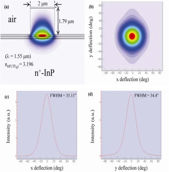
(42) equations are now used to calculate td1,4, tl1,3, and tt1,4 with the tdN,N+1 and ttN,N+1 in the equations replaced by td2,4 and tt2,4. The transfer functions are for field amplitudes. To obtain the power transferred, take the absolute value of the transfer function squared.. TABLE 2.1 The layer sequence of the devices Function. Composition. Thickness (nm). p-contact layer. In0.53Ga0.47As. 60. p-contact grading step. In0.53Ga0.26Al0.21As. 30. p-upper cladding layer 3. In0.52Al0.48As. 500. p-upper cladding layer 2. In0.52Al0.48As. 700. p-upper cladding layer 1. In0.52Al0.48As. 500. i-upper cladding. In0.52Al0.48As. 30. i-region SCH/etch-stop. In0.53Ga0.26Al0.21As. 45. n-side depletion layer. In0.53Ga0.26Al0.21As. 4.5. Active layer (λgap=1.41 μm). four quantum wells. 54.2. Lower SCH layer. In0.53Ga0.26Al0.21As. 40. Lower cladding. In0.52Al0.48As. 100. T(2sec)+10. In0.53Ga0.26Al0.21As. 34. InP substrate. 2.3 Simulation and Model The low-loss multimode waveguide crossings and turning mirror couplers were implemented in In0.53Ga0.47As/In0.53Ga0.26Al0.21As heterostructures. The wafer was of p-i-n structure and grown on n-type InP substrate by solid-source molecular beam epitaxy (MBE). The epi-layer sequence is depicted in Table 2.1. The epitaxial structure has a 54.2-nm thick core layer of InGaAlAs/InGaAs multiple quantum wells (MQWs), which is sandwiched with 1.79-μm top-cladding layer and 0.18-μm bottom-cladding layer (almost InAlAs).. 22.
(43) 2.3.1. 1x1 MMI waveguides of 4.4 μm-wide and 5 μm-wide model To realize passive components in optical wavelength (λ) = 1.55 μm, the band gap. wavelength (λgap) is 1.41 μm for the MQWs to avoid absorption loss. The numerical simulation for the TE-polarized optical wave propagation in the waveguide crossings was carried out by using 3-D beam propagation method (BPM) software. First, the optical transmission at λ = 1.55 μm for the MMI waveguides was studied. The 1x1 MMI waveguides with a width of 5 μm and 4.4 μm were simulated, respectively. The 1x1 MMI waveguide has an in/output single-mode waveguide of 2.2 μm in width. The in/output single-mode waveguide is located at the lateral center of the MMI waveguide, as shown in Fig. 2.5(a). Fig. 2.5(b) shows that the 5-μm-wide MMI waveguide has an output power of 0.98 at the length (Lmmi) of 112 μm, which is equal to the theoretical value of (3/2)Lπ. Here Lπ is the beat length of the two lowest-order modes in the MMI waveguides [2.1]. For the 4.4-μm-wide MMI waveguide, the output power is 0.94 at Lmmi = 88 μm, as shown in Fig. 2.5(c).. Fig. 2.5 (a) 1x1 MMI waveguide model (b) 1x1 MMI waveguide: width of 5 μm, Lmmi= (3/2)Lπ= 112 μm and the output power is 0.98; (c) 1x1 MMI waveguide: width of 4.4 μm , Lmmi= (3/2)Lπ= 88 μm, and the output power is 0.94.. 23.
(44) 2.3.2. 90-degree MMI waveguide crossing and turning mirror model From the simulations, at the middle Lmmi /2 of the 1x1 MMI waveguides, a self image. of the single mode input was reproduced by the MMI effect. As we intersect two MMI waveguides of same dimensions at 90-degree crossing, the MMI waveguide output power will be affected by the intersecting position L1 due to the perturbation of mode-field distributions.. Fig. 2.6 (a) 1x1 90-degree MMI crossings model (b) 1x1 MMI width of 5 μm, Lmmi= (3/2)Lπ= 112 μm, L1 is 90-degree crossing position. The crossing at L1= Lmmi/2 location represents the perturbation is the minimum for TE and TM modes. (c) 1x1 90-degree MMI crossing is fixed at the center location, Lmmi scans from 104 μm to 120 μm (step: 4 μm) for TE mode. (d) 1x1 90-degree MMI crossing pattern is at L1= 56 μm, and the output power is 0.96 for TE mode. 24.
(45) Fig. 2.6(a) shows the two intersecting 1x1 5-μm-wide MMI waveguides and L1 is 90-degree crossing position. The output power as a function of L1/Lmmi from 0.1 to 0.9 (step = 0.05) is shown in Fig. 2.6(b) for TE and TM modes, respectively. The maximum output power was obtained at L1= Lmmi/2 both of TE and TM modes. The output power for TM mode is about 8% less than TE mode, which is ascribed to the less index guiding effect in the growth direction. As the intersecting point is fixed at L1= Lmmi/2, we have simulated the output power by changing the Lmmi from 104 μm to 120 μm at a step of 4μm. The results in Fig. 2.6(c) exhibit a minimum perturbation with 0.96 output power at an optimal Lmmi = 112 μm. The output power distribution for the 1x1 5-μm-wide and 112-μm-long MMI waveguide crossing is shown in Fig. 2.6(d).. 2.3.3. 60-degree MMI waveguide crossing and turning mirror model For the case of 60-degree crossing model, three MMI waveguides were made to. intersect each other at L1, as shown in Fig. 2.7(a). Figs. 2.7(b), (c) and (d) show the TE mode results. The data show a minimum perturbation at L1= Lmmi/2 = 44 μm with a maximum output power of 0.94. The field distribution of the single-mode input waveguides can be well approximated by a Gaussian beam with a spot size of w0, which is half of the mode-field diameter. [2.12] Inside the MMI waveguide, Gaussian beam with spot size w0 are formed at the imaging plane L1. The Rayleigh range around the beam waist is given by zR=πw02/λ. If the crossing location is not near the image plane, the MMI effect will be destroyed and the self image will disappear. The self image only survives if there is very little optical field distributed near the crossing boundaries. However, if the spot size is relatively large such that the edge of the beam waist is too close to the boundaries, then the boundaries can seriously damage the image formation. In the study, MMI waveguides with width = 4.4 μm (60-degree MMI waveguide crossing) and 5 μm (90-degree MMI waveguide crossing) are just wide enough 25.
(46) for our cases. The insertion loss may increase again when the MMI waveguide width is too large because the unguided gap will become much larger than the Rayleigh range [2.1, 2.12] and the optical field will diverge rapidly.. Fig. 2.7 (a) 1x1 60-degree MMI crossings model; (b) 1x1 MMI width of 4.4 μm, Lmmi= (3/2)Lπ= 88 μm, L1 is the 60-degree crossing position. The crossing at L1= Lmmi/2 location represents the perturbation is the minimum for TE mode. (c) 1x1 60-degree MMI crossing at the center location, Lmmi scans from 80 μm to 96 μm (step: 4 μm) for TE mode. (d) 60-degree crossings at the center location and the output power is 0.94 for TE mode.. 2.3.4. 2x2 multimode waveguide turning mirror couplers To minimize the physical size of the PIC, the waveguide rings and loops were. designed to be as compact as possible using a 2x2 MMI turning mirror coupler. The. 26.
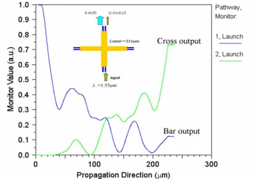
(47) numerical simulation for the TE-polarized mode is performed by using 3-D beam propagation method (BPM) software. The optical transmission at λ = 1.55 μm for the MMI waveguides is studied. First, the 2x2 MMI waveguides with a width of 7.6 μm is simulated.. Fig. 2.8 (a) 2x2 90-degree MMI crossing model (b) 2x2 MMI width of 7.6 μm, scanning Lmmi:125~132μm, step:1μm. The crossing occurs at the middle location (Lmmi=(3/4) Lπ=128 μm) represents the perturbation is the minimum. The total insertion loss is 5% at Lmmi=128 μm (c) 2x2 90-degree MMI crossing is at center location and the cross/bar output power ratio is 0.85/0.15. (d) 2-D FDTD simulation in the 2x2 MMI turning mirror with a width of 7.6 μm, a length of 128 μm and a gap of 1.6 μm for TM modes. The the bar /cross output power ratio is 0.67/0.12 nearly equal in 0.85/0.15. The light that enters an MMI through an input waveguide propagates as a combination of many modes. Each of the modes propagates with a different phase. For an 27.
(48) input port of a 2x2 MMI coupler located at We/4 from the edge and definite phase delays can only be derived at the exact image locations. [2.23, 2.24] For the 2x2 MMI (K=0.85) waveguide has two in/output single-mode waveguides of 2.2 μm in width is located at We/4 from the edge, β0 is the phase constant of the fundamental mode in the MMI waveguide, nr is the effective index of the slab waveguide from which the MMI waveguide is made, We is the effective width of the MMI waveguide and Lmmi = (3/4)Lπ is the exact imaging length. [2.1, 2.2] Here Lπ is the beat length of the two lowest- order modes in the MMI waveguides. [2.1] As two multimode waveguides are crossing each other, a significant scattering loss and crosstalk may be introduced by the perturbed fields at the edges of the waveguides. So the crossing occurs at the middle location in a multimode waveguide, we have simulated the output power by changing the Lmmi from 125 μm to 132 μm at a step of 1 μm. The simulated result in Fig. 2.8(b) shows minimum perturbations can be achieved with the cross/bar output power ratio of 0.85/0.15, and the minimum total insertion loss is 5% at an optimal Lmmi = 128 μm. The cross/bar output power ratio distribution of 0.85/0.15 for the 2x2 7.6-μm-wide and 128-μm-long MMI waveguide crossing is shown in Fig. 2.8(c). However, we use the 2x2 MMI coupler with a cross coupling factor of 0.85 in the reflector design. The 2x2 MMI turning mirror coupler gets the reverse coupling factor. The power ratio of the bar coupling factor is 0.85 while the power ratio of the cross coupling factor is 0.15. The reflector for the TE-polarized optical wave propagation in the 2x2 MMI turning mirror coupler is taken effect by using 2-D finite-difference time-domain (FDTD) method. As 3-D transfers to 2-D, the lateral TE modes approximately equal in TM modes in the slab are used. The 2-D FDTD simulated result in Fig. 2.8(d) shows the bar /cross output power ratio is 0.67/0.12 nearly equal in 0.85/0.15 in the 2x2 MMI turning mirror coupler with a width of 7.6 μm, a length of 128 μm and a gap of 1.6 μm for TM modes.. 28.
(49) Fig. 2.9 (a) scan the Lmmi versus output power in a 2x2 MMI (K=0.15) coupler with a width of 7.6 μm, Lmmi=3*(3/4) Lπ and the input/output port is located at We/4 from the edge. The total insertion loss is 6% at Lmmi=384 μm. (b) the power splitting ratio as a function of wavelength for TE mode in two different 2x2 MMI couplers with a length of (3/4)Lπ and 3*(3/4)Lπ, respectively. The side walls of the MMI section are assumed to be etched down to the substrate to keep the number of confined modes large. The straight waveguide is etched down to the separate confinement hetero-structure (SCH) /etch-stop layer (see Table 2.1). For general MMI coupler, the cross coupling occurs at p*(3Lπ), 3-dB coupling occurs at (1/2)* p*(3Lπ), K=0.85 coupling occurs at (3/4)Lπ , and K=0.15 coupling occurs at 3*(3/4)Lπ , where p is an integer. For a MMI coupler (K=0.15), the cross coupling occurs at 3*(3/4)Lπ , scanning the Lmmi length from 379 μm to 389 μm, the minimum total insertion loss is 6% at Lmmi=384 μm according to the 3-D simulation in Fig. 2.9(a). For a 90-degree MMI crossing coupler (K=0.85) which occurs at (3/4)Lπ , as two multimode waveguides cross each other, significant scattering loss and crosstalk may be introduced by the perturbed fields at the edges of the waveguides. Fig. 2.9(b) shows the power split ratio as a function of wavelength for the TE modes in two different MMI couplers with a length of (3/4)Lπ and 3*(3/4)Lπ, respectively. The coupling factors for the TE modes are the same over the entire wavelength range simulated. Moreover, we obtain that the crossing occurs at (3/8) Lπ , which represents the. 29.
(50) best position for the cross pattern and the cross/bar output power ratio of 0.85/0.15. The simulation shows that minimum perturbation can be achieved when crossing occurs at the middle location in a multimode waveguide. The 2x2 MMI turning mirror coupler gets the reverse coupling factor. (i.e., the power ratio of the bar coupling factor is 0.85 while the power ratio of the cross coupling factor is 0.15). The MMI lengths required to give the three split ratios are summarized in Table 2.2.. TABLE 2.2 MMI lengths for three split ratios, w=2.2 μm and Wmmi=7.6 μm. Wmmi (μm). Lmmi (μm) for 3-dB. Lmmi for 85:15 split. Lmmi for 15:85 split. 7.6. 256. 384. 128. The ring resonators are coupled to external waveguides through 2x2 couplers. These couplers can either be of the directional coupler type or of the MMI type. We use the 2x2 MMI turning mirror instead of a directional coupler, as it provides shorter couple length and the wider gap through 2x2 waveguides. The 2x2 MMI couplers in this ring device individually are MMI coupler with a length of 128 μm, a width of 7.6 μm and a gap of 1.6 μm. In a MMI turning mirror design, the reflector is replaced by a vertical-etched mirror for total internal reflection with a correction for Goos-Hanchen shift at the boundary. [2.1] The location of the vertical reflector is designed to take into account the lateral penetration depth of each mode field. 2x2 MMI turning mirror couplers are incorporated in the ring resonators and the facets of the input and output waveguides are tilted by 7 degrees to avoid Fabry-Perot resonances. To achieve the passive component of 2x2 MMI turning mirror coupler and a high Q factor for the ring resonator, the bandgap wavelength of four ternary quantum wells is λgap = 1.41 μm and total active layer thickness is 0.0542 μm is used. Then, the effective index of the straight waveguide is calculated to be 3.214 at 1.55 μm and the optical confinement factor of 0.09. If high Q factor for the ring resonator is performed, the cross coupling factor (K) needs 30.
數據

+7


相關文件
The first row shows the eyespot with white inner ring, black middle ring, and yellow outer ring in Bicyclus anynana.. The second row provides the eyespot with black inner ring
The coordinate ring of an affine variety is a domain and a finitely generated k-algebra.. Conversely, a domain which is a finitely generated k-algebra is a coordinate ring of an
The coordinate ring of an affine variety is a domain and a finitely generated k-algebra.. Conversely, a domain which is a finitely generated k-algebra is a coordinate ring of an
好了既然 Z[x] 中的 ideal 不一定是 principle ideal 那麼我們就不能學 Proposition 7.2.11 的方法得到 Z[x] 中的 irreducible element 就是 prime element 了..
Accordingly, we reformulate the image deblur- ring problem as a smoothing convex optimization problem, and then apply semi-proximal alternating direction method of multipliers
For the proposed algorithm, we establish a global convergence estimate in terms of the objective value, and moreover present a dual application to the standard SCLP, which leads to
Hence, we have shown the S-duality at the Poisson level for a D3-brane in R-R and NS-NS backgrounds.... Hence, we have shown the S-duality at the Poisson level for a D3-brane in R-R
The Hilbert space of an orbifold field theory [6] is decomposed into twisted sectors H g , that are labelled by the conjugacy classes [g] of the orbifold group, in our case
