InAs/In
1-x
Ga
x
As Composite Channel High Electron
Mobility Transistors for High Speed Applications
Edward Yi Chang1, Chien-I Kuo1, Heng-Tung Hsu2, Chia-Yuan Chang1 1Department of Materials Science and Engineering, National Chiao-Tung University
1
2Department of Communications Engineering, Yuan Ze University
Abstract—80-nm InAs channel HEMTs with different lattice matched sub-channels, In0.53Ga0.47As and In0.7Ga0.3As, have been
fabricated. The device with InAs/ In0.7Ga0.3As composite channel
exhibits high drain current density (1101 mA/mm), and high transconductance (1605 mS/mm) at drain bias VDS = 0.8 V. The
high current gain cutoff frequency (ft) of 360 GHz and maximum
oscillation frequency (fmax) of380 GHz of the device with InAs/
In0.7Ga0.3As were obtained at VDS = 0.7 V in comparison to the
InAs/In0.53Ga0.47 As channel HEMTs with ft = 310 and fmax = 330
GHz. This is due to the high electron mobility and electron confinement in the InAs/ In0.7Ga0.3As channel. In addition, a low
gate delay time 0.84 psec was obtained at VDS = 0.5 V. The
excellent performance of the InAs channel HEMTs demonstrated in this study shows great potential for high speed and very low power logic applications with the optimal design of In0.7Ga0.3As/InAs/In0.7Ga0.3As composite channel.
I. INTRODUCTION
Low DC power consumption devices and circuits have always been desired for all kinds of communications systems especially the satellite communications. With the breakthrough in semiconductor hetero-structure technologies, planar III-V compound semiconductor field effect transistors (FETs) or high electron mobility teansistors (HEMTs) have been identified as one of the most attractive devices for such applications. Besides, in order to extend Moore’s law well into the next decade, III-V based heterostructure devices is also a potential candidate FETs for low-power logic applications beyond Si CMOS technology in 22 nm node era [1-3].
The excellent RF-performance has been demonstrated by InAlAs/InGaAs HEMTs on InP substrate or GaAs substrate [4-6]. In fact, higher electron mobility and velocity can be realized by reducing of gate length (Lg) or increasing of the indium content in the InGaAs channel. Due to the high
electron mobility (~ 20000 cm2/V˙s), high drift velocity,
reasonable energy band gap (0.36 eV), and large conduction band offset in InAs, InAs-channel HEMT is considered very promising for high speed and low power logic applications.
In this study, channel structures of HEMTs with different indium concentration as upper and lower lattice-matched sub-channels, including In0.53Ga0.47As and In0.7Ga0.3As are fabricated and evaluated for the RF and digital performances.
II. EXPERIMENT
The epitaxial structure of the InAs-channel with different In1-xGaxAs cladding layer as the sub-channel (In0.53Ga0.47As and In0.7Ga0.3As) HEMTs were grown by molecular beam epitaxy (MBE) on InP substrate, respectively. These sub-channels were applied to minimize the interface roughness scattering and further enhance the electron confinement in the thin strained InAs layer and improve the electron transport
properties[7]. In addition, both of these two types of devices
used the InP etching stop layer to improve the selectivity of the wet chemical recess etch and provide semiconductor surface passivation on each side of the gate to reduce the trapping effect on the InAlAs surface [8]. With the use of the InP etching stop layer, the lateral recess length was easy to control. A high uniform threshold voltage (Vth) was achieved and RF performance was improved using the InP etch layer [9].
For the device fabrication, the active area of the device was isolated by wet etch. Source and drain Ohmic metal were formed with 240-nm-thick Au/Ge/Ni/Au and alloyed by rapid thermal annealing at 250 oC for 30 sec. As a result of the highly Si doped cap, a low Ohmic contact resistance (Rc) and an sheet resistance (Rsh) were obtained by using the transmission line model method. A tri-layer resist system of ZEP-520/PMGI/ZEP520 was used for the E-Beam lithography. The gate-recess was performed precisely by wet chemical etching using succinic acid-based solution because the side-recess spacing played an important role in balancing short-channel effect and frequency response [10]. The Ti/Pt/Au gate metal was formed by evaporation and lift off. The gate length of the T-shaped gate was 80 nm. Fig. 1 shows the cross-sectional scanning electron microscopy (SEM) image of the T-shaped gate resist profile. Finally, devices were passivated using a 100-nm-thick PECVD (plasma enhanced chemical vapor deposition) silicon nitride film.
III. RESULT AND DISSCUSSION
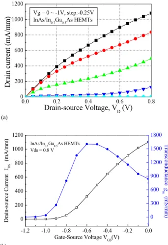
Fig. 2 (a) and 2 (b) shows the current-voltage characteristics of 2 × 50 μm devices of InAs/In0.53Ga0.47As composite channel HEMTs. As observed from the figure, this device can be well pinched off with a threshold voltage of -0.8 V. The fabricated InAs MHEMT shows a drain current density of 834 mA/mm and transconductance, gm,max of 1450 mS/mm at VDS = 0.8 V. On the other hand, the DC characteristics of the InAs/In0.7Ga0.3As composite channel
978-2-87487-007-1 © 2008 EuMA October 2008, Amsterdam, The Netherlands
Proceedings of the 3rd European Microwave Integrated Circuits Conference
HEMTs are shown in the Fig. 3 (a) and (b). The drain current density of 1101 mA/mm and gm,max of 1605 mS/mm are observed. The high transconductance was due to higher carrier concentration and superior electron transport properties in the InAs/In0.7Ga0.3As channel. The result indicates that the InAs-channel HEMTs can be operated at low drain bias condition to reduce dc power dissipation and is suitable for low power applications.
The S-parameters of the 2 × 50 μm device were measured from 5 to 80 GHz using on-wafer probing system with HP8510XF network analyzer. A standard Load-Reflection-Reflection-Match (LRRM) calibration method was used to calibrate the measurement system. The parasitic effects (mainly capacitive) due to the probing pads have been carefully removed from the measured S-parameters using the same method as in [11] and the equivalent circuit model in [12]. Fig. 4 shows the frequency dependence of the current gain H21, the power gain MAG/MSG, and the Mason’s unilateral gain U of the InAs/In0.53Ga0.47As device measured at VDS = 0.7 V and Vgs = -0.4 V. The fT and fmax are 310 and 330 GHz, respectively by extrapolating H21 and MAG/MSG by least square fitting with a -20 dB/dec slope. Comparison to the InAs/In0.7Ga0.3As channel device, a very high current gain cut-off frequency fT of 360 GHz and the maximum oscillation frequency fmax of 380 GHz were obtained and the results are shown in Fig. 5. The excellent RF performance of InAs/In0.7Ga0.3As composite channel device is mainly caused by high transconductance.
To characterize such device for high-speed logic applications, the gate delay time (CV/I) or intrinsic speed was also evaluated. C is the total gate capacitance including gate-to-source capacitance (Cgs) and gate-to-drain capacitance (Cgd) which extracted from the high frequency S-parameter. V is the applied drain voltage and equal to the power supply voltage (VCC). I is the on-state current with the bias point. According
to the definition in[13-14], the gate delay time of both devices
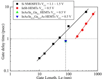
were calculated to be 0.87 (InAs/In0.53Ga0.47As) and 0.84 (InAs/In0.7Ga0.3As) psec at the same drain voltage VDS = 0.5 V, respectively. Fig. 6 shows the comparison of delay time for different types of devices (InAs HEMTs, advanced Si-MOSFETs and InSb HEMTs) as a function of gate length [2, 15]. In this plot, it can be seen that the 80 nm InAs HEMTs exhibits excellent intrinsic speed than the state-of-the-art Si NMOSFETs at the same gate length. It indicates the InAs is a material with great potential for low-voltage high-speed III-V-based logic circuit applications. Overall, the InAs/In0.7Ga0.3As HEMTs exhibit very well intrinsic speed, DC and RF performances owing to the appropriate epi-structure design, and short gate length.
IV. CONCLUSIONS
In this study, high performance 80 nm InAs/In1-xGaxAs composite-channel HEMTs with different indium content
sub-channel has been fabricated and characterized. The high
current gain cutoff frequency (fT) of 360 GHz and maximum
oscillation frequency (fmax) of 380 GHz were obtained at VDS
= 0.7 V with a calculated low gate delay time (0.84 psec at
VCC = 0.5 V) due to the high electron mobility in the
InAs/In0.7Ga0.3As channel. Overall, the device with In0.7Ga0.3As
sub-channel displays better characteristics than with In0.53Ga0.47As sub-channel because of the carrier confinement improvement and superior transport property. Finally, the device exhibits the sate-of-the-art performance and the device technology demonstrated is suitable for high-frequency milimeter wave and high-speed logic applications.
ACKNOWLEDGMENT
The authors would like to acknowledge the assistance and support from the National Science Council and the Ministry of Economic Affairs, Taiwan, R.O.C., under the contracts NSC 96-2752-E-009-001-PAE and 95-EC-17-A-05-S1-020. Part of this work was supported by the "Nanotechnology Support Project" of the Ministry of Education, Culture, Sports, Science and Technology (MEXT), Japan.
REFERENCES
[1] D. H. Kim, J. A. Alamo, J. H. Lee, and K. S. Seo, “Performance
Evaluation of 50 nm In0.7Ga0.3As HEMTs for beyond-CMOS logic
applications,” in IEDM Tech. Dig., 2005, pp.767-770.
[2] R. Chau, S. Datta, and A, Majumdar, “Opportunities and Chanllenges
of III-V Nanoelectronics for future high-speed,low-power logic applications,” in Proc. IEEE CSIC Dig., pp. 17-20, 2005.
[3] C. I. Kuo, H. T. Hsu, and E. Y. Chang, “InAs-Channel Based Quantum
Well Transistor,” Electrochemical and Solid-state Lett., 11 (7) pp. H193-H196 2008.
[4] Y. Yamashita, A. Endoh, K. Shinohra, K. Hikosaka, T. Matsui, S.
Hiyamizu, and T. Mimura, “Pseudomorphic In0.52Al0.48As/ In0.7Ga0.3As
HEMTs with an ultrahigh ft of 562 GHz,” IEEE Electron Device Lett.,
vol. 23, pp. 573-575, Oct. 2002.
[5] K. Shinohra, Y. Yamashita, A. Endoh, I. Watanabe, K. Hikosaka, T.
Matsui, T. Mimura, and S. Hiyamizu, “547 GHz ft In0.7Ga0.3As/
In0.52Al0.48As HEMTs With Reduced Source and Drain Resistance,”
IEEE Electron Device Lett., vol. 25, pp. 241-243, May 2004.
[6] S. J. Yeon, M. Park, J. Choi, and K. Seo, “610 GHz InAlAs/In0.75GaAs
Metamorphic HEMTs with an ultra-short 15-nm-gate,” in IEDM Tech.
Dig., pp.613-616 2007.
[7] T. Akazaki, K. Arai, T. Enoki, and Y. Ishii, “Improved InAlAs/InGaAs
HEMT Characteristics by Inserting an InAs Layer into the InGaAs Channel,” IEEE Electron Device Lett., vol. 13, pp. 325-327, June. 1992.
[8] G. Meneghesso, D. Buttari, E. Perin, C. Canali, and E. Zanoni,
“Improvement of DC, low frequency and reliability properties of InAlAs–InGaAs InP-based HEMTs by means of an InP etch stop layer,” in IEDM Tech. Dig., Dec. 1998, pp. 227–230.
[9] T. Suemitsu, H. Yokoyama, T. Ishii, T. Enoki, G. Meneghesso, and E.
Zanoni, “30-nm two-step recess gate InP-based InAlAs/InGaAs HEMTs,” IEEE Trans. Electron Devices, vol. 49, no. 10, pp. 1694– 1700, Oct. 2002.
[10] T. Suemitsu, H. Yokoyama, Y. Umeda, T. Enoki, and Y. Ishii, “High-performance 0.1-μm gate enhancement-mode InAlAs/InGaAs HEMTs using two-step recessed gate technology,” IEEE Trans. Electron
Devices, vol. 46, no. 6, pp. 1074-1080, Jun. 1999.
[11] Y. Yamashita, A. Endoh, K. Shinohara, M. Higashiwaki, K. Hikosaka, T. Mimura, S. Hiyamizu, and T. Matsui “Ultra-short 25nm Gate Lattice Match InAlAs/InGaAs HEMTs Within the Range of 400GHz Cut Off Frequency,” IEEE Electron Device Lett., vol. 22, pp. 367-369 August 2001
[12] G. Dambrine, A. Cappy, F. Heliodore, and E. Playez, “A new method for determining the FET small signal equivalent circuit,” IEEE Trans.
Microwave Theory Tech., vol. 36, pp.1151-1159, 1988
[13] R. Chau, S. Datta, M. Docyz, B. Doyle, B. Jin, J. Kavalieros, A. Majumdar, M. Metz, and M. Radosavljevic, “Benchmarking Nanotechnology for High-Performance and Low-Power Logic Transistor Applications”, IEEE Trans. Nanotechnology, Vol. 4, No. 2, pp. 153–158, 2005.
0.0 0.2 0.4 0.6 0.8 0 200 400 600 800 1000 D rai n current (m A /m m ) Drain-source Voltage, VDS (V) Vg = 0 ~ -0.8 V, step:-0.2 V InAs/In0.53Ga0.47As HEMTs -0.9 -0.6 -0.3 0.0 0 200 400 600 800 1000 for InAs/In0.53Ga0.47As VDS= 0.8 V Gate-Source Voltage VGS(V) D rain-source C urrent I DS ( m A /m m ) 0 500 1000 1500 2000 T rans conductance gm ( mS /mm) 0.0 0.2 0.4 0.6 0.8 0 200 400 600 800 1000 1200 Vg = 0 ~ -1V, step:-0.25V InAs/In0.7Ga0.3As HEMTs D rai n cur re nt (m A /m m ) Drain-source Voltage, VD (V) -1.2 -1.0 -0.8 -0.6 -0.4 -0.2 0.0 0 200 400 600 800 1000 1200 InAs/In0.7Ga0.3As HEMTs Vds = 0.8 V Gate-Source Voltage VGS(V) Drai n-so urc e C urr ent IDS (m A /m m ) 0 300 600 900 1200 1500 1800 T ransconductanc e g m (m S/m m ) 1 10 100 1000 0 10 20 30 40 50 60 Ug |h21|2 MAG/MSG Lg=80 nm Wg=2 x 50 µm VD= 0.7 V VG= - 0.4V fmax = 330 GHz ft= 310 GHz Ga in ( dB ) Frequency (GHz)
[14] J. Guo, A. Javey, H. Dai, and M. Lundstrom, “Performance analysis and design optimization of near ballistic carbon nano tube field effect transistors,” in IEDM Tech. Dig., 2004, pp.703-706.
[15] T. Ashley, A. R. Barnes, L. Buckle, S. Datta, A. B. Dean, M. T. Emeny, M. Fearn, D. G. Hayes, K. P. Hilton, R. Jefferies, T. Martin, K. J. Nash, T. J. Philips, W. H. A. Tang, and R. Chau, ‘‘InSb-based quantum well transistors for high speed, low power applications,’’ in Proc. CS-Mantech Conf., Apr. 2005.
Fig. 1 Cross-sectional SEM image of the 80nm T-shaped gate resist profile.
(a)
(b)
Fig. 2. Current-Voltage characteristics of the InAs/In0.53Ga0.47As 0.08 × 100
μm2 HEMTs. (a) Drain-source current versus drain-source voltage curves (b)
Transconductance versus gate-source voltage curves.
(a)
(b)
Fig. 3 Current-Voltage characteristics of InAs/In0.7Ga0.3As 0.08 × 100 μm2
HEMTs. (a) Drain-source current versus drain-source voltage curves (b) Transconductance versus gate-source voltage curves
Fig. 4 Typical current gain |h21|, MAG/MSG and Ug as a function of
frequency of a 0.08 μm × 100 μm InAs/In0.53Ga0.47As HEMT. The VDS is 0.7
V, and the VG is – 0.4 V.
1 10 100 1000 0 10 20 30 40 50 Lg=80 nm Wg=2x50 μm VD=0.7V VG=-0.5V MAG/MSG H21 U fmax=380 GHz ft=360 GHz Gai n ( dB) Frequency (GHZ) 1 10 100 1000 0.1 1 10 G ate d ela y tim e (psec) Gate Length, Lg (nm) Si NMOSFETs VCC = 1.1 ~ 1.5 V InSb HEMTs VCC = 0.5 V InAs/In0.7Ga0.3 HEMTs VCC = 0.5 V InAs/In0.53Ga0.47As HEMTs VCC = 0.5 V
Fig. 5 Frequency dependence of the current gain H21, the power gain
MAG/MSG, and the unilateral gain U of the InAs/In0.7Ga0.3As composite
channel HEMTs. The frequency range was from 5 to 80 GHz, and the device was biased at VDS = 0.7V and Vgs = -0.5V.
Fig. 6 Gate delay of InAs, InSb HEMTs and Si NMOSFETs as a function of gate length.