Growth of High-Aspect-Ratio Gold Nanowires on Silicon by
Surfactant-Assisted Galvanic Reductions
Ting-Kai Huang,
†Ying-Chieh Chen,
†Hsin-Chun Ko,
†Hsin-Wei Huang,
†Chia-Hsin Wang,
†Huang-Kai Lin,
†Fu-Rong Chen,
‡Ji-Jung Kai,
‡Chi-Young Lee,
§and Hsin-Tien Chiu*
,† Department of Applied Chemistry, National Chiao Tung UniVersity, Hsinchu, Taiwan 30050, Republic ofChina, and Department of Engineering and System Science and Center for Nanotechnology, Materials Science and Microsystems, National Tsing Hua UniVersity, Hsinchu, Taiwan 30043, Republic of China
ReceiVed January 8, 2008. ReVised Manuscript ReceiVed March 19, 2008
A simple galvanic reduction for direct growth of Au nanowires on silicon wafers is developed. The nanowires were prepared by reacting HAuCl4(aq)with Sn(s)in the presence of CTAC(aq)(cetyltrimethylammonium chloride) and NaNO3(aq), which were important to the product morphology development. The nanowire diameter was 50-100 nm, and the length was more than 20µm.
One-dimensional (1D) Au nanostructures, such as nanowires (NWs), nanorods (NRs), and nanobelts (NBs), have attracted considerable attention because they possess interesting shape-and size-dependent optical shape-and chemical properties shape-and can be applied to surface-enhanced Raman spectroscopy (SERS) and electrocatalysis.1–10 These can provide foundations to
new-generation devices for many applications. Murphy’s and El-Sayed’s groups have successfully developed multistep seed- and surfactant-mediated solution methods to synthesize Au NRs by reduction of HAuCl4(aq).1,11 Recently, the method has been
modified to raise the NR, with an aspect ratio of up to 25, in the product to exceed 90%.12,13There are also reports about growing
high-aspect-ratio NWs inside the channels of hard templates, such as anodic aluminum oxide (AAO) and polycarbonate by electrochemical deposition.14–19In the cases mentioned above, attaching the 1D nanostructures to substrates requires considerably more steps.1,14,20 On the other hand, Galvanic displacement reactions have been extensively used as efficient methods to grow novel nanostructures directly on substrates.21–28 For example, we recently demonstrated that Cu and Ag NBs can be grown by this way easily.28Here, we describe a simple method to grow high-density and high aspect ratio Au NWs directly on
Si surfaces by reducing HAuCl4(aq)with Sn(s)in the presence of
cetyltrimethylammonium chloride (CTAC) and NaNO3(aq).
A piece of Sn foil was pasted to the backside of a Si(100) wafer with a surface preroughed by an etching solution containing AgNO3(aq)and HF(aq). Then, the Sn-pasted Si was immersed into
a solution containing HAuCl4(aq), CTAC, and NaNO3(aq)at 303
K. After 72 h, growth of a golden layer on the Si surface was observed. Figure 1 shows typical field-emission scanning electron microscopic (FESEM) and energy dispersive spectroscopic (EDS) data of the as-prepared product on the Si. As displayed in Figure
* Corresponding author. E-mail: [email protected].
†National Chiao Tung University.
‡Department of Engineering and System Science, National Tsing Hua
University.
§Center for Nanotechnology, Materials Science and Microsystems,
National Tsing Hua University.
(1) Murphy, C. J.; Sau, T. K.; Gole, A. M.; Orendorff, C. J.; Gao, J.; Gou, L.; Hunyadi, S. E.; Li, T. J. Phys. Chem. B 2005, 109, 13857.
(2) Xu, Q.; Bao, J.; Capasso, F.; Whitesides, G. M. Angew. Chem., Int. Ed. 2006, 45, 3631.
(3) Nikoobakht, B.; El-Sayed, M. A. J. Phys. Chem. A 2003, 107, 3372. (4) Nikoobakht, B.; Wang, J.; El-Sayed, M. A. Chem. Phys. Lett. 2002, 366, 17.
(5) Grand, J.; de la Chapelle, M. L.; Bijeon, J.-L.; Adam, P.-M.; Vial, A.; Royer, P. Phys. ReV. B 2005, 72, 033407.
(6) Billot, L.; de la Chapelle, M. L.; Grimault, A.-S.; Vial, A.; Barchiesi, D.; Bijeon, J.-L.; Adam, P.-M.; Royer, P. Chem. Phys. Lett. 2006, 422, 303.
(7) Lapierre-Devlin, M. A.; Asher, C. L.; Taft, B. J.; Gasparac, R.; Roberts, M. A.; Kelley, S. O. Nano Lett. 2005, 5, 1051.
(8) Hernandez, J.; Solla-Gullon, J.; Herrero, E.; Aldaz, A.; Feliu, J. M. Phys. Chem. B 2005, 109, 12651.
(9) Zhang, J.; Du, J.; Han, B.; Liu, Z.; Jiang, T.; Zhang, Z. Angew. Chem., Int. Ed. 2006, 45, 1116.
(10) Chen, Y.; Milenkovic, S.; Hassel, A. W. Nano Lett. 2008, 8, 737. (11) Nikoobakht, B.; El-Sayed, M. A. Chem. Mater. 2003, 15, 1957. (12) Wu, H.-Y.; Chu, H.-C.; Kuo, T.-J.; Kuo, C.-L.; Huang, M. H. Chem. Mater. 2005, 17, 6447.
(13) Wu, H.-Y.; Huang, W.-L.; Huang, M. H. Cryst. Growth Des. 2007, 7, 831.
(14) Choi, J.; Sauer, G.; Go¨ring, P.; Nielsch, K.; Wehrspohna, R. B.; Go¨sele, U. J. Mater. Chem. 2003, 13, 1100.
(15) Liu, J.; Duan, J. L.; Toimil-Molares, M. E.; Karim, S.; Cornelius, T. W.; Dobrev, D.; Yao, H. J.; Sun, Y. M.; Hou, M. D.; Mo, D.; Wang, Z. G.; Neumann, R. Nanotechnology 2006, 17, 1922.
(16) Choi, J.; Sauer, G.; Nielsch, K.; Wehrspohn, R. B.; Gosele, U. Chem. Mater. 2003, 15, 776.
(17) Wang, J.-G.; Tian, M.-L.; Mallouk, T. E.; Chan, M. H. W. J. Phys. Chem. B 2004, 108, 841.
(18) Tian, M.-L.; Wang, J.-G.; Kurtz, J.; Mallouk, T. E.; Chan, M. H. W. Nano Lett. 2003, 3, 919.
(19) Zhang, J.; Wang, X.; Peng, X.; Zhang, L. Appl. Phys. A: Mater. Sci. Process. 2002, 75, 485.
(20) Yoo, S.-H.; Park, S. AdV. Mater. 2007, 19, 1612.
(21) Aizawa, M.; Cooper, A. M.; Malac, M.; Buriak, J. M. Nano Lett. 2005, 5, 815.
(22) Qu, L.; Dai, L. J. Am. Chem. Soc. 2005, 127, 10806. (23) Qu, L.; Dai, L.; Osawa, E. J. Am. Chem. Soc. 2006, 128, 5523. (24) Sun, Y. G.; Mayers, B. T.; Xia, Y.-N. Nano Lett. 2002, 2, 481. (25) Sun, Y. G.; Mayers, B. T.; Xia, Y.-N. AdV. Mater. 2003, 15, 641. (26) Chen, J.; McLellan, J. M.; Siekkinen, A.; Xiong, Y.; Li, Z.-Y.; Xia, Y.-N. J. Am. Chem. Soc. 2006, 128, 14776.
(27) Yang, J.; Griffiths, P. R. Anal. Bioanal. Chem. 2007, 388, 109. (28) Huang, T.-K.; Cheng, T.-H.; Yen, M.-Y.; Hsiao, W.-H.; Wang, L.-S.; Chen, F.-R.; Kai, J.-J.; Lee, C.-Y.; Chiu, H.-T. Langmuir 2007, 23, 5722.
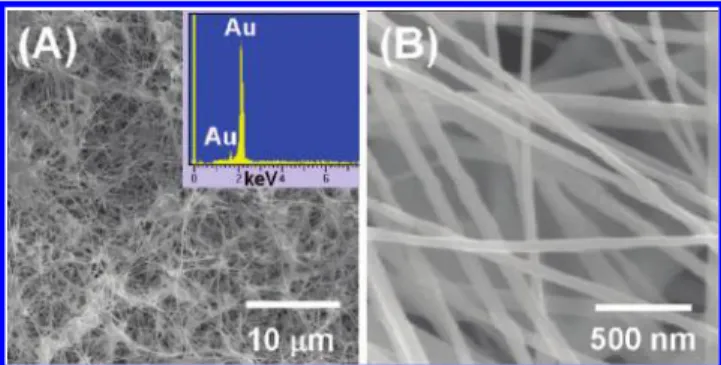
Figure 1.SEM images of Au NWs grown on preroughened Si: (A) low magnification (inset: EDS) and (B) high magnification.
5647
Langmuir 2008, 24, 5647-5649
10.1021/la8000575 CCC: $40.75 2008 American Chemical Society Published on Web 04/29/2008
1A, 1D nanostructures, tens of micrometers in length, grow densely to cover the entire surface. The EDS (inset) confirms that the product is composed of Au only. Figure 1B shows an enlarged view of the product, suggesting it contains NWs with diameters of 50-100 nm. The estimated aspect ratio is more than 200. In addition to the NWs, other shapes, such as spherical nanoparticles (NPs) and triangular and hexagonal nanosheets (NSs), are observed in minor quantities. X-ray diffraction (XRD) studies confirmed that face-centered cubic (fcc) Au was deposited on the Si substrates.
Figure 2 shows transmission electron microscopic (TEM) studies of representative NWs. We have discovered that the sample contained NWs grown into two typical structures. As shown in Figure 2A, a straight NW feature is consistent with the SEM observation. In Figure 2B, a selected area electron diffraction (SAED), from a rectangular region marked in Figure 2A, shows a composite reflection pattern. It corresponds to the superposition of [-111] and [110] crystallographic zones of an fcc structure, indicating that the NW is not single crystalline. This is similar to the pattern of a penta-twinned Au NR commonly observed in literature.29–31For the NW in Figure 2A, the growth direction is indexed to be along [110]. The lattice parameter a is calculated to be 0.40 nm, in good agreement with the reported value of Au, 0.4079 nm (JCPDS 89-3697). A high-resolution TEM (HRTEM) image in Figure 2C shows a d-spacing of 0.203 nm, which is close to that of Au {200} planes, 0.2039 nm. Detailed studies
of the crystal structure, with the sample stage in positions normal and tilted 18°along the longitudinal axis of the NW, have been done by SAED and dark-field TEM techniques (see Supporting Information). The result is consistent with the penta-twinned NW crystal structures. Normally, the NW structures contain 10 {111} end faces, 5 {100} side faces, elongated along the [110] direction, and a pentagon-shaped cross section.32–35In addition
to the penta-twinned NW structure, there is another type of NW in the sample. Figure 2D shows a NW image that is essentially the same as the one shown in Figure 2A. However, in Figure 2E, the SAED of this NW displays a simple square diffraction pattern of an fcc structure along the [001] crystallographic zone. This contrasts the composite pattern observed in Figure 2B. The lattice parameter a is also calculated to be 0.40 nm, which is close to the value of Au. This suggests that the NW is single crystalline and grows along the direction of [110]. Throughout the NW, the HRTEM image shows two orthogonal fringes, as displayed in Figure 2C. The d-spacing measured from the image is 0.204 nm. This is close to the reported value of Au {200} planes. After eight samples were examined by TEM, the ratio of the twined/ single crystalline NWs is found to be 4:4. This suggests that the sample contains a roughly equivalent amount of two types of NWs. The reason for the development of NWs into different structures may lie in the early nucleation stage differences.
As suggested by the following equation, 2 AuCl4-(aq)+ 3 Sn(s)
f2 Au(s) + 3 Sn2+(aq)+ 8Cl-(aq), E°) 1.142 V, the overall reduction of AuCl4-(aq)by Sn(s)to form Au NWs is
thermody-namically favored.36However, thermodynamics alone cannot
explain why Au would grow into NWs under the conditions employed. We found that the Si surface preroughen step is important. Without it, both reduction of AuCl4-(aq) ions and
nucleation of Au(s)appear to be difficult on a perfectly flat Si
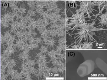
surface. We speculate the etching step not only removes the surface oxide layer but also creates surface defects to assist the Au nucleation. To investigate the growth process of Au NWs at the early stage, the image of a sample at 18 h is shown in Figure 3. The low-magnification SEM image in Figure 3A shows the presence of urchin-like particles with multiple needles on Si. A detailed view in Figure 3B suggests that the needles have diameters of 100-140 nm and lengths of 1-5µm. Apparently, as shown in Figure 3B, the protruding needles are on top of an aggregate of particles, which may act as the NW nucleation sites. Although multiple-pod Au particles have been synthesized in homogeneous solution before, this is the first observation of Au needles growing outward from fixed sites on a surface.37
Figure 3C shows a short Au NR displaying an apparent pentagonal cross-section at its early growth stage. This agrees well with the penta-twinned NW structure characterized by TEM studies in Figures 2A-C.
We discover that growing Au NWs required a combination of right HAuCl4(aq), CTAC, and NaNO3(aq) concentrations, a (29) Johnson, C. J.; Dujardin, E.; Davis, S. A.; Murphy, C. J.; Mann, S. J. Mater. Chem. 2002, 12, 1765.
(30) Elechiguerra, J. L.; Reyes-Gasgab, J.; Yacaman, M. J. J. Mater. Chem. 2006, 16, 3906.
(31) Lisiecki, I.; Filankembo, A.; Sack-Kongehl, H.; Weiss, K.; Pileni, M.-P.; Urban, J. Phys. ReV. B 2000, 61, 4968.
(32) Sun, Y. G.; Mayers, B.; Herricks, T.; Xia, Y.-N. Nano Lett. 2003, 3, 955. (33) Gao, Y.; Jiang, P.; Liu, D. F.; Yuan, H. J.; Yan, X. Q.; Zhou, Z. P.; Wang, J. X.; Song, L.; Liu, L. F.; Zhou, W. Y.; Wang, G.; Wang, C. Y.; Xie, S. S.; Zhang, J. M.; Shen, D. Y. J. Phys. Chem. B 2004, 108, 12877.
(34) Reyes-Gasgaa, J.; Elechiguerraa, J. L.; Liub, C.; Camacho-Bragadob, A.; Montejano-Carrizalesc, J. M.; Jose Yacamana, M. J. Cryst. Growth 2006, 286, 162.
(35) Zhang, S.-H.; Jiang, Z.-Y.; Xie, Z.-X.; Xu, X.; Huang, R.-B.; Zheng, L.-S. J. Phys. Chem. B 2005, 109, 9416.
(36) Bard, A. J.; Faulkner, L. R. Electrochemical Methods: Fundamentals and Applications; John Wiley & Sons: New York, 1980.
(37) Kuo, C.-H.; Huang, M. H. Langmuir 2005, 21, 2012.
Figure 2.TEM studies of Au NWs. (A) Low-magnification TEM of Au NWs, (B) SAED of the long NW in panel A showing superposition of [-111] and [110] zones, (C) HRTEM of the rectangular region in panel A, (D) low-magnification TEM of another Au NW, (E) [001] zone SAED, and (F) HRTEM of the rectangular region in panel E.
properly treated substrate, and an accurately controlled reaction temperature. Without them, the Au NWs could not grow. Instead, other morphologies, such as NSs and NPs, were observed. It is well-known that surfactants, such as cetyltrimethylammonium bromide (CTAB), can act as growth control agents to assist the elongation of Au NPs into NRs and NWs.1,13In this investigation,
we discover that when only NaNO3(aq)but no CTAC was added,
a nanothorn (NT) type of morphology was developed on Si (see Supporting Information). The typical NTs showed heights of several micrometers. Their cross-sections were polygon shaped, and the base widths were hundreds of nanometers. The SAED study of a representative NT sample displayed a composite pattern that originated from a twinned fcc Au structure with [110] growth direction. On the basis of this result and the data showed in Figure 2, we suggest that the NO3-(aq)ions may inhibit the growth
of Au faces in multiple dimensions so that the deposition of Au atoms on Au (220) becomes a preferred direction. We also discovered that by adding only CTAC but without a suitable amount of NaNO3(aq), Au NWs could not grow on the
pre-roughened Si surface. Nonetheless, we also found that, on a Sn-pasted carbon paste electrode, Au NWs could be grown with the assistance of CTAC only, without the addition of NaNO3(aq).
In this case, the NW was not the only product. Au NPs and NSs were deposited as well. Many studies reported that, in addition to the presence of a surfactant as the growth control agent, the addition of NO3-(aq)ions appeared to be another essential factor
for the development of 1D nanostructures.12,13,28,38
A generalized CTAC-assisted Au NW growth process is presented in Scheme 1. The reaction is a galvanic reduction of AuCl4-(aq)by more active Sn(s)into Au(s). The AuCl4-(aq)ions
are reduced by the electrons released from the oxidized Sn(s)to
deposit Au atoms on Si. By diffusion, these unstable Au atoms diffuse and coalesce on the surface to form Au clusters. The clusters enlarge as more Au atoms are deposited. The role of NO3-(aq)ions in the reaction may resemble their function in aqua
regia, which is well-known for its ability to oxidize Au(s)into
AuCl4-(aq)ions.39We assume that some of the Au(s)crystal faces
may be oxidized more easily than the others. This may result in Au(s)NPs with preferred orientation. This is supported by the
NTs discussed above. As suitable Au nanocrystalline seeds, such as NTs, are formed, the CTAC molecules probably adsorb selectively on preferred low-index facets, such as {111} and
{200}.40,41We speculate that the surfactant molecules form a
bilayer interface between the growing Au(s) crystal and the
solution. This specific arrangement restricts the deposition of Au atoms on the CTAC passivated facets. Consequently, the Au crystal can only grow along the [110] direction into a NW. This is comparable to many recent reports, which discuss the growth of fcc phase metals Cu, Ag, Au, and Pb into 1D nanostructures with [110] growth direction under the influence of surfactants as the surface capping agents.35,42–45
The electrical resistivity of an Au NW with a diameter of 92 nm was derived from its I-V property obtained by the two-point probe method. The calculated value is 3.7× 10⁻⁷Ω m, which is about an order higher than the reported values of a Au NW (250 nm in diameter) and the bulk Au(s), 2.2× 10⁻⁸and 8×
10-8Ωm, respectively.46The higher resistivity of the Au NW
studied here may be attributed to a combination of the presence of crystal defects and the imperfect contacts between the NW and the probes. The presence of the CTAC bilayer may hamper the electron flow and raise the resistance.
In conclusion, we have discovered a simple method which combines the growth and immobilization of high-aspect-ratio Au NWs in large scale on Si in a simple step. The reaction is a galvanic reduction of HAuCl4(aq)by Sn(s)attached to the substrate
in the presence of CTAC(aq)and NaNO3(aq). Both CTAC molecules
and NO3- ions are essential ingredients to shape the highly
symmetric fcc Au crystals into the 1D morphology. We expect that the Au NWs will have high potentials in electrochemical devices and SERS studies.
Acknowledgment. We thank the National Science Council and
the Ministry of Education of Taiwan, the Republic of China, for financial support. We also appreciate Prof. Jyisy Yang and Miss. Min-Liang Cheng (NCHU) for their assistance on SERS studies and Mr. I-Chun Chang (NCTU) for the experimental help.
Supporting Information Available:Experimental procedures, photographic image, XRD, TEM, ED, SEM, I-V profile, and SERS data. This material is available free of charge via the Internet at http://pubs.acs.org.
LA8000575
(38) Herricks, T.; Chen, J.; Xia, Y. Nano Lett. 2004, 4, 2367.
(39) Greenwood, N. N.; Earnshaw, A. Chemistry of The Elements; Elsevier Science: Boston, 1997.
(40) Gao, J.; Bender, C. M.; Murphy, C. J. Langmuir 2003, 19, 9065. (41) Nikoobakht, B.; El-Sayed, M. A. Langmuir 2001, 17, 6368. (42) Zhang, D. B.; Qi, L. M.; Yang, J. H.; Ma, J. M.; Cheng, H. M.; Huang; L, Chem. Mater. 2004, 16, 872.
(43) Hu, J. Q.; Chen, Q.; Xie, Z. X.; Han, G. B.; Wang, R. H.; Ren, B.; Zhang, Y.; Yang, Z. L.; Tian, Z. Q. AdV. Funct. Mater. 2004, 14, 183.
(44) Chen, J.-Y.; Wiley, B. J.; Xia, Y.-N. Langmuir 2007, 23, 4120. (45) Chang, Y.; Lye, M.-L.; Zeng, H.-C. Langmuir 2005, 21, 3746. (46) Liu, S.; Tok, J. B.-H.; Bao, Z. Nano Lett. 2005, 5, 1071.
Figure 3.SEM images of urchin-like Au morphology grown on Si for 18 h: (A) low-magnification, (B) high magnification, and (C) a short NR on the substrate.
Scheme 1.Proposed Growth Mechanism of Au NWs on Si