Strain relaxation and induced defects in InAsSb self-assembled quantum dots
J. F. Chen, R. S. Hsiao, W. D. Huang, Y. H. Wu, L. Chang, J. S. Wang, and J. Y. Chi
Citation: Applied Physics Letters 88, 233113 (2006); doi: 10.1063/1.2212064 View online: http://dx.doi.org/10.1063/1.2212064
View Table of Contents: http://scitation.aip.org/content/aip/journal/apl/88/23?ver=pdfcov Published by the AIP Publishing
Articles you may be interested in
Strain relaxation and phonon confinement in self-assembled InAsSb/InP (001) quantum dashes: Effect of deposition thickness and composition
Appl. Phys. Lett. 97, 223108 (2010); 10.1063/1.3522889
Strain relaxation in InAs self-assembled quantum dots induced by a high N incorporation J. Appl. Phys. 104, 103717 (2008); 10.1063/1.3028235
Strain status of self-assembled InAs quantum dots Appl. Phys. Lett. 77, 1295 (2000); 10.1063/1.1290152
Strain relaxation and segregation effects during self-assembled InAs quantum dots formation on GaAs(001) Appl. Phys. Lett. 77, 409 (2000); 10.1063/1.126992
Strain relaxation-induced modifications of the optical properties of self-assembled InAs quantum dot superlattices J. Vac. Sci. Technol. B 18, 1493 (2000); 10.1116/1.591411
This article is copyrighted as indicated in the article. Reuse of AIP content is subject to the terms at: http://scitation.aip.org/termsconditions. Downloaded to IP: 140.113.38.11 On: Thu, 01 May 2014 01:57:30
Strain relaxation and induced defects in InAsSb self-assembled
quantum dots
J. F. Chen,a兲 R. S. Hsiao, and W. D. Huang
Department of Electrophysics, National Chiao Tung University, Hsinchu 30050, Taiwan, Republic of China Y. H. Wu and L. Chang
Department of Materials Science and Engineering, National Chiao Tung University, Hsinchu 30050, Taiwan, Republic of China
J. S. Wang
Department of Physics, Chung Yuan Christian University, Chung-Li 32023, Taiwan, Republic of China J. Y. Chi
Industrial Technology Research Institute (OES/ITRI), Hsinchu 310 Taiwan, Republic of China 共Received 20 January 2006; accepted 15 May 2006; published online 8 June 2006兲
The onset of strain relaxation and induced defects in InAs0.94Sb0.06quantum dots are investigated.
We show that the relaxation causes partial carrier depletion in the dots and drastic carrier depletion in the top GaAs layer due to the introduction of two defect traps at 0.35 and 0.64 eV. This result is consistent with transmission electron microscopy data which show misfit dislocations on the edges of the dot upper boundary and threading dislocations in the top GaAs layer. The bottom GaAs layer is dislocation-free, and thus the strain relaxation may initially occur on the edges of the dots. © 2006 American Institute of Physics.关DOI:10.1063/1.2212064兴
Self-assembled InAs quantum dots1–5共QDs兲 are of great interest for practical applications and scientific studies. Such dots are usually formed by Stranski-Krastanow growth. When depositing the InAs layer to about 1.7 ML 共monolayer兲,2–4
strain is partially relieved by forming the dots coherently. To extend the emission wavelength, it is necessary to increase the dot size by increasing the InAs thickness.6 However, when the InAs thickness reaches a critical thickness7共about 3 ML兲, strain is further relaxed by introduction of misfit dislocations. This strain relaxation is more complicated than in a planar system and may be af-fected by the incorporation of isoelectronic dopants. The in-troduction of antimony共Sb兲 as a surfactant8,9into a strained InGaAs quantum well共QW兲 has been shown to delay three-dimensional 共3D兲 growth and thus extend the emission wavelength. Recently, dilute Sb has been incorporated into InAs QDs 共Ref. 10兲 and an emission at 1.3m at room temperature has been demonstrated.11 Despite these efforts, however, the properties of strain relaxation in InAsSb QDs have never been characterized. Thus, in this letter, we report our studies of the strain relaxation in InAsSb QDs by per-forming capacitance-voltage 共C-V兲, transmission electron microscopy 共TEM兲, and deep-level transient spectroscopy 共DLTS兲 measurements.
InAsSb QDs were grown on n+-GaAs 共100兲 substrates by molecular beam epitaxy in a Riber Epineat machine. The QDs were formed in Stranski-Krastanow growth mode by depositing the InAsSb layer at 485 ° C and a growth rate of 0.256 Å / s. A conventional Sb K cell was set at 305 ° C to provide a beam flux of 3.5⫻10−7torr, which corresponds to
6% Sb composition estimated from the x-ray data of GaAsSb layers. Reflection high-energy electron diffraction共RHEED兲 patterns showed a transition to spotty after⬃25 s growth of the InAsSb layer, in comparison to⬃20 s for the QDs
with-out Sb, indicating a retarded QD formation by the Sb incorporation.10For electrical characterizations, the QDs are sandwiched between two 0.3-m-thick Si-doped GaAs 共6⫻1016cm−3兲 layers. Detailed growth of the QDs can be
found elsewhere.12 Schottky diodes were realized by evapo-rating Al on the sample with a dot diameter of 1500m.
Figure 1 shows the 20 K carrier distributions converted from the C-V spectra of the InAs0.94Sb0.06QDs Schottky
di-odes with 2-, 2.2-, and 2.8-ML-thick InAsSb layers. The 2 and 2.2 ML samples show a strong carrier-accumulation peak at the dots. Both peaks show no frequency-dependent attenuation, reflecting a very fast electron emission for quan-tum states. The peak linewidth of the 2.2 ML sample is much narrower than that of the 2 ML sample due to improved size uniformity for larger dots, as indicated by
photolumines-a兲Electronic mail: [email protected]
FIG. 1. Carrier distributions at 20 K of the InAsSb QDs samples with 2-, 2.2-, and 2.8-ML-thick InAsSb layers. The 2 and 2.2 ML samples show strong carrier accumulation at the dots but the 2.8 ML sample exhibits weak accumulation at the dots and drastic carrier depletion in the top GaAs layer.
APPLIED PHYSICS LETTERS 88, 233113共2006兲
0003-6951/2006/88共23兲/233113/3/$23.00 88, 233113-1 © 2006 American Institute of Physics
This article is copyrighted as indicated in the article. Reuse of AIP content is subject to the terms at: http://scitation.aip.org/termsconditions. Downloaded to IP: 140.113.38.11 On: Thu, 01 May 2014 01:57:30
cence 共PL兲 spectra which show a redshift of 300 K QD ground-state emission from 1235 to 1255 nm and decreased linewidth as increasing the InAsSb thickness from 2 to 2.2 ML. In contrast, the 2.8 ML sample exhibits weak accumu-lation at the dots共at 0.28m兲 and drastic carrier depletion 共at around 0.23m兲 in the top GaAs layer. This sudden deg-radation is accompanied with a broadening of a PL emission at 1285 nm and can be attributed to strain relaxation by in-troduction of carrier-depletion traps. As consistent with the normal carrier distribution in the bottom GaAs layer, the weak accumulation peak at the dots shows no frequency-dependent attenuation, suggesting that no traps are induced in the neighboring GaAs bottom layer, since any traps there would considerably increase the emission time.13 Accord-ingly, the critical thickness for defect introduction should be between 2.2 and 2.8 ML, a value slightly smaller than those 共between 2.7 and 3.06 ML兲 previously obtained in InAs QDs,6,13 probably due to an increased lattice mismatch due to the Sb incorporation.
The normal carrier distributions in the 2 and 2.2 ML samples are consistent with their TEM data, where no appar-ent dislocations were observed. On the other hand, the
cross-sectional TEM picture of the 2.8 ML sample, as shown in Fig. 2共a兲, shows threading dislocations in the top GaAs layer. Traps associated with these threading dislocations can be re-sponsible for the drastic carrier depletion in the top GaAs layer. Figure 2共b兲 shows the high resolution TEM 共HRTEM兲 picture of a typical dot共dashed ellipse兲 which is the one at the right-hand side in the inset of the figure. This dot has a height of ⬃5 nm and a width of ⬃20 nm. To see lattice misfits, Fig. 2共c兲 shows the corresponding Fourier trans-formed image. A total of eight misfits with two in each of the two large circles at the right-hand side and one in each of the rest circles can be seen. Among them, six are on the edges of the QD upper boundary and two are inside the dot. For a dot density of⬃3⫻1010cm−2observed by atomic force micros-copy 共AFM兲, the average density of the misfits is ⬃2.4⫻1011cm−2. Defects associated with these misfits can
trap electrons and explain the partially carrier depletion in the dots. Note that the bottom GaAs layer is dislocation-free and thus the dot lower interface likely remains coherently strained. From the spatial distribution of these misfits, we deduce that the strain relaxation initially occurs at the edges of the dot upper boundary where considerable stress may be accumulated or inhomogeneities or threading dislocations are probably produced for providing nucleation sources for misfit dislocations.
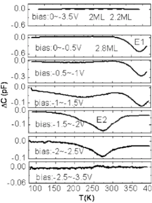
The relaxation-induced traps were revealed by the DLTS spectra shown in Fig. 3. As shown in the top figure, the 2 and 2.2 ML samples, measured by sweeping from 0 to − 3.5 V, exhibit no traps, indicating a coherent formation of the QDs. In contrast, the 2.8 ML sample exhibits a trap E1in the
top GaAs layer and a trap E2 near the dots. No traps are visible in the GaAs bottom layer. Arrhenius plots yield an activation energy 共capture cross section兲 of 0.64 eV 共2.11⫻10−15cm−2兲 for the E
1 trap and 0.35 eV
共1.18⫻10−17cm−2兲 for the E
2 trap. As filling pulse width
increases, the intensity of the E1trap continuously increases
without saturation. Figure 4共a兲 shows that its 300 K transient response, measured after sweeping from 0 to − 0.5 V, can be fitted by a logarithmic function 共open squares兲. This signa-FIG. 2. Cross-sectional TEM picture of the 2.8 ML sample, illustrating a
line of dots and threading dislocations in the top GaAs layer. 共b兲 The HRTEM picture of a dot共dashed ellipse兲, corresponding to the one at the right-hand side in the inset.共c兲 The corresponding Fourier transformed im-age, showing two misfits in each of the two large circles at the right-hand side and one misfit in each of the rest.
FIG. 3. DLTS spectra of the studied samples. The 2 and 2.2 ML samples exhibit no traps due to a coherent formation of the QDs but the 2.8 ML sample exhibits a trap E1in the GaAs top layer and a trap E2near the dots.
No traps are visible in the GaAs bottom layer.
233113-2 Chen et al. Appl. Phys. Lett. 88, 233113共2006兲
This article is copyrighted as indicated in the article. Reuse of AIP content is subject to the terms at: http://scitation.aip.org/termsconditions. Downloaded to IP: 140.113.38.11 On: Thu, 01 May 2014 01:57:30
ture is characteristic of Coulombic repulsion of the carriers captured at the traps along the linearly arrayed dislocation lines,14and thus confirms that the E1 trap is associated with
the threading dislocations in the top GaAs layer. On the other hand, the intensity of the E2 trap is found to saturate at ⌬C=0.125 pF with filling pulse width. From this saturated intensity, a sheet density is obtained to be 109cm−2 from NT= ND共⌬C/C02兲A where ND= 6⫻1016cm−3, C0= 220 pF,
area A = 5⫻10−3 cm2, and permittivity=1.14⫻10−10F / m.
This concentration is about two orders of magnitude less than that of the misfits estimated from the TEM data, and thus the E2trap is unlikely associated with the localized state
due to the destruction of lattice translational symmetry by misfit dislocations. Figure 4共b兲 shows that its transient re-sponse, by sweeping from −2 to − 2.5 V, except at the very initial time, can be fitted by an exponential function. This signature suggests that the E2 trap may be isolated point defects associated with misfit dislocations. By comparison, these two traps are believed to be the E1and E5traps
previ-ously observed in relaxed InAs QDs,7indicating that they are common relaxation-induced traps and are independent of Sb incorporation. The other three traps observed in Ref. 7 are not detected in this study. Since isoelectronic dopants have been shown to reduce the dislocation density15or inhibit the motion of dislocations,16 we suspect that the Sb incorpora-tion may play a role of preventing the occurrence of these traps. Detailed studies are underway in this direction.
The authors would like to thank the National Science Council of Taiwan, Republic of China for financially supporting this research under Contract No. NSC-94-2112-M-009-029.
1F. Heinrichsdorff, M.-H. Mao, N. Kirstaedter, A. Krost, and D. Bimberg,
Appl. Phys. Lett. 71, 22共1997兲.
2D. J. Eaglesham and M. Cerullo, Phys. Rev. Lett. 64, 1943共1990兲. 3S. Guha, A. Madhukar, and K. C. Rajkumar, Appl. Phys. Lett. 57, 2110
共1990兲.
4C. W. Snyder, J. F. Mansfield, and B. G. Orr, Phys. Rev. B 46, 9551
共1992兲.
5Y. Arakawa and H. Sakaki, Appl. Phys. Lett. 40, 939共1982兲.
6J. F. Chen, R. S. Hsiao, Y. P. Chen, J. S. Wang, and J. Y. Chi, Appl. Phys.
Lett. 87, 141911共2005兲.
7J. S. Wang, J. F. Chen, J. L. Huang, P. Y. Wang, and X. J. Guo, Appl. Phys.
Lett. 77, 3027共2000兲.
8X. Yang, M. J. Jurlovic, J. B. Heroux, and W. I. Wang, Appl. Phys. Lett. 75, 178共1999兲.
9J. C. Harmand, L. H. Li, G. Patriarche, and L. Travers, Appl. Phys. Lett. 84, 3981共2004兲.
10T. Matsuura, T. Miyamoto, T. Kageyama, M. Ohta, Y. Matsui, T. Furuhata,
and F. Koyama, Jpn. J. Appl. Phys., Part 2 43, L605共2004兲.
11K. Suzuki and Y. Arakwa, Phys. Status Solidi B 224, 139共2001兲. 12J. F. Chen, R. S. Hsiao, S. H. Shih, P. Y. Wang, J. S. Wang, and J. Y. Chi,
Jpn. J. Appl. Phys., Part 2 43, L1150共2004兲.
13J. F. Chen, R. S. Hsiao, C. K. Wang, J. S. Wang, and J. Y. Chi, J. Appl.
Phys. 98, 013716共2005兲.
14T. Wosinski, J. Appl. Phys. 65, 1566共1989兲.
15H. Beneking, P. Narozny, and N. Emeis, Appl. Phys. Lett. 47, 828共1985兲. 16P. A. Kirkby, IEEE J. Quantum Electron. QE11, 562共1975兲.
FIG. 4.共a兲 Transient response of the E1trap, measured after sweeping from
0 to − 0.5 V. This response can be fitted by a logarithmic function共open squares兲. 共b兲 Transient response of the E2 trap, measured after sweeping
from −2 to − 2.5 V, which, except at the very initial time, can be fitted by an exponential function.
233113-3 Chen et al. Appl. Phys. Lett. 88, 233113共2006兲
This article is copyrighted as indicated in the article. Reuse of AIP content is subject to the terms at: http://scitation.aip.org/termsconditions. Downloaded to IP: 140.113.38.11 On: Thu, 01 May 2014 01:57:30