國 立 交 通 大 學
電子工程學系 電子研究所碩士班
碩 士 論 文
氧化銦錫擴散電流層厚度對氮化鎵發光二極體光電特
性的影響
Influence on Optical and Electrical Characteristics of
GaN-based Light-emitting Diodes by Varying the
Thickness of Indium-tin-oxide Current Spreading Layers
研 究 生 : 郭 端 祥
指導教授 : 張 國 明 博士
桂 正 楣 博士
氧化銦錫擴散電流層厚度對氮化鎵發光二極體光電特性的
影響
Influence on Optical and Electrical Characteristics of
GaN-based Light-emitting Diodes by Varying the Thickness of
Indium-tin-oxide Current Spreading Layers
研 究 生:郭端祥 Student:Duan-Hsiang Guo
指導教授:張國明 博士 Advisor:Dr. Kow-Ming Chang
桂正楣 博士 Dr. Cheng-May Kwei
國 立 交 通 大 學
電子工程學系 電子研究所碩士班
碩 士 論 文
A Thesis
Submitted to Institute of Electronics
College of Electrical Engineering and Computer Science
National Chiao Tung University
In Partial Fulfillment of the Requirements
for the Degree of
Master
In
Electronics Engineering
June 2005, Hsinchu, Taiwan, Republic of China
氧化銦錫擴散電流層厚度對氮化鎵發光二極體光電特
性的影響
研究生:郭端祥
指導教授:張國明 博士
桂正楣 博士
國立交通大學
電子工程學系 電子研究所碩士班
摘
要
近年來,隨著氮化鎵發光二極體的發展,高透明度且電阻率小的氧化銦錫已 經被廣泛的用作為透明電流擴散層。在此篇研究中,於 P 型氮化鎵上蒸鍍了不同 厚度的氧化銦錫薄膜,並且製造成傳統的發光二極體,用以研究氧化銦錫薄膜和 發光二極體元件的光電特性。我們發現氧化銦錫薄膜的片電阻值會隨著其厚度增 加而降低,並影響到電流擴散能力和動態串接電阻值,氧化銦錫晶粒尺寸也和其 厚度有關。另外,接觸電阻係數也受到在氧化銦錫和氮化鎵界面間氧含量的支 配。然而,電流擴散長度或氧化銦錫厚度似乎都和量測到的元件亮度沒有關連, 我們嘗試找出造成此種不一致的可能原因。Influence on Optical and Electrical Characteristics of
GaN-based Light-emitting Diodes by Varying the
Thickness of Indium-tin-oxide Current Spreading Layers
Student:Duan-Hsiang Guo Advisor:Dr. Kow-Ming Chang
Dr. Cheng-May Kwei
Institute of Electronics
National Chiao Tung University
ABSTRACT
With the development of nitride-based light-emitting diodes (LEDs) in the past year, indium-tin-oxide (ITO) has been widely applied as a transparent current spreading layer due to its high transparency and low electrical resistivity. In this research, ITO films with different thicknesses are evaporated on p-type GaN, and then the conventional GaN-based LEDs are fabricated. Optical and electrical characteristics of these ITO films and LED devices have been analyzed. We find that sheet resistance has an obviously decrease with adding the thickness of ITO film, which has effect on the current spreading ability and dynamic series resistance. The grain size of ITO is also corresponding to its thickness. In addition, the specific contact resistance is dominated by the oxygen proportion in the ITO/p-GaN interface. However, the measured light luminance of devices seems no relationship with the current spreading length, or ITO film thickness. We tend to find the possible reason for the discrepancy.
誌 謝
首先,我要感謝指導教授張國明老師,老師開明的態度和諄諄教
誨,使我這兩年研究生涯受益良多,並能在充滿朝氣的環境下致力於
研究,在此致上最深的謝意。
感謝朱俊宜學長在研究期間不斷給予我指引與建議,並且提供許
多寶貴的經驗,使我的實驗能順利完成。同時感謝同門的傅健銘同
學,有了他的幫忙與砥礪,使得研究過程不再枯燥乏味,而能以愉快
心情面對。也要謝謝鄭兆禎學長在技術上的協助,使研究能夠更加完
整。
謝謝交大奈米中心、國家奈米實驗室和連勇科技提供機台設備,
讓我可以順利進行實驗。
最後,更是要感謝我的父母,郭本年先生與蔡碧玉女士,感謝他
們對我從小到大的栽培和養育,給予我在生活上的關心,在我情緒低
潮時開導我,讓我全心完成學業;同時感謝女朋友玟瑜默默地鼓勵著
我,他們帶給了我最大的動力,也才能完成我的碩士論文,謝謝!
Contents
Chinese Abstract………i English Abstract………...ii Acknowledgements……….iii Contents………...iv Table Captions……….…vi Figure Captions………..vii Chapter 1 Introduction………11.1 An Overview of GaN-based Light-Emitting Diodes………….…...…………1
1.2 Transparent Conducting Layer of LEDs………..1
1.3 Motivation………3
1.4 Thesis Organization………..4
Chapter 2 Experiment…………..……….………...5
2.1 The Process Flow of LEDs………...5
2.2 Methods of Measurements and Analysis………..7
2.2.1 The Transmittance of ITO Film……….7
2.2.2 Transmission Line Model (TLM)………...………...8
2.2.3 Calculation of Current Spreading Length.………8
2.2.4 Current-Voltage Characteristic Measurement………...9
2.2.5 The Introduction of Scanning Electron Microscope (SEM)………….9
2.2.6 The Introduction of HP4156A……….11
Chapter 3 Results and Discussion………...……..13
3.1.1 Sheet Resistance of ITO Film……….13
3.1.2 Scanning Electron Microscope (SEM) Analysis……….13
3.1.3 Transmittance of ITO Film………..14
3.2 Interfacial Characteristics…………..……….14
3.2.1 Specific Contact Resistance of ITO or Ni/Au Layer on p-GaN……..14
3.2.2 Current Spreading Behavior by Calculation...………16
3.3 Electrical and Optical Properties of Devices………..16
3.3.1 Reverse Current-Voltage Characteristic of LEDs………...16
3.3.2 Forward Current-Voltage Characteristic of LEDs………...17
3.3.3 Dynamic Resistance and Series Resistance of LEDs………..17
3.3.4 Luminance-Current Characteristic of LEDs………18
Chapter 4 Conclusion………...………..20
Chapter 5 Future Work……….………21
Table Captions
Table 2-1. Settings of evaporation parameters.
Table 3-1. The list of sheet resistance of all ITO samples.
Table 3-2. Specific contact resistance of all ITO and Ni-Au films on p-GaN. Table 3-3. Sheet resistance of p-GaN of all samples.
Table 3-4. Simulated current spreading length of all ITO samples. Table 3-5. Approximated series resistance of fabricated LEDs.
Figure Captions
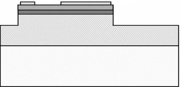
Fig. 2-1. Process flow and cross section of nitride-based LEDs. Fig. 2-2. The scheme of transmittance measurement method. Fig. 2-3. A transmission line model test structure.
Fig. 2-4. A plot of total resistance as a function of contact spacing, d. Fig. 2-5. A schematic diagram of a typical SEM.
Fig. 3-1. RS of (a) 300 nm, (b) 180 nm ITO films on quartz after different processes. Fig. 3-2. RS of different thicknesses of ITO films evaporated with (a) 15 sccm, (b) 30
sccm O2 flow rate.
Fig. 3-3. SEM pictures of ITO films with thickness of (a) 60 nm, (b) 180 nm, (c) 300 nm.
Fig. 3-4. Transmittance of 300 nm ITO on GaN substrate after annealed at different temperatures (O2 = 15sccm).
Fig. 3-5. Transmittance of different thicknesses of ITO films (O2 = 15 sccm). Fig. 3-6.I-V characteristics for Ni/Au (4 nm/4 nm) and ITO (300 nm) contacts on
p-GaN after annealing at temperatures of 400-600℃ (O2 = 15 sccm), measured between the TLM pads with a spacing of 20 μm.
Fig. 3-7. The fitting diagram of measured data. The ITO film is 300 nm thick and was evaporated with 15 sccm O2 flow rate.
Fig. 3-8. Specific contact resistances of ITO films on p-GaN which were evaporated with different oxygen flow rates and annealed at 400-600℃. The thickness of ITO is 300 nm.
Fig. 3-9. Calculated current distribution vs. the lateral length x in a LED. The O2 flow rate is (a) 15 sccm and (b) 30 sccm, and annealing temperatures are both 400 ℃.
Fig. 3-10. Calculated current spreading length of different thicknesses of ITO films. The oxygen flow rate during evaporation is 15 sccm.
Fig. 3-11. Calculated current spreading length of 300 nm ITO films which were evaporated with different oxygen flow rates.
Fig. 3-12. Reverse voltage-current characteristics of the fabricated nitride-based LEDs with different annealing temperatures. The thickness of ITO film is 300 nm and evaporated with 15 sccm O2 flow rate.
Fig. 3-13. The reverse I-V characteristics of devices on (a) condition B and (b) condition F.
Fig. 3-14. Forward current-voltage characteristics of GaN LEDs with different thicknesses of ITO films which were annealed at 400℃ and evaporated with (a) O2 = 15 sccm (b) O2 = 30 sccm.
Fig. 3-15. Forward current-voltage characteristics of GaN LEDs with 300 nm ITO films annealed at different temperatures and evaporated with (a) O2 = 15 sccm (b) O2 = 30 sccm.
Fig. 3-16. Forward voltage vs. dynamic resistance in LEDs with ITO film annealed at 400℃ and evaporated with (a) 15 sccm and (b) 30 sccm O2 flow rate. Fig. 3-17. The normal luminance vs. injection current of fabricated LEDs with 300
nm ITO film evaporated with (a) 15 sccm and (b) 30 sccm O2 flow rate. Fig. 3-18. The luminance enhancement vs. injection current of fabricated LEDs with
(a) 60 nm and (b) 300 nm ITO film evaporated with 15 sccm O2 flow rate. Fig. 3-19. Luminance enhancement with different ITO films at an injection current of
20-100 mA
Fig. 3-20. Normal luminance of all ITO samples at an injection current of (a) 20 mA, and (b) 50 mA. Conditions are referred to table 2-1.
Fig. 3-21. Emission microscopy graphs of (a) condition B annealed at 400℃ and (b) normal LED at a dc current of 0.2 mA.
Fig. 3-22. The relationship between current spreading length and (a) forward voltage at 20 mA and (b) normal luminance.
Fig. 3-23. The current converting efficiency (dL/dI) of LEDs vs. injection current. The ITO films were evaporated with 15 sccm O2 flow rate and annealed at 500 ℃.
Chapter 1
Introduction
1.1 An Overview of GaN-based Light-Emitting Diodes
Group III-nitride semiconductors have attracted much attention for versatile applications because of their unique properties such as wide direct band gap, high thermal conductivity, and chemical stability. GaN-based materials have also been of great interest and play an important role in solid-state lighting in the green, blue and violet light regions [1-5]. Since the brightness of GaN-based light emitting diodes is increased, the application of LEDs is widened such as displays, traffic signals, backlight for cell phones, exterior automotive lighting and so on. Especially, there is a lot of speculation about white LEDs for general illumination by using the high brightness LEDs.
1.2 Transparent Conducting Layer of LEDs
Although the brightness of LEDs continues increasing, the total light output is still quite low compared to that of a conventional light source [6]. Most commercial GaN-based LEDs use an Mg-doped GaN layer as a p-type semiconductor [7-9]. However, the high activation energy (~180 meV) of Mg atoms leads to a low ionization rate. There is only 1% of Mg atoms can be ionized, and therefore the carrier concentration of p-type GaN is quite low and the poor conductivity will limit current spreading laterally. It is necessary to deposit a conductive layer on p-GaN for current spreading. This layer should not only form good ohmic contacts to p-GaN but also be transparent to the emitted light from the active layer. Considering the high work function of p-GaN, metals of high work functions such as Ni, Pd, and Pt were used to form p-type ohmic contacts [10-14]. The specific contact resistance around 10-2 ~ 10-6
Ω·cm2 were obtained when the samples were annealed at temperatures of 400 ~ 600℃ in air. Thin Ni/Au films were deposited on Mg-doped GaN to act as transparent conductive layers in the conventional GaN-based LEDs structures. The mechanism of ohmic contacts formation is studied by Ho et al. The main concept is to use p-type NiO with nickel vacancies and/or oxygen interstitials contacts to p-GaN to reduce interface resistance. The high carrier concentration of NiO makes a metal easy to achieve an ohmic on it. However, the Au-based contacts generally have poor thermal stability, leading to poor device reliability. And it has also been reported that the transmittance of Ni/Au is only around 60% to 85% in the 450-550 nm wavelength [15]. The transmittance of conducting layer is important for the LEDs since photons generated in the active region will be partially absorbed by this layer. Although the thickness of Ni/Au can be reduced to increase the transmittance, the contact reliability could be a serious issue when the thickness becomes too small. If we could increase the conducting layer transmittance, we should be able to increase the LED output intensity. In other words, to achieve high performance GaN-based LEDs, it is required to reduce p-contact resistance and to enhance transmission efficiency of p-contact metal layer simultaneously. To reduce p-contact resistance, we have recently demonstrated GaN-based LEDs incorporated with and n+-InGaN-GaN short-period-superlattice (SPS) tunneling contact layer which have low operating voltages [16, 17]. By growing such SPS structure on top of the p-GaN cap layer, one could achieve a good ohmic contact via tunneling when the n+(InGaN/GaN)-p(GaN) junction was properly reverse biased. And to improve the transmittance of current spreading layer, it is feasible to replace the conventional Ni/Au contact by a better transparent conductive contact. Nowadays, transparent conductive oxide materials (TCO), such as aluminum-doped zinc-oxide (AZO) [18], gallium-doped zinc-oxide [19], cadmium-tin-oxide (CTO) [20], and indium-tin-oxide (ITO) [21], are applied to
optical electrical devices. Moreover, the ITO film has been widely used as a transparent conductor due to its high transparency (~90%) in the visible spectrum and its low electrical resistivity (< 5×10⁻⁴ Ω·cm). The ITO film can also provide high carrier concentration (1020-1021 cm-3) and applicable mobility (25-50 cm2/V·s). All of these advantages render ITO an attractive material for fabricating GaN-based LEDs. However, a good ohmic contact can only be achieved when ITO is deposited on n-GaN, while a Schottky contact is formed when ITO is deposited instead on p-GaN. As a result, the operating voltages for GaN-based LEDs with ITO p-contacts were still too large for practical device applications. The other possible way is to use Ni/ITO. Previously, Horng et al. have reported that Ni/ITO could form good ohmic contact on p-GaN [22]. The Ni metal was utilized as an intermediate layer between ITO and p-GaN for the study of optimum ohmic contact. The ITO film not only provides the oxide source for NiO formation, but also preserves high conductivity and high transparency. By using Ni/ITO instead of ITO as the transparent conducting layer (TCL) in GaN-based LEDs, the lower forward voltage and higher reliability can be achieved [23-26]. This intermediate metal can be replaced by other materials. Song et
al. have reported that using Ag/ITO as TCL exhibits greatly improved electrical
characteristics, yielding specific contact resistance of ~10-4 Ω·cm2 [27].
1.3 Motivation
ITO has been widely used as TCL in the fabrication of GaN-based LEDs. However, the optimal thickness for high performance device is still not clearly known. In this study, we adopt different thicknesses of ITO films as TCLs and investigate the influence on optical and electrical characteristics of devices. In addition, the oxygen flow rate during ITO evaporations and post annealing temperature are also discussed. The thickness is set to be a quarter light wavelength as following,
m n t ITO ITO × × = 4 λ (m = 1, 3, 5…..) (Eq. 1-1) where λ, tITO, and nITO is the wavelength of the incident light, the thickness and refractive index of ITO, respectively. The calculated thickness is about 60 nm, 180 nm, and 300 nm when the factor m is chosen to be 1, 3, and 5, respectively. These thicknesses are designed to avoid additional light deprivation.
In our experiment, we used Cr-Au as the bonding pad. Chromium was employed for current blocking layer (CBL). In conventional designs, light generated under the opaque p-pad metal electrode is absorbed or reflected by the contact and lost. However, the Cr/p-GaN interface forms a schottky contact. In the CBL design, the area under the p-pad metal electrode is selectively given a relative high resistance, reducing current flow and light generation under the contact. Thus, the current normally passing through the CBL region is instead distributed over the useful area of the device. The similar ideas also appeared in other papers [28, 29].
1.4 Thesis Organization
In chapter 1, a brief overview of LEDs and related developments were introduced.
In chapter 2, the fabrication process flow of LEDs, experimental recipes, and device parameter extraction methods will be described.
In chapter 3, we will show and discuss the characteristics of ITO film, ITO/p-GaN interface, and LED device, including sheet resistance, transmittance, specific contact resistance, I-V and L-I characterization.
In chapter 4, a short conclusion is addressed.
Finally, future works as well as suggestion for further research are given in chapter 5
Chapter 2
Experiment
2.1 The Process Flow of LEDs
The GaN-based LED epi-wafers used in this study were all grown on a 2-inch-diameter c-face sapphire (0001) substrates by metal-organic chemical vapor deposition (MOCVD) system. Details of the growth procedures could be found elsewhere [30, 31]. The epitaxial structure is consisted of 4-μm-thick n-type GaN layer, 0.1-μm-thick InGaN-GaN multiple-quantum-wells (MQWs), and 0.1-μm-thick p-type GaN layer. The carrier concentrations of the p-type and n-type GaN were 5×10¹⁷ and 3×1018 cm-3, respectively. The as-grown samples were rapidly thermal annealed (RTA) at 800 for Mg℃ -type activation. All wafers with a peak wavelength at 465 nm were chosen and cut into four pieces for different processes. One piece of each wafer was prepared for the conventional LEDs with Ni/Au (4nm/4nm) contact structure as a reference sample. The other pieces were prepared as experimental samples with ITO contacts of different thicknesses and annealed at different temperatures.
GaN-based LEDs (300 × 300 μm) with different conducting layers were fabricated.Figure 2-1 shows the cross section and process flow of LEDs. By means of photoresist lithography, the mesa region could be defined after removing photoresist. The surface of p-type GaN layer was partially etched by an inductance-coupled plasma (ICP) etcher until the n-type GaN layer was exposed. Then these samples were immersed in H2SO4 : H2O2 and NH4OH : H2O solutions to remove photoresist mask and residue chemical oxides. Next, ITO was deposited on samples by E-beam evaporator at 300 in oxygen ambience.℃ The ITO source consisted of 95% In2O3 and 5% SnO2. The thicknesses of ITO were 60 nm, 180 nm and 300 nm with different
oxygen flow rates, as listed in table 2-1. The base pressure was 5×10⁻⁶ torr and working pressure was 2.2×10⁻⁴ torr and 4.5×10⁻⁴ torr when oxygen flow rate was 15 sccm and 30 sccm, respectively. ITO was also deposited on double-side-polished GaN wafers and quartz substrates for transmission studies. The Ni/Au (4nm/4nm) contact layer was deposited by E-beam evaporator with a base pressure of 2×10⁻⁶ torr. After lithography process, these ITO and Ni/Au contact samples were wet etched by ITO etchant and KI : HCl solution, respectively. Then, all samples with different thicknesses of ITO films were subsequently annealed in nitrogen ambience for 10 minutes at 400 , 500 , and 600 , respectively. As for the ℃ ℃ ℃ Ni/Au contact sample, it was annealed at 540 in nitrogen ambience to achieve the optimal ohmic contact to ℃ p-GaN. Finally, Cr-Au (0.1 μm/1.4 μm) was used as the n-type contact layer, p- and n-bonding pads. Cr was used for the CBL, as mentioned above.
After fabrication processes, the sheet resistance was measured using a four-point probe. In order to truly exhibit the effects of absorption, internal reflection and interference of the conducting films on GaN-based LEDs, the p-i-n GaN with a double-side-polished sapphire substrate was used in the transmittance measurement. The transmission spectra of the deposited films were measured by a Hitachi U3010 dual-beam spectrophotometer. Scanning electron microscope (SEM) was used to observe the grain size of ITO with different thicknesses.
Test keys consisting of transmission line model (TLM) patterns were used for calculating the specific contact resistance of the conducting layers on p-GaN and sheet resistance of p-GaN. After the sheet resistance and specific contact resistance of all samples were known, we created a calculation for checking the behavior of current distribution and calculating the current spreading length.
The current-voltage (I-V) characteristics were measured at room temperature using a HP4156A semiconductor parameter analyzer with a voltage source. The
relationship between LED output power and injection current (L-I) was also be measured by the integrated sphere detector from top of the devices.
The detailed fabrication process flow is listed as follows: 1. As-grown GaN wafer on (0001) sapphire substrate. 2. Initial cleaning (H2SO4 : H2O2).
3. Mask #1: Define mesa region. 4. Dry etching by ICP-RIE.
5. Photoresist removing and cleaning (H2SO4 : H2O2, NH4OH : H2O). 6. TCL evaporation (ITO with 60~300 nm and Ni/Au with 4/4 nm). 7. Mask #2: Define TCL region.
8. Etching TCL and removing photoresist.
9. TCL alloy for 10 minutes in furnace (400~600 for ITO and ℃ 540 for ℃ Ni/Au). 10. Mast #3: Define pad region.
11. P/N bonding pad metal evaporation (Cr-Au with 0.1/1.4 μm). 12. Removing metal by lift-off procedure.
13. P/N bonding pad alloy at 510 for 5 minutes in furnace℃ for Ni/Au samples.
2.2 Methods of Measurements and Analysis
2.2.1 The Transmittance of ITO Film
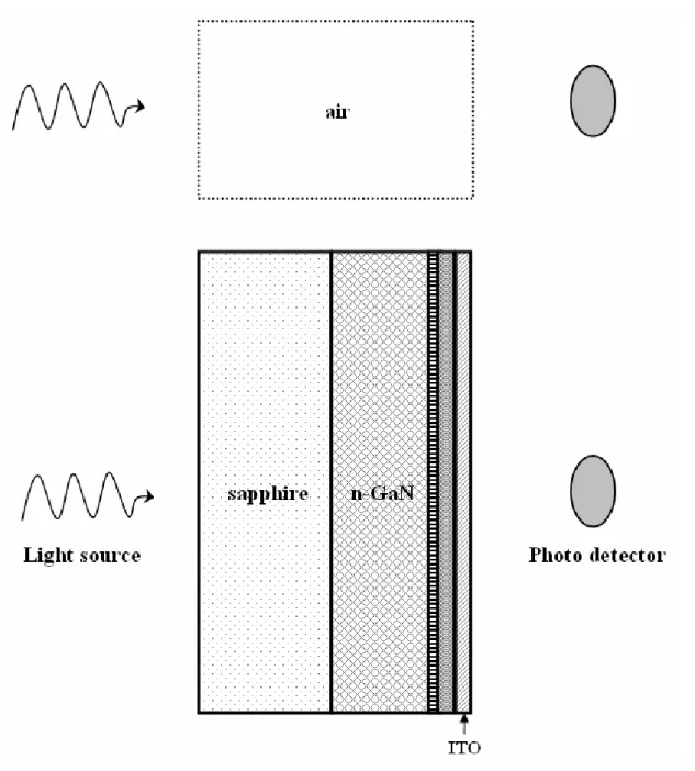
Before every optical transmittance measurement by the Hitachi U3010 spectrophotometer, the wavelength calibration had been done to ensure the credibility of measured data. The transmittance of each film was normalized with respect to air, as shown in Fig. 2-2. The light passed through ITO film to the air, as same as the actual situation.
2.2.2 Transmission Line Model (TLM)
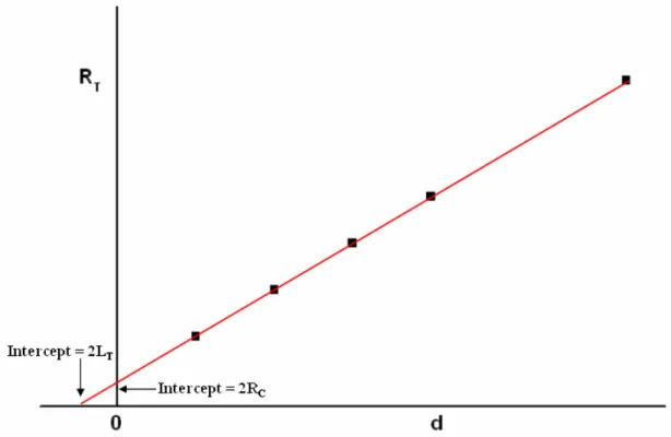
The transmission line model (TLM) was used for calculating the specific contact resistance of the conducting layers on p-GaN and sheet resistance of p-GaN. The pad size was 280×75 μm and the spacings between the pads were 10, 20, 30, 40, and 65 μm. A simple diagram of TLM pattern is shown in Fig. 2-3. We found the total resistance between any two contacts to be
(
T S C S T d L Z R R Z d R R = +2 ≈ +2)
(Eq. 2-1)where RT and RS is the total resistance and contact resistance of p-GaN, and we had used the approximation (The transfer length
S c T
R r
L = , rc is the specific contact resistance). The total resistance was measured for various contact spacings d and RT was plotted as function of d as illustrated in Fig. 2-4. Three parameters could be extracted from such a plot. The slope Δ(RT)/ Δ(d) = RS/Z led to the sheet resistance with the contact width Z independently measured. The intercept at d = 0 was RT = 2RC giving the contact resistance. The intercept at RT = 0 gives –d = 2LT, which in turn could be used to calculate the specific contact resistance with RS known from the slope of the plot.
2.2.3 Calculation of Current Spreading Length
After obtaining the sheet resistance of ITO film and the contact resistivityof ITO/p-GaN, we calculated the current distribution and defined current spreading length by creating an equivalent LED circuit [32-35]. The current distribution can be denoted by this equation
( )
( )
(
)
⎟⎟⎟ ⎟ ⎟ ⎟ ⎠ ⎞ ⎜ ⎜ ⎜ ⎜ ⎜ ⎜ ⎝ ⎛ − + − = −1 exp 0 t t n n p p c t t t x J x J ρ ρ ρ ρ (Eq. 2-2)where J(0) is the current density at p-pad site and the parameters ρp, ρn, ρt, tp, tn, and tt are the electrical resistivities and thicknesses of p, n, and transparent layer. Variable x represents the distance from p-pad. Denoting Ls, current spreading length, as the length where the current density has dropped to the 1/e value of the current density at the p-pad, i.e., J(Ls)/J(0) = 1/e, yields
(
+)
− −1 = t t n n p p c s t t t L ρ ρ ρ ρ (Eq. 2-3)We will check if the current spreading length corresponds to device luminance later.
2.2.4 Current-Voltage Characteristic Measurement
The current-voltage (I-V) characteristics were measured at room temperature using a HP4156A semiconductor parameter analyzer with a voltage source. Ten devices of each sample were measured in order to choose a most reliable one to serve as the result. The relationship between LED output power and injection current (L-I) was also be measured by the integrated sphere detector from top of the devices. Each ITO sample was compared and normalized with Ni/Au sample which were cut from the same wafer to ensure a reliable result.
2.2.5 The Introduction of Scanning Electron Microscope (SEM)
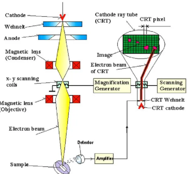
Electron microscopy takes advantage of the wave nature of rapidly moving electrons. Where visible light has wavelengths from 4,000 to 7,000 Angstroms, electrons accelerated to 10,000 KeV have a wavelength of 0.12 Angstroms. Optical
microscopes have their resolution limited by the diffraction of light to about 1000 diameters magnification. Electron microscopes, so far, are limited to magnifications of around 1,000,000 diameters, primarily because of spherical and chromatic aberrations. Scanning electron microscope resolutions are currently limited to around 25 Angstroms, though, for a variety of reasons. A schematic diagram of a typical SEM is shown in Fig.2-5.
The scanning electron microscope generates a beam of electrons in a vacuum. That beam is collimated by electromagnetic condensor lenses, focussed by an objective lens, and scanned across the surface of the sample by electromagnetic deflection coils. The primary imaging method is by collecting secondary electrons that are released by the sample. The secondary electrons are detected by a scintillation material that produces flashes of light from the electrons. The light flashes are then detected and amplified by a photomultiplier tube.
By correlating the sample scan position with the resulting signal, an image can be formed that is strikingly similar to what would be seen through an optical microscope. The illumination and shadowing show a quite natural looking surface topography.
There are other imaging modes available in the SEM. Specimen current imaging using the intensity of the electrical current induced in the specimen by the illuminating electron beam to produce an image. It can often be used to show subsurface defects. Backscatter imaging uses high energy electrons that emerge nearly 180 degrees from the illuminating beam direction. The backscatter electron yield is a function of the average atomic number of each point on the sample, and thus can give compositional information.
Scanning electron microscopes are often coupled with x-ray analysers. The energetic electron beam - sample interactions generate x-rays that are characteristic of
the elements present in the sample. Many other imaging modes are available that provide specialized information.
2.2.6 The Introduction of HP4156A
HP4156A is an electronic instrument for measuring and analyzing the characteristics of semiconductor devices. This one instrument allows us to perform both measurement and analysis of measurement results.
HP4156A has four highly accurate source/monitor units (SMUs), two voltage source units (VSUs), and two voltage measurement units (VMUs). The HP4156A is designed for Kelvin connections and has high-resolution SMUs (HRSMUs), so HP4156A is especially suited for low resistance and low current measurements. We can measure voltage values with a resolution of 0.2μV by using the differential measurement mode of VMUs.
HP4156A can perform stress testing. That is, can force a specified dc voltage or current for the specified duration.
Also, we can force ac stress by using pulse generator units (PGUs), which are installed in HP41501A SMU/Pulse Generator Expander. The HP41501A is attached to HP4156A, and can be equipped with a ground unit (GNDU), high power SMU (HPSMU), two medium power SMUs (MPSMUs), or two PGUs.
HP4156A can print and store, in addition to performing measurement and analysis. We can store measurement setup information, measurement data, and instrument setting information on a 3.5-inch diskette inserted into the disk drive of HP4156A. And we can print the setting information and measurement results on a plotter or printer that is connected to HP4156A.
HP4156A can be controlled by an external controller via HP-IB by using remote control commands. These commands are based on Standard Commands for
Programmable Instruments (SCPI), so we can easily develop measurement programs. HP4156A has internal HP instrument BASIC, so we can develop and execute measurement programs by using the HP4156A only, without using an external controller.
Chapter 3
Results and Discussion
3.1 Properties of Films
3.1.1 Sheet Resistance of ITO Film
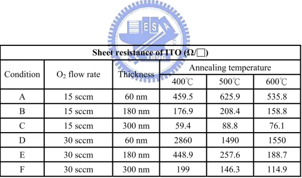
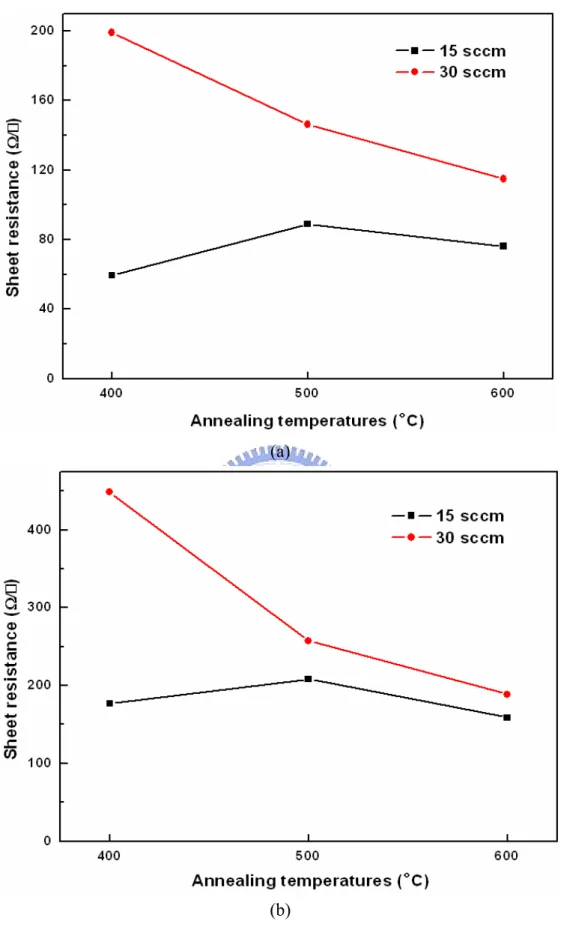
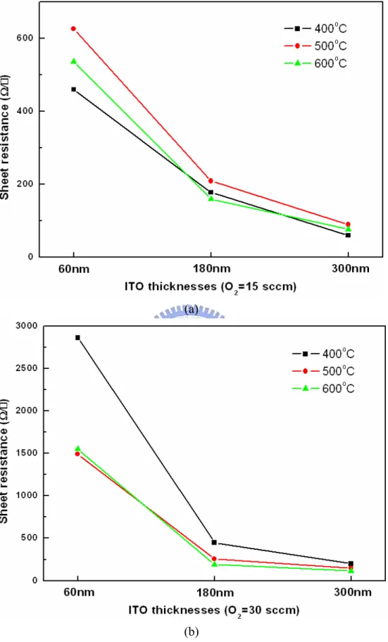
Figure 3-1 shows the sheet resistance of 180 nm and 300 nm thick ITO films which were evaporated on quartz substrates at two oxygen flow rates. When the flow rate is 30 sccm, we can find the sheet resistance decreasing after annealing at higher temperature. On the other hand, if the oxygen flow rate is 15 sccm, sheet resistance will have a maximum value after 500 annealing℃ . The appearances are similar on different thicknesses of ITO films. It is well known that the oxygen content in ITO films is a critical control parameter of the resistivity of the film. Conduction is partially a result of unfilled oxygen vacancies, so a high incorporation of oxygen into the film will result in few vacancies and a highly resistive film [36]. When annealing at higher temperature, the oxygen atoms may easily evaporate to the air. It will increase the amount of oxygen vacancies and attribute to a better conductivity of ITO film. Figure 3-2 shows the relationship between ITO film thickness and the sheet resistance. By any means, the sheet resistance decreases while increasing the thickness of ITO film due to a higher conductivity, as our preconception. The measured sheet resistances of all ITO films are listed in table 3-1.
3.1.2 Scanning Electron Microscope (SEM) Analysis
Figure 3-3 shows SEM pictures of ITO films with different thicknesses. ITO films were observed to be polycrystalline and showed a similar crystal structure to that of undoped In2O3. The grain size is about 70 nm, 120 nm, and 160 nm for 60 nm, 180 nm, and 300 nm ITO film, respectively. These pictures indicate that the grain size
of the films increased with growing film thickness. In the thin film growth, it is generally observed that the grain size increases with increasing film thickness [37, 38]. The larger grain size results in a lower density of grain boundaries, which behave as traps for free carriers and barriers for carrier transport in the film [39]. Hence, an increase in the grain size can cause a decrease in grain boundary scattering, which leads to an increase in the conductivity. It may be one reason of why thicker ITO film got a smaller sheet resistance.
3.1.3 Transmittance of ITO Film
Figure 3-4 shows the optical transmittance as a function of wavelength of the evaporated ITO film on GaN substrate with different annealing temperatures. In this figure, the transmittance of each film was directly compared with air. By varying the annealing temperature, the transmittances are almost the same. However, the curves were long-wavelength shifted after annealed at higher temperature. It means an increase of the refractive factor of ITO film. The transmittance of different ITO film thicknesses are showed in Fig. 3-5. For comparison, the most commonly used Ni(4 nm)-Au(4 nm) contact layer that was annealed at 540℃ in nitrogen ambience was also examined. The transmittances are about 80% at a wavelength of 465 nm of all thicknesses of ITO films. Compared with Ni/Au film, transmittance of ITO has an enhancement of about 20%.
3.2 Interfacial Characteristics
3.2.1 Specific Contact Resistance of ITO or Ni/Au Layer on p-GaN
Figure 3-6 shows the current-voltage (I-V) characteristics of Ni/Au (4 nm/4 nm) and ITO (300 nm) contacts on p-GaN after annealing at temperatures of 400-600 ℃ for 10 minutes in N2 ambient. It was found that both ITO and Ni/Au films could form
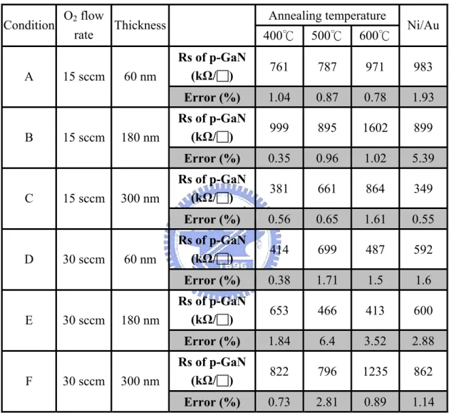
good ohmic contacts on p-GaN. Specific contact resistance was determined from plots of the measured total resistance versus the spacings between the TLM pads. The least square curve-fitting method was used to fit a straight line to the experimental data, as shown in Fig. 3-7. Although ITO and Ni/Au films both have ohmic contacts on p-GaN, Ni/Au still has the smaller specific contact resistance than all ITO films. To explain the low resistance of Ni/Au contacts, Ho et al. proposed that NiOx layer on the p-GaN epilayer surface causes a reduction of the schottky barrier height across the interface [40]. However, Maeda et al. suggested that oxygen reacts with hydrogen in the Mg-H bonds and, thus, reduces the hydrogen concentration and modifies the energy band structure in the interface region [41]. Moreover, another study suggested that ohmic contact characteristics result from the removal of surface contamination on GaN by Ni before or during layer reversal [42]. Figure 3-8 exhibits the specific contact resistances of ITO films on p-GaN which were evaporated with different oxygen flow rates and annealed at 400-600 .℃ It is obvious that the specific contact resistance had a minimum value at 500℃ with 15 sccm O2 flow rate and increased with the annealing temperature with 30 sccm O2 flow rate. This may be due to the variance of oxygen proportion in the ITO/p-GaN interface which will combine with gallium to form GaO. Moreover, ITO films that were evaporated with 30 sccm oxygen flow rate have a higher specific contact resistance than with 15 sccm. This may be due to the incorporation of oxygen. The relationship between specific contact resistance and ITO film thickness is not discussed because the thickness should not affect the interface characteristics. A particular data of all samples’ specific contact resistance is listed in table 3-2. The sheet resistance of p-GaN was also calculated simultaneously and is listed in table 3-3. The fluid values of p-GaN’s sheet resistance may be attributed to the instability of carrier concentration. However, the sheet resistance of p-GaN is larger than that of ITO film and result in a poor conductivity. That’s why we need an
additional transparent conducting layer upon p-GaN.
3.2.2 Current Spreading Behavior by Calculation
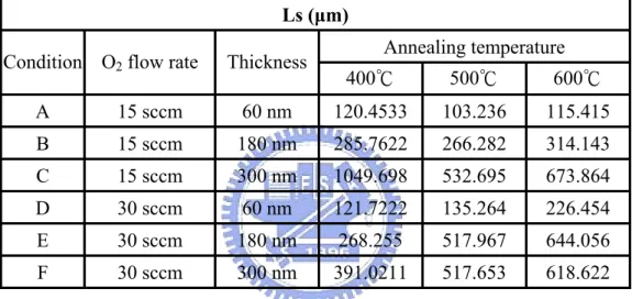
After the sheet resistances and specific contact resistances were known, we started the current spreading calculation. The calculated current distribution of the LED is shown in Fig. 3-9. As the results by calculation, we can conclude that thicker ITO film contributes to a uniform current spreading phenomenon. This instance is chiefly caused by the smaller sheet resistance of thicker film. It can be seen that current crowding can be alleviated via the use of a thicker ITO film. For simple expression, we define current spreading length Ls as the length where the current density has dropped to the 1/e value of the current density at the p-pad. Figure 3-10 shows the calculated current spreading length of different thicknesses of ITO films that were evaporated with 15 sccm oxygen flow rate. This figure indicates that no matter at what annealing temperature, current will spread farther by increasing ITO film’s thickness due to the lower sheet resistance. Figure 3-11 shows Ls of 300 nm ITO films which were evaporated with different oxygen flow rates. With a 30 sccm oxygen flow rate during evaporation, sample annealed at 600℃ has a longest Ls compared with other temperatures because of its largest specific contact resistance. The large specific contact resistance makes the current tend to flow horizontally. Same theory can also explain the shortest Ls at 500 with 15 s℃ ccm oxygen flow rate by having the smallest specific contact resistance. Ls of ITO samples are listed together in table 3-4.
3.3 Electrical and Optical Properties of Devices
3.3.1 Reverse Current-Voltage Characteristic of LEDsvalue of leakage current, as shown in Fig. 3-12. The leakage current is only several nA which is small enough as our toleration, and not affected by annealing temperature. The fabricated LEDs’ leakage currents are generally small enough except two wafers. Figure 3-13 points out the high leakage current of these devices with 180 nm ITO film evaporated with 15 sccm oxygen flow rate and annealed at 400℃. It may be caused by the bad epitaxy property of GaN wafer and will result in the output power’s degradation and a serious thermal effect.
3.3.2 Forward Current-Voltage Characteristic of LEDs
Figure 3-14 depicts the room-temperature forward current-voltage characteristics of the fabricated GaN-based LEDs. These samples were all annealed at 400 .℃ In Fig. 3-14(a), the 20-mA forward voltage measured from LEDs with 60 nm ITO, 180 nm ITO, 300 nm ITO, and Ni/Au on p-GaN was 3.45, 3.41, 3.32, and 3.14 V, respectively. Apropos of LEDs with films which were evaporated with high oxygen flow rate, the forward voltage was 3.5, 3.31, 3.26, and 3.08 V, respectively, as shown in Fig. 3-14(b). The forward voltage decreases with an increase of ITO film’s thickness. As the specific contact resistance doesn’t form an order, the forward voltage may be affected by sheet resistance, or conductivity of TCL. We can read from the figure that Ni/Au film still has the smallest Vf due to its corking conductivity. Figure 3-15 shows the comparison of forward voltage with different annealing temperature. In Fig. 3-15(a), the 400℃-annealed sample’s large forward voltage is attributed to the large specific contact resistance. Similarly, in Fig. 3-15(b), the forward voltage is also affected by the specific contact resistance.
3.3.3 Dynamic Resistance and Series Resistance of LEDs
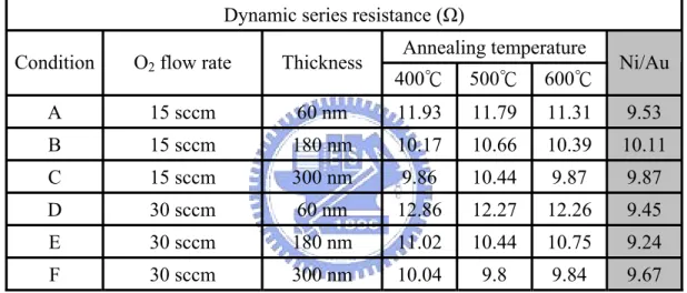
with different thicknesses of ITO films annealed at 400 .℃ The dynamic resistance decreases while the voltage increases because more and more free electron-hole pairs are generated. Values at the tail of the curves are close to their own series resistance. It can be seen that the series resistance is in association with the thickness of ITO film. The approximated series resistances are listed in table 3-5. All series resistances have a decrease with thicker ITO films. While the ITO’s thickness is fixed, annealing temperature almost has no influence on the series resistance. Thus, we can conclude that the series resistance is mainly dominated by sheet resistance. Hence, Ni/Au film’s small series resistance is reasonable due to its good current spreading ability.
3.3.4 Luminance-Current Characteristic of LEDs
Figure 3-17 presents the normal light output as a function of injection current for fabricated LEDs with 300 nm ITO film annealed at different temperatures. Devices with ITO film are all brighter than that with Ni/Au film. Figure 3-18 shows the luminance enhancement as a function of injection current for LEDs with different thicknesses of ITO films. The ITO samples were compared and normalized with Ni/Au samples which were cut from the same wafer to ensure a reliable result. We could achieve a factor of about 1.3-1.5 times luminance enhancement by the difference of optical transmittance between ITO and Ni/Au films. Notice that the enhancement of devices with 60 nm ITO film has a decrease when the injection current increasing. On the other hand, devices with 300 nm ITO film don’t have such a decrease. It is supposed that because the thin ITO film has a heavier thermal effect than thick ITO film and Ni/Au film. The heavy thermal effect is attributed to the poor conductivity which forms a large resistance. Figure 3-19 presents the luminance enhancement with different ITO films at an injection current of 20-100 mA. No matter what the evaporating oxygen flow rate is, the thermal effect is serious with thin
(60 nm) ITO films while thick (300 nm) ITO films almost remain the enhancement factor in constant. Normal luminance of all ITO samples at different injection current is shown in Fig. 3-20. From Fig. 3-13, we have known that the leakage current in condition B is extremely high, especially in the 400 annealing one.℃ It will cause the degradation of output light, as shown in Fig. 3-21. The high density of black dots in Fig. 3-21(a) is caused by the high leakage current. Hence, the circled data in Fig. 3-20 may not be accurate. In addition, it seems that the luminance of each device doesn’t form a regular relationship. Figure 3-22 shows the relationship between calculated current spreading length and forward voltage or normal luminance. From Fig. 3-22(a), we find that LS decreases while the forward voltage increasing, where the straight line is an approximation line fitted by least square method. This may be resulted by the specific contact resistance. A large rC will cause a long current spreading length and a small 20-mA forward voltage. However, in Fig. 3-22(b), it seems that the optical performance is not corresponding to current spreading length. A possible reason is that most of the current spreading lengths are larger than the device size (300 × 300 μm), so almost all devices have a uniform enough current distribution. Figure 3-23 shows the current converting efficiency (dL/dI) of LEDs as a function of injection current. When the injection current becomes larger, a decrease of the converting efficiency could be discovered. It may be a reason of why the luminance has no relationship with LS. Although thicker ITO film has longer current spreading length, the increment in light output is not as much as in the current density. Then, such declined light enhancement may be disrupted because the thickness of evaporated ITO film might not be exact enough as our settings.
Chapter 4
Conclusion
In this experiment, we have fabricated GaN-based LEDs with different thicknesses of ITO films and also found the optical and electrical characteristics of them. First, we observe that the sheet resistance of ITO films on quartz has a decrease when the films grow thicker, which indicates a better conductivity. However, the sheet resistance is also dominated by the annealing temperature due to the change of the amount of oxygen vacancies and grain size of ITO film. From SEM pictures, we can discover that the grain size of ITO film has an obvious increase with its thickness. Next, the transmittances of these ITO films are all about 80% at a wavelength of 465 nm and have 20% larger than Ni/Au films.
Moreover, the specific contact resistance increases with the annealing temperature, which is attributed to a thin GaO layer formed in the ITO/p-GaN interface. The calculated current distribution and current spreading length are affected by sheet resistance and specific contact resistance, especially the sheet resistance. A small sheet resistance, or a thick ITO film, demonstrates a good current spreading ability. Some of the calculated current spreading lengths are even larger than the size of LED device. The thickness of ITO film is also corresponding to the operating voltage due to the variance of conductivity. However, the film thickness seems no relationship with the normal light output. Compared with the references, all LEDs with different ITO films have a factor of about 1.3-1.5 times luminance enhancement by the difference of optical transmittance. By generalizing the above results, the best thickness of ITO film can be 300 nm.
Chapter 5
Future Work
In the future work, the similar experiment for other TCL structures with an intermediate metal layer, such as Ni/ITO and Ag/ITO, will be carried out. Larger size LEDs can even be fabricated because the current spreading length of a thick ITO film can be in excess of 1000 μm. In addition, after finding the best thickness of ITO film, it will be combined with surface roughening technique to achieve higher light extraction efficiency. This may help fabricating LEDs with an additional luminance enhancement.
Reference
[1] S. Nakamura, T. Mukai, and M. Senoh, “Candela-class high-brightness InGaN/AlGaN double-heterostructure blue-light-emitting diodes,” Appl. Phys.
Lett., vol. 64, pp. 1687-1689, 1994.
[2] S.Nakamuram M. Senoh, N. Iwasa, and S. Nagahama, “High-power InGaN single-quantum-well-structure blue and violet light-emitting diodes,” Appl. Phys.
Lett., vol. 67, pp. 1868-1870, 1995.
[3] T. Mukai and S. Nakamura, “Ultraviolet InGaN and GaN single-quantum-well-structure light-emitting diodes grown on epitaxially laterally overgrown GaN substrates,” Jpn. J. Appl. Phys., vol. 38, pp. 5735-5739, 1999. [4] S. Nakamura, M. Senoh, S. Nagahama, N. Iwasa, T. Yamada, T. Matsushita, Y.
Sugimoto, and H. Kiyoku, “Room-temperature continuous-wave operation of InGaN multi-quantum-well-structure laser diodes with a long lifetime,” Appl.
Phys. Lett., vol. 70, pp. 868-870, 1997.
[5] S. Nakamura, M. Senoh, S. Nagahama, N. Iwasa, T. Yamada, T. Matsushita, H. Kiyoku, Y. Sugimoto, T. Kozaki, H. Umemoto, M. Sano, and K. Chocho, “Continuous-wave operation of InGaN/GaN/AlGaN-based laser diodes grown on GaN substrates,” Appl. Phys. Lett., vol. 72, pp. 2014-2016, 1998.
[6] J. J. Wierer, D. A. Steigerwald, M. R. Krames, J. J. O’Shea, M. J. Ludowise, G. Christenson, Y. -C. Shen, C. Lowery, P. S. Martin, S. Subramanya, W. Gotz, N. F. Gardner, R. S. Kern, and S. A. Stockman, “High-power AlGaInN flip-chip light-emitting diodes,” Appl. Phys. Lett., vol. 78, pp. 3379-3381, 2001.
[7] C. H. Chen, S. J. Chang, Y. K. Su, J. K. Sheu, J. F. Chen, C. H. Kuo, and Y. C. Lin, “Nitride-based cascade near white light-emitting diodes,” IEEE Photon. Technol.
[8] C. H. Kuo, S. J. Chang, Y. K. Su, J. F. Chen, L. W. Wu, J. K. Sheu, C. H. Chen, a nd G. C. Chi, “InGaN/GaN light emitting diodes activated in O ambient,2 ” IEEE
Electron. Dev. Lett., vol. 23, pp. 240-242, 2003.
[9] C. H. Kuo, S. J. Chang, Y. K. Su, L. W. Wu, J. K. Sheu, C. H. Chen and G. C. Chi, “Low temperature activation of Mg-doped GaN in O2 ambient,” Jpn. J. Appl.
Phys., vol. 41, pp. L112-L114, 2002.
[10] J. K. Ho, C. S. Jong, C. C. Chiu, C. N. Huang, C. Y. Chen, and K. K. Shih, “Low-resistance ohmic contacts to p-type GaN,” Appl. Phys. Lett., vol. 74, pp. 1275-1277, 1999.
[11] L. Zhou, W. Lanford, A. T. Ping, I. Adesida, J. W. Yang, and A. Khan, “Low resistance Ti/Pt/Au ohmic contacts to p-type GaN,” Appl. Phys. Lett., vol. 76, pp. 3451-3453, 2000.
[12] J. K. Kim, J. L. Lee, J. W. Lee, H. E. Shin, Y. J. Park, and T. Kim, “Low resistance Pd/Au ohmic contacts to p-type GaN using surface treatment,” Appl.
Phys. Lett., vol. 73, pp. 2953-2955, 1998.
[13] J. S. Jang, S. J. Park, and T. Y. Seong, “Interfacial reaction of Ni/Pt/Au contact schemes to p-Type GaN,” J. Electrochem. Soc., vol. 146, pp. 3425-3428, 1999. [14] D. J. King, L. Zhang, J. C. Ramer, S. D. Hersee, and L. F. Lester, “Temperature
behavior of Pt/Au ohmic contacts to p-GaN,” Mater. Res. Soc. Symp. Proc., vol. 468, pp. 421, 1997.
[15] J. K. Sheu, Y. K. Su, G. C. Chi, P. L. Koh, M. J. Jou, C. M. Chang, C. C. Liu, and W. C. Hung, “High-transparency Ni/Au ohmic contact to p-type GaN,” Appl.
[16] J. K. Sheu, J. M. Tsai, S. C. Shei, W. C. Lai, T. C. Wen, C. H. Kou, and Y. K. Su, S. J. Chang, and G. C. Chi, “Low-operation voltage of InGaN/GaN light-emitting diodes with Si-doped In0.3Ga0.7N/GaN short-period superlattice tunneling contact layer,” IEEE Electron. Dev. Lett., vol. 22, pp. 460-462. 2001.
[17] S. J. Chang, C. S. Chang, Y. K. Su, R. W. Chuang, W. C. Lai, C. H. Kuo, Y. P. Hsu, Y. C. Lin, S. C. Shei, H. M. Lo, J. C. Ke, and J. K. Sheu, “Nitride-based LEDs with an SPS tunneling contact layer and an ITO transparent contact,”
IEEE Photon. Technol. Lett., vol. 16, pp. 1002-1004, 2004.
[18] J. O Song, K. K. Kim, S. J. Park, and T. Y. Seong, “Highly low resistance and transparent Ni/ZnO ohmic contacts to p-type GaN,” Appl. Phys. Lett., vol. 83, pp. 479-481, 2003.
[19] K. Nakahara, K. Tamura, M. Sakai, D. Nakagawa, N. Ito, M. Sonobe, H. Takasu, H. Tampo, P. Fons, K. Matsubara, K. Iwata, A. Yamada, and S. Niki, “Improved external efficiency InGaN-based light-emitting diodes with transparent conductive Ga-doped ZnO as p-electrodes,” Jpn. J. Appl. Phys., vol. 43, pp. L180-L182, 2004.
[20] D. R. Kammler, T. O. Mason, D. L. Young, and T. J. Coutts, “Thin films of the spinel Cd1 + xIn2–2xSnxO4 transparent conducting oxide solution,” J. Appl. Phys., vol. 90, pp. 3263-3268, 2001.
[21] T. Margalith, O. Buchinsky, D. A. Cohen, A. C. Abare, M. Hansen, S. P. DenBaars, and L. A. Coldren, “Indium tin oxide contacts to gallium nitride optoelectronic devices,” Appl. Phys. Lett., vol. 74, pp. 3930-3932, 1999.
[22] R. H. Horng, D. S. Wuu, Y. C. Lien, and W. H. Lan, “Low-resistance and high-transparency Ni/indium tin oxide ohmic contacts to p-type GaN,” Appl.
[23] Y. C. Lin, S. J. Chang, Y. K. Su, T. Y. Tsai, C. S. Chang, S. C. Shei, S. J. Hsu, C. H. Liu, U. H. Liaw, S. C. Chen, and B. R. Huang, “Nitride-based light-emitting diodes with Ni/ITO p-type ohmic contacts,” IEEE Photon. Technol. Lett., vol. 14, pp. 1668-1670, 2002.
[24] Y. C. Lin, S. J. Chang, Y. K. Su, T. Y. Tsai, C. S. Chang, S. C. Shei, C. W. Kuo, and S. C. Chen, “InGaN/GaN light emitting diodes with Ni/Au, Ni/ITO and ITO p-type contacts,” Solid-State Electron., vol. 47, pp. 849-853, 2003.
[25] Y. C. Lin, S. J. Chang, Y. K. Su, C. S. Chang, S. C. Shei, J. C. Ke, H. M. Lo, S. C. Chen, and C. W. Kuo, “High power nitride based light emitting diodes with Ni/ITO p-type contacts,” Solid-State Electron., vol. 47, pp. 1565-1568, 2003. [26] S. M. Pan, R. C. Tu, Y. M. Fan, R. C. Yeh, and J. T. Hsu, “Enhanced output
power of InGaN-GaN light-emitting diodes with high-transparency nickel-oxide-indium-tin-oxide ohmic contacts,” IEEE Photon. Technol. Lett., vol. 15, pp. 646-648, 2003.
[27] J. O Song, D. S. Leem, J. S. Kwak, Y. Park, S. W. Chae, and T. Y. Seong, “Improvement of the luminous intensity of light-emitting diodes by using highly transparent Ag-indium tin oxide p-type ohmic contacts,” IEEE Photon. Technol.
Lett., vol. 17, pp. 291-293, 2005.
[28] C. Huh, J. M. Lee, D. J. Kim, and S. J. Park, “Improvement in light-output efficiency of InGaN/GaN multiple-quantum well light-emitting diodes by current blocking layer,” Appl. Phys. Lett., vol. 92, pp. 2248, 2002.
[29] C. C. Liu, Y. H. Chen, M. P. Houng, Y. H. Wang, Y. K. Su, W. B. Chen, and S. H. Chen, “Improved light-output power of GaN LEDs by selective region activation,” IEEE Photon. Technol. Lett., vol. 16, pp. 1444, 2004.
[30] S. J. Chang, W. C. Lai, Y. K. Su, J. F. Chen, C. H. Liu, and U. H. Liaw, “InGaN-GaN multiquantum-well blue and green light-emitting diodes,” IEEE J.
Selected Topics Quantum Electron., vol. 8, pp. 278-283, 2002.
[31] C. H. Chen, S. J. Chang, Y. K. Su, G. C. Chi, J. K. Sheu, and J. F. Chen, “High-efficiency InGaN-GaN MQW green light-emitting diodes with CART and DBR structures,” IEEE J. Selected Topics Quantum Electron., vol. 8, pp. 284-288, 2002.
[32] X. Guo and E. F. Schubert, “Current crowding in GaN/InGaN light emitting diodes on insulating substrates,” J. Appl. Phys., vol. 90, pp. 4191-4195, 2001. [33] H. Kim, J. M. Lee, C. Huh, S. W. Kim, D. J. Kim, S. J. Park, and H. Hwang,
“Modeling of a GaN-based light-emitting diode for uniform current spreading,”
Appl. Phys. Lett., vol. 77, pp. 1903-1904, 2000.
[34] H. Kim, S. J. Park, and H. Hwang, “Effects of current spreading on the performance of GaN-based light-emitting diodes,” IEEE Trans. Electron.
Devices, vol. 48, pp. 1065-1069, 2001.
[35] H. Kim, S. J. Park, H. Hwang, and N. M. Park, “Lateral current transport path, a model for GaN-based light-emitting diodes: Applications to practical device designs,” Appl. Phys. Lett., vol. 81, pp. 1326-1328, 2002.
[36] T. C. Gorjanc, D. Leong, C. Py, and D. Roth, “Room temperature deposition of ITO using r.f. magnetron sputtering,” Thin Solid Films, vol. 413, pp. 181-185, 2002.
[37] Y. Sadaoka, T. A. Jones, W. Gopel, S. Kimura, and N. Honda, “Effect of NO2 in air on the electrical conductance of In2O3 films with and without added ZnO prepared by R. F. sputtering,” J. Mater. Sci., vol. 25, pp. 2632-2636, 1990.
[38] E. Bertran, J. L. Morenza, J. Esteve, M. Varela, A. Figueras, and J. M. Tura, “Indium thin films on metal-coated substrates,” Thin Solid Films, vol. 129, pp. 103-109, 1985.
[39] H. Kim, J. S. Horwitz, G. Kushto, A. Pique, Z. H. Kafafi, C. M. Gilmore, and D. B. Chrisey, “Effect of film thickness on the properties of indium tin oxide thin films,” J. Appl. Phys., vol. 88, pp. 6021-6025, 2000.
[40] J. K. Ho, C. S. Jong, C. C. Chiu, C. N. Huang, K. K. Shih, L. C. Chen, F. R. Chen, and J. J. Kai, “Low-resistance ohmic contacts to p-type GaN achieved by the oxidation of Ni/Au films,” J. Appl. Phys., vol. 86, pp. 4491-4497, 1999. [41] T. Maeda, Y. Koide, and M. Murakami, “Effects of NiO on electrical properties
of NiAu-based ohmic contacts for p-type GaN,” Appl. Phys. Lett., vol. 75, pp. 4145-4147, 1999.
[42] D. Qiao, L. S. Yu, S. S. Lau, J. Y. Lin, H. X. Jiang, and T. E. Haynes, “A study of the Au/Ni ohmic contact on p-GaN,” J. Appl. Phys., vol. 88, pp. 4196-4200, 2000.
Condition Oxygen flow rate ITO thickness A 15 sccm 60 nm B 15 sccm 180 nm C 15 sccm 300 nm D 30 sccm 60 nm E 30 sccm 180 nm F 30 sccm 300 nm Table 2-1. Settings of evaporation parameters.
Sheet resistance of ITO (Ω/□)
Annealing temperature Condition O2 flow rate Thickness
400℃ 500℃ 600℃ A 15 sccm 60 nm 459.5 625.9 535.8 B 15 sccm 180 nm 176.9 208.4 158.8 C 15 sccm 300 nm 59.4 88.8 76.1 D 30 sccm 60 nm 2860 1490 1550 E 30 sccm 180 nm 448.9 257.6 188.7 F 30 sccm 300 nm 199 146.3 114.9
Annealing temperature Condition O2 flow
rate Thickness 400℃ 500℃ 600℃ Ni/Au
rC of ITO/p-GaN (Ω•cm2) 0.0636 0.0642 0.0685 0.0088 A 15 sccm 60 nm Error (%) 14.62 12.39 11.9 79.45 rC of ITO/p-GaN (Ω•cm2) 0.1238 0.1307 0.1320 0.0412 B 15 sccm 180 nm Error (%) 4.19 10.5 14.47 100.48 rC of ITO/p-GaN (Ω•cm2) 0.3818 0.1725 0.232 0.0139 C 15 sccm 300 nm Error (%) 2.66 5.49 13.25 11 rC of ITO/p-GaN (Ω•cm2) 0.3858 0.2737 0.8921 0.0109 D 30 sccm 60 nm Error (%) 1.87 11.9 5.88 46.39 rC of ITO/p-GaN (Ω•cm2) 0.2737 0.4169 0.9112 0.0080 E 30 sccm 180 nm Error (%) 12.47 11.47 12.23 97.27 rC of ITO/p-GaN (Ω•cm2) 0.2768 0.3255 0.3965 0.0060 F 30 sccm 300 nm Error (%) 5.46 19.28 6.8 52.97 Table 3-2. Specific contact resistance of all ITO and Ni-Au films on p-GaN.
Annealing temperature Condition O2 flow
rate Thickness 400℃ 500℃ 600℃ Ni/Au
Rs of p-GaN (kΩ/□) 761 787 971 983 A 15 sccm 60 nm Error (%) 1.04 0.87 0.78 1.93 Rs of p-GaN (kΩ/□) 999 895 1602 899 B 15 sccm 180 nm Error (%) 0.35 0.96 1.02 5.39 Rs of p-GaN (kΩ/□) 381 661 864 349 C 15 sccm 300 nm Error (%) 0.56 0.65 1.61 0.55 Rs of p-GaN (kΩ/□) 414 699 487 592 D 30 sccm 60 nm Error (%) 0.38 1.71 1.5 1.6 Rs of p-GaN (kΩ/□) 653 466 413 600 E 30 sccm 180 nm Error (%) 1.84 6.4 3.52 2.88 Rs of p-GaN (kΩ/□) 822 796 1235 862 F 30 sccm 300 nm Error (%) 0.73 2.81 0.89 1.14 Table 3-3. Sheet resistance of p-GaN of all samples.
Ls (μm)
Annealing temperature Condition O2 flow rate Thickness
400℃ 500℃ 600℃ A 15 sccm 60 nm 120.4533 103.236 115.415 B 15 sccm 180 nm 285.7622 266.282 314.143 C 15 sccm 300 nm 1049.698 532.695 673.864 D 30 sccm 60 nm 121.7222 135.264 226.454 E 30 sccm 180 nm 268.255 517.967 644.056 F 30 sccm 300 nm 391.0211 517.653 618.622
Dynamic series resistance (Ω)
Annealing temperature Condition O2 flow rate Thickness
400℃ 500℃ 600℃ Ni/Au A 15 sccm 60 nm 11.93 11.79 11.31 9.53 B 15 sccm 180 nm 10.17 10.66 10.39 10.11 C 15 sccm 300 nm 9.86 10.44 9.87 9.87 D 30 sccm 60 nm 12.86 12.27 12.26 9.45 E 30 sccm 180 nm 11.02 10.44 10.75 9.24 F 30 sccm 300 nm 10.04 9.8 9.84 9.67
(a) As-grown GaN on sapphire substrate.
(c) ITO or Ni/Au TCL evaporated and wet etched.
(d) Cr-Au evaporated and partially removed by lift-off procedure to be formed as bonding pad.
Fig. 2-3. A transmission line model test structure.
(a)
(b)
(a)
(b)
Fig. 3-2. RS of different thicknesses of ITO films evaporated with (a) 15 sccm, (b) 30 sccm O2 flow rate.
(a)
(c)
Fig. 3-3. SEM pictures of ITO films with thickness of (a) 60 nm, (b) 180 nm, (c) 300 nm.
Fig. 3-4. Transmittance of 300 nm ITO on GaN substrate after annealed at different temperatures (O2 = 15sccm).
Fig. 3-6.I-V characteristics for Ni/Au (4 nm/4 nm) and ITO (300 nm) contacts on p-GaN after annealing at temperatures of 400-600℃ (O2 = 15 sccm), measured between the TLM pads with a spacing of 20 μm.
Fig. 3-7. The fitting diagram of measured data. The ITO film is 300 nm thick and was evaporated with 15 sccm O2 flow rate.
Fig. 3-8. Specific contact resistances of ITO films on p-GaN which were evaporated with different oxygen flow rates and annealed at 400-600 .℃ The thickness of ITO is 300 nm.
(a)
(b)
Fig. 3-9. Calculated current distribution vs. the lateral length x in a LED. The O2 flow rate is (a) 15 sccm and (b) 30 sccm, and annealing temperatures are both 400 .℃
Fig. 3-10. Calculated current spreading length of different thicknesses of ITO films. The oxygen flow rate during evaporation is 15 sccm.
Fig. 3-11. Calculated current spreading length of 300 nm ITO films which were evaporated with different oxygen flow rates.
Fig. 3-12. Reverse voltage-current characteristics of the fabricated nitride-based LEDs with different annealing temperatures. The thickness of ITO film is 300 nm and evaporated with 15 sccm O2 flow rate.
(a)
(b)
Fig. 3-13. The reverse I-V characteristics of devices on (a) condition B and (b) condition F.
(a)
(b)
Fig. 3-14. Forward current-voltage characteristics of GaN LEDs with different thicknesses of ITO films which were annealed at 400 an℃ d evaporated with (a) O2 = 15 sccm (b) O2 = 30 sccm.
(a)
(b)
Fig. 3-15. Forward current-voltage characteristics of GaN LEDs with 300 nm ITO films annealed at different temperatures and evaporated with (a) O2 = 15 sccm (b) O2 = 30 sccm.
(a)
(b)
Fig. 3-16. Forward voltage vs. dynamic resistance in LEDs with ITO film annealed at 400 and evaporated℃ with (a) 15 sccm and (b) 30 sccm O2 flow rate.
(a)
(b)
Fig. 3-17. The normal luminance vs. injection current of fabricated LEDs with 300 nm ITO film evaporated with (a) 15 sccm and (b) 30 sccm O2 flow rate.
(a)
(b)
Fig. 3-18. The luminance enhancement vs. injection current of fabricated LEDs with (a) 60 nm and (b) 300 nm ITO film evaporated with 15 sccm O2 flow rate.
Fig. 3-19. Luminance enhancement with different ITO films at an injection current of 20-100 mA
(a)
(b)
Fig. 3-20. Normal luminance of all ITO samples at an injection current of (a) 20 mA, and (b) 50 mA. Conditions are referred to table 2-1.
(a)
(b)
Fig. 3-21. Emission microscopy graphs of (a) condition B annealed at 400 and (b℃ ) normal LED at a dc current of 0.2 mA.
(a)
(b)
Fig. 3-22. The relationship between current spreading length and (a) forward voltage at 20 mA and (b) normal luminance.
Fig. 3-23. The current converting efficiency (dL/dI) of LEDs vs. injection current. The ITO films were evaporated with 15 sccm O2 flow rate and annealed at 500 .℃
簡歷 姓 名:郭端祥 性 別:男 出生日期:民國 70 年 5 月 20 日 出 生 地:台灣省台北市 住 址:台北縣汐止市忠三街 99 號 3 樓 學 歷:國立師範大學附屬高級中學 (民國 85 年 9 月~88 年 6 月) 國立交通大學電子工程系 (民國 88 年 9 月~92 年 6 月) 國立交通大學電子所碩士班 (民國 92 年 9 月~94 年 6 月) 碩士論文:氧化銦錫擴散電流層厚度對氮化鎵發光二極體光電特性的影響 Influence on Optical and Electrical Characteristics of GaN-based
Light-emitting Diodes by Varying the Thickness of Indium-tin-oxide Current Spreading Layers