新型PHINES和PREM快閃記憶體及氮化矽型發光電晶體之研究
143
0
0
全文
(2) 新型 PHINES 和 PREM 快閃記憶體及氮化矽型發光 電晶體之研究 . Investigation of Novel PHINES and PREM Flash Memories and Silicon-Nitride Based Light Emitting Transistor 研 究 生:葉致鍇 . Student: . Chih-Chieh Yeh . 指導教授:汪大暉 博士 . Advisor: Dr. Tahui Wang . 國 立 交 通 大 學 電 子 工 程 學 系 電 子 研 究 所 博 士 班 博 士 論 文 A Dissertation Submitted to Institute of Electronics College of Electrical Engineering and Computer Science National Chiao Tung University in Partial Fulfillment of the Requirements for the Degree of Doctor of Philosophy in Electronics Engineering January 2006 Hsinchu, Taiwan, Republic of China . 中華民國九十五年一月 .
(3) 新型 PHINES 和 PREM 快閃記憶體及氮化矽型發光電晶體之研究 研究生︰ 葉致鍇 國立交通大學. 電子工程學系. 指導教授︰ 汪大暉博士 電子研究所. 摘要 在 本 論 文 中 , 我 們 研 究 兩 種 新 型 非 揮 發 性 快 閃 記 憶 體 架 構 ︰ PHINES (Programming by hot Hole Injection Nitride Electron Storage) 和 PREM (Programmable Resistor with Erase-less Memory)。另外我們也研究一種新式 的氮化矽型發光電晶體 (Silicon-Nitride based Light Emitting Transistor︰ SiNLET)。我們將介紹並討論這些元件的結構、操作原則及元件特性。 在第二章中,我們架構了一種新型的 PHINES 記憶胞。PHINES 是使用氮化矽 缺陷捕捉儲存的元件結構。抹除(Erase)是利用 Fowler-Nordheim 電子注入提昇 臨界電壓(threshold voltage)的方式,程式化(Program)是利用帶對帶穿遂產生 之熱電洞注入以降低局部臨界電壓的方式。PHINES 可達成一個記憶胞儲存二位 元、低功率抹除與程式化、高的寫入抹除次數(Endurance)及好的資料保持力 (Retention)。以外,PHINES 記憶胞可以被編排在 NOR 型和 NAND 型陣列中,並 可同時使用於編碼快閃記憶體(Code flash memory)和資料存取快閃記憶體(Data flash memory)的應用。在第三章中,我們引進一種新型的帶對帶穿遂電流讀取 方式(BTB sensing scheme)和一種改良的 NAND 型陣列。PHINES 記憶胞使用帶對 帶 穿 遂 電 流 讀 取 方 式 後 , 將 可 以 排 除 二 位 元 間 的 相 互 干 擾 (2-bit interaction),並且在二位元操作時,得到非常大的操作空間和非常好的元件特 性。在第四章中,我們將討論 PHINES 記憶胞在微縮時的挑戰。PHINES 記憶胞顯 示出非常好的微縮能力。在 NAND 型陣列架構下,一位元與二位元儲存的 PHINES 記憶胞分別可以微縮到十五奈米和三十奈米世代。 在第五章中,我們發表了一種應用於系統單晶片的新型 PREM 快閃記憶胞。 PREM 結合了一種新式 “無抹除”的操作法和超薄氧化矽中漸進式崩潰的特性。 在 CMOS 標準製程中,其製程完全不需額外的光罩或只需一道額外的光罩。PREM 記 憶 胞 具 有 多 次 寫 入 (Multi-time programming) 、 多 值 記 憶 (Multi-level cell)、非揮發性、和低壓操作的特性,並且具有很好的可靠度。 在第六章中,我們研發了一種新式的氮化矽型發光電晶體。此三端電致發光 元件是使用 SONOS 型元件結構,而且製程與 CMOS 元件製程相容。光子的產生是 介由 Fowler-Nordheim 電子注入、帶對帶穿遂產生之熱電洞注入、及載子經由氮 化矽缺陷捕捉與再結合等機制綜合所造成。氮化矽型發光電晶體的元件等效面積 只有 0.616µm2,適合於顯示器與光通訊等的應用。 . i.
(4) Investigation of Novel PHINES and PREM Flash Memories and Silicon-Nitride Based Light Emitting Transistor Student: Chih-Chieh Yeh Advisor: Dr. Tahui Wang Department of Electronics Engineering and Institute of Electronics National Chiao Tung University Hsinchu, Taiwan, R.O.C. . Abstract In this dissertation, we investigate two novel non-volatile flash memory architectures named PHINES (Programming by hot Hole Injection Nitride Electron Storage) and PREM (Programmable Resistor with Erase-less Memory). We also study a novel Silicon-Nitride Based Light Emitting Transistor (SiNLET). The cell structures, operation principles, and device performances are introduced and discussed. . In chapter 2, we construct a novel PHINES memory cell. PHINES uses a nitride . trapping storage cell structure. Fowler-Nordheim injection is performed to raise Vt in erase while programming is done by lowering a local Vt through band-to-band tunneling induced hot-hole injection. Two-bits-per-cell feasibility, low power program/erase, good endurance, and good data retention are demonstrated. PHINES cells can be arranged in NOR-type and NAND-type array for both code and data flash applications. In chapter 3, a novel BTB sensing scheme and a modified NAND-type array are introduced. PHINES cell with BTB sensing scheme can eliminate the issue of 2-bit interaction, and a large operation can be obtained in 2-bits-per-cell operation. In chapter 4, the scaling challenges of PHINES cell are discussed. PHINES memory cell shows high scalability, and 15nm generation for 1-bit-per-cell storage and 30nm generation for 2-bit-per-cell storage are feasible in NAND-type array architecture. . . In chapter 5, a novel non-volatile memory cell named PREM is proposed for . ii.
(5) SOC applications. PREM combines a novel ì erase-lessî algorithm and the progressive breakdown of ultra-thin oxide. No extra mask is needed with CMOS standard process. MTP (multi-time programming), MLC (multi-level cell), non-volatility, and low voltage operation are realized. Good reliability is demonstrated. . In chapter 6, a novel silicon-nitride based light-emitting transistor (SiNLET) is . investigated. This three-terminal electroluminescence device uses a SONOS-type structure, and its process is compatible to standard CMOS devices. Photons are generated by Fowler-Nordheim electron tunnel-injection, band-to-band tunneling induced hot-hole injection, and carrier trapping/recombination via nitride traps. SiNLET with an effective device area of 0.616 µm2 is demonstrated for display and optical communication purposes. . iii.
(6) Acknowledgements . I would like to express my sincere gratitude to my advisor Prof. Tahui Wang for . his guidance, instruction and encouragement during the course of my study. His vast knowledge, excellent insight, incisive questions, and continuing support throughout this research have been vital to this work. Also, I gratefully acknowledge Y.Y. Liao, W.J. Tsai, T.C. Lu, and N.K. Zous for providing helpful opinions and discussions. Special thanks are also given to Joseph Ku, Sam Pan, and Chih-Yuan Lu. They create a stimulating environment for research, and their fully support and encouragement trigger my innovations and breakthrough, which lets good work done. I am indebted to S.H. Gu, and the group members of Emerging Device and Technology Lab in NCTU for their working experience and experimental support. I also appreciate those friends in MXIC for kindly help. All the carefulness and friendship of those lovely friends and classmates are very appreciated. Finally, I would like to thank my family for their full support, and endless love during my research. This word is dedicated to my parents. . iv.
(7) 致謝 首先,我要感謝我的指導教授汪大暉博士。由於他的指導與鼓勵,我才能有這個 機會完成我的博士論文。汪大暉博士自我碩士班開始即指導我,他深厚的學問以 及嚴謹的研究態度,深深影響著我,讓我能夠從一位青澀的碩士生,變成一位能 獨立思考與突破的博士。他多方面分析與多角度探討的研究方法,改變了我的視 野,讓我能更多元化的看待事情,才能不斷的作出創新與突破。 其次,我也要感謝廖意瑛小姐、蔡文哲博士、盧道政博士及鄒年凱博士,他們在 我的研究上提供了許多的協助與建議。此外,我也要特別感謝古延輝博士、潘正 聖博士及盧志遠博士,他們建立了良好的研究環境,並鼓勵我與全力的支持我的 研究,讓我能在無後顧之憂下完成這篇論文。 我也要感謝古紹泓以及其他交大實驗室的學弟們的支持,以及旺宏電子其他同事 的協助,他們的友情及關心幫助我突破很多困境。 最後,我要感謝我最親愛的父母,這幾年來他們不斷的支持我鼓勵我,成為 我最大的精神後盾與支柱,我要對他們說,我做到了,我總算沒辜負他們的期望。 . v.
(8) Contents . Chinese Abstract English Abstract . . . . Acknowledges Contents Table Captions . . . . . Figure Captions Chapter 1 1.1 1.2 . ix Introduction 1 An Overview of Mass Storage Flash Memory Technologies 1 Introduction of SONOS Flash Memory Cell 2 . . . . . . . . . i ii . . . . . . iii vi viii . 1.3 Introduction of Embedded Flash Memory Technologies 1.4 Introduction of Light Emitting Devices 1.5 Organization of this Dissertation Chapter 2 . . . . . . Chapter 3 . . . Chapter 4 . . . 2 3 3 . PHINES Flash Memory Cell with Low Power Program/Erase, Backward-Read Scheme and 2-bit-per-cell Storage 11 2.1 Introduction 11 2.2 PHINES Cell Structure 11 2.3 PHINES Cell Operation Condition, and Cell Characteristics 12 2.4 PHINES Cell Reliability 15 2.5 PHINES Array Architecture 16 2.6 Conclusion 17 A novel BTB-PHINES Flash Memory Cell with BTB Sensing Scheme and modified NAND-type Architecture 43 3.1 Introduction 43 3.2 PHINES Operation with BTB Sensing Scheme 43 3.3 Modified NAND-type Array Architecture with BTB- PHINES Memory Operation and BTB Sensing Scheme 3.4 Cell Performances and Reliability . 44 45 . 3.5 Conclusion . 46 . . . . . . . . . . Evaluation of Device Scalability of PHINES Flash Memory Cell 61 4.1 Introduction 61 4.2 Scaling Limitation of a 1-Bit PHINES Cell with Backward Read Scheme 61 4.3 Scaling Limitation of a 2-Bit PHINES Cell with BTB Sensing Scheme 62 4.4 Conclusion . . . . vi. . . . . . . 63 .
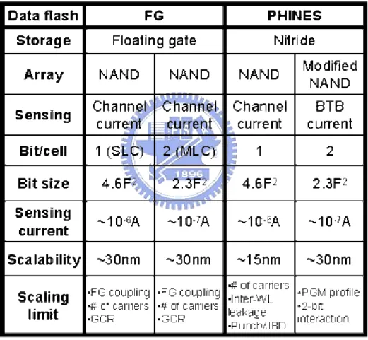
(9) Chapter 5 . Programmable Resistor with Erase-less Non-Volatile Memory (PREM) for SOC and Embedded Flash Applications 74 5.1 Introduction 74 5.2 Cell Structure and Characteristics 74 . . 5.3 PREM Array Architecture 5.4 Disturbances and Cell Retention 5.5 Scalability and Applications . . . . . 76 77 77 . . 5.6 Conclusion . . . . . 77 . Chapter 6 . A novel Silicon-Nitride based Light-Emitting Transistor (SiNLET) for Display and Optical Communications 96 6.1 Introduction 96 6.2 SiNLET Device Structure and Operation Principles 96 6.3 Electrical and Optical Properties 97 6.4 Conclusion 98 . . Chapter 7 Conclusion References Vita Publication List . . . . . . . . . vii. . . . . . . . . 112 114 121 123 .
(10) Table Captions Chapter 1 Table 1.1. NOR and NAND technology roadmap in ITRS 2002.. 6. Table 1.2. Summary of emerging non-volatile memories.. 7. Table 1.3. Operation bias conditions of a NROM cell.. 8. Chapter 2 Table 2.1 Table 2.2. Table 2.3. Key PHINES cell parameters. 19 Physical mechanisms and bias conditions of PHINES operation. Please refer to Fig.2.1 for the corresponding terminals and Bit-1 and Bit-2 in a PHINES cell. 21 The electrical performance of a PHINES cell. The Vt window in the table denotes the initial operation window, which does not include the charge loss, read disturbance, and other reliability margins.. 33. Chapter 4 Table 4.1. The comparison table of PHINES and floating gate technologies.. 73. Chapter 5 Table 5.1 Table 5.2. PREM cell parameters and program/read bias conditions. Summary of embedded memory cells.. 81 95. Chapter 6 Table 6.1. Summary of various test-bias conditions and test-device structures in Fig.6.4 and Fig.6.5. 103. viii.
(11) Figure Captions Chapter 1 Fig.1.1 Fig.1.2 Fig.1.3 Fig.1.4 Fig.1.5 Fig.1.6. Fig.1.7 Fig.1.8 Chapter 2 Fig.2.1 Fig.2.2 Fig.2.3 Fig.2.4. Fig.2.5. Fig.2.6 Fig.2.7. Fig.2.8. Major applications of flash memories (refer to Web Feet Inc. 2003). 5 Forecast of memory market share (refer to Web Feet Inc. 2003). 5 The cell structure of a floating gate flash memory cell. 6 The cell structure of a nitride storage flash memory cell. 7 Schematic representation of a NROM cell with physically 2-bits storage. The shaded area in the nitride layer represents stored charges.8 Schematic representation of the chip architecture with embedded flash memory array, high voltage periphery control circuit, and low voltage logic circuit. 9 Illustration of application and insertion of optical interconnections. 9 Illustration of integration of CMOS and silicon optical devices. 10. Schematic representation of the PHINES cell structure. 18 The array architecture of the test single cell. 18 TEM pictures of a PHINES cell along (a) Y-Y’ and (b) X-X’ (refer to Fig.2.2). 19 Schematic representation of the storage charges in a PHINES cell (top) and the channel surface potential (bottom) with two-bit storage. (a) Bit-1 and Bit-2 in erased states. (b) Bit-1 in a programmed state and Bit-2 in an erased state. (c) Bit-1 in an erased state and Bit-2 in a programmed state. (d) Bit-1 and Bit-2 in programmed states. 20 Negative FN erase characteristics of a PHINES cell. Threshold voltage (Vt) is defined as the applied gate voltage at which the drain current is 1µAmp. 22 Schematic representation of the band structure and the electrical field during negative FN injection in PHINES erase operation. 23 Programming characteristics of a PHINES cell. (a) Bit-1 is programmed to a low Vt while bit-2 is maintained at a high Vt. (b) Bit-2 is programmed to a low Vt while bit-1 is maintained at a low Vt. 24 IV characteristics of 3 cell states (both bits are erased, one bit is programmed and the other bit is erased, both bits are programmed). Solid line represents the IV of Bit-1 and dash line represents the IV of Bit-2. The cells are fresh cells. 25 ix.
(12) Fig.2.9. Fig.2.10. Fig.2.11 Fig.2.12. Fig.2.13. Fig.2.14 Fig.2.15. Fig.2.16 Fig.2.17 Fig.2.18. The measured charge pumping current (Icp) versus the high-level gate pulse (Vgh). The low level gate pulse is –4V. The open circles and solid circles represent the initial and erased state conditions, respectively. The solid up-triangles and down-triangles represent the charge distribution in nitride after 1µs and 200µs programming, respectively. 26 (a) The program characteristics of a PHINES cell. Condition A shows that two bits are both in high Vt states. Condition B shows that bit-1 is in a low Vt state and bit-2 is in a high Vt state. (b) Illustration of the channel potential in bit-1 read (condition A). (c) Illustration of the channel potential in bit-2 read (condition A). (d) Illustration of the channel potential in bit-1 read (condition B). (e) Illustration of the channel potential in bit-2 read (condition B). 27 Definitions and descriptions of the simulated cell parameters. 28 Simulated length of the residual electron distribution versus read Vd and Vt window with a programmed hole distribution of 60nm. Open symbols represent the minimum required Vd for the 0.8V Vt window and solid symbols represent the window with a read drain bias of 1.3V. 29 Simulated Vt windows versus the length of the programmed hole distribution with various electron densities and a residual electron distribution of 40nm. 30 Endurance behavior of 1-bit-per-cell operation. 31 Endurance behavior of 2-bits-per-cell operation. The cycle is repeated by erase => bit-1 program => bit-2 program. Circles represent that both bits are in high Vt states. Up-triangles represent that bit-1 is in a low Vt state and bit-2 is in a high Vt state. Down-triangles represent that both bits are in low Vt states. 32 Data retention (Vt loss) of three program/erase states. The storage temperature is 150C. The cells are 10K P/E cycled. 34 The temperature effect on data retention in high Vt states. The cells are 10K P/E cycled. 35 Effects of electron injection methods on the charge loss at the storage temperature of 150C. After stress of Vg=-24V for 1000s, two devices are conditioned to high Vt states (Vt=5V) by two electron injection methods and Vt shift is measured. Two electron injection methods are FN (Vg=-8V, Vb=10V) injection and SHE injection (Vg=2V, Vs=Vd=0V, VPWELL=-6V, VNWELL=-7V). 36 x.
(13) Fig.2.19. Fig.2.20. Fig.2.21 Fig.2.22 Fig.2.23 Fig.2.24 Fig.2.25. Chapter 3 Fig.3.1. Fig.3.2 Fig.3.3. Fig.3.4 Fig.3.5 Fig.3.6 Fig.3.7. Fig.3.8 Fig.3.9. (a) Illustration of the band structure in the hot electron injection condition. (b) Illustration of the band structure during the storage condition after the hot electron injection. 37 (a) Illustration of the band structure in Fowler-Nordheim injection condition. (b) Illustration of the band structure during the storage condition after Fowler-Nordheim injection. 37 Read disturbance characteristics of a PHINES cell. 38 PHINES (a) erase, (b) program, and (c) read operations in a virtual ground (NOR-type) array architecture. 39 The program behavior of cell-A and the disturbance behavior of cell-B and cell-C. 40 The simulated channel potential of cell-A and cell-B. 41 PHINES (a) erase, (b) program, and (c) read operations in a NAND-type array architecture. 42. Schematic representations of PHINES cell operations. (a) 2 bits are erased by FN electron injection. (b) Bit-1 is programmed by BTBT HH injection. (c) Bit-1 is read via sensing the BTB current. Bit-2 can be programmed and sensed by interchanging the role of the source and the drain. 47 Two-bits-per-cell erasing characteristics. 48 Two-bits-per-cell programming characteristics. (a) Bit-1 is programmed while Bit-2 is in an erased state. (b) Bit-2 is sequentially programmed while Bit-1 is in a programmed state. 49 Band structures of (a) BTB-PHINES program operation and (b) BTB-PHINES read operation. 50 Simulated read current in different channel lengths. 51 Schematic representation of BTB sensing scheme in the virtual ground array. 52 (a) The modified NAND-type array architecture and the operation conditions. (b) The cross sectional schematics of the array and the erase operation. (c) The cross sectional schematics of the array and the program operation. (d) The cross sectional schematics of the array and the read operation. 53 The program characteristics in three different gate lengths. 54 The IV characteristics in three different gate lengths. 55. xi.
(14) Fig.3.10 Fig.3.11 Fig.3.12 Fig.3.13 Fig.3.14. Chapter 4 Fig.4.1 Fig.4.2 Fig.4.3 Fig.4.4 Fig.4.5 Fig.4.6. Fig.4.7. Fig.4.8. Fig.4.9 Fig.4.10. The temperature dependence of the read current in 1 cycled and 10K cycled cells. 56 The cell endurance of 2-bits-per-cell operation. 57 The cell retention characteristics of 1-cycled and 10K-cycled cells. The storage temperature is 150C. 58 The read disturbance characteristics of the non-selected cells that serve as the pass transistors (Vg=10V or 12V, Vs=Vd=0). 59 The read disturbance characteristics of the selected cells (Vg/Vd/Vs= -10/2/F). One-cycled and 10K-cycled cells are compared. 60. Storage conditions of a 1-bit PHINES memory cell: (a) erased state, and (b) programmed state. 64 The NAND-type array architecture and bias conditions of 1-bit PHINES operation with channel current sensing scheme. 64 Number of storage carriers in a 1-bit PHINES cell. 65 Cross sectional representation of PHINES cells arranged in NAND-type array. 66 The paths of punch leakage current in (a) a NOR-type and (b) a NAND type array during the program operation. 66 The simulated punch leakage current in (a) a NOR-type and (b) a NAND type array during the program operation. In our calculations, there are 64 parallel WLs and leakage paths within one BL in a NOR-type array in our calculation. Two junction depths are also compared. Solid symbols and open symbols represent the junction depth of 0.1um and 0.03um, respectively. 67 The simulated punch leakage current in a NAND-type array during the program operation. Two junction depths (0.1um and 0.03um) and two bias conditions (Vd/Vs/Vg=5/0/-5 and 5/0/-10) are compared. 68 Schematic representations of the charge distribution in the 2-bits-per-cell PHINES operation: (a) long channel device with isolated two programmed bits and (b) short channel device with coupled two programmed bits. 69 Charge pumping characteristics of a PHINES cell. 70 (a) The 2-bit interaction ratio of a PHINES cell with BTB sensing scheme. (b) Illustration of 2-bit interaction in BTB sensing scheme. Electrons in bit-2 (erased state) will increase the BTB current of the programmed bit-1 in a scaled device. 71 xii.
(15) Fig.4.11. Chapter 5 Fig.5.1 Fig.5.2 Fig.5.3 Fig.5.4. Fig.5.5 Fig.5.6. Fig.5.7 Fig.5.8 Fig.5.9. Fig.5.10 Fig.5.11. Number of storage carriers per bit in a 2-bit PHINES memory cell with BTB sensing scheme. 72. (a) The breakdown behavior of a MIS diode with a 2.2nm oxide. (b) The breakdown behavior of a MIS diode with a 1.4nm oxide. 78 Illustration of the PREM cell structure. 79 The IV characteristics of a fresh and a programmed cell (Vg=1.3V). 79 The program voltage dependence of the read current evolution in PREM cells. Four program voltages are compared: VWL/VBL=2.4V /-2.4V, 2.2V/-2.2V, 2.0V/-2.0V and 1.8V/-1.8V. 80 MLC program algorithm of a PREM cell. 82 An exemplary illustration of a PREM cell to realize MLC operation. (a) 2-bits-per-cell storage. (b) 3-bits-per-cell storage. (c) 4-bits-per-cell storage. MTP program algorithm of a PREM cell.. 83 84. Illustration of cell distributions in (a) the 1st, (b) the 2nd, and (c) the 3rd program sequence. 85 An exemplary illustration of a PREM cell to realize MTP. (a), (b), and (c) represent the schematic representations of the 1st, the 2nd, and the 3rd time program (PGM) operations. Ref-1, ref-2, and ref-3 are the reference currents for each time program operation. 86 An exemplary illustration of a PREM cell to realize MTP+MLC (2-bits-per-cell storage with at least 5 programming times). 87 Schematic representations of (a) PREM array architecture and (b) 2. Fig.5.12. Fig.5.13. Fig.5.14 Fig.5.15. Fig.5.16. PREM cell structure. As small as 4F /cell is feasible. 88 (a) The array program condition and distribution of selected device A, non-selected device B and non-selected device C, and the single cell bias condition of (b) device A, (c) device B, and (d) device C. 89 (a) The array read condition and distribution of selected device A, non-selected device B and non-selected device C and the single cell bias condition of (b) device A, (c) device B, and (d) device C. 90 The program disturbance characteristics of (a) device B, and (b) device C at the temperature of 25C. 91 The read disturbance characteristics of four programmed levels. The disturbance condition is VWL/VBL=1.3V/0V at the temperature of 25C. 92 The cell retention characteristics of three programmed levels. The bake xiii.
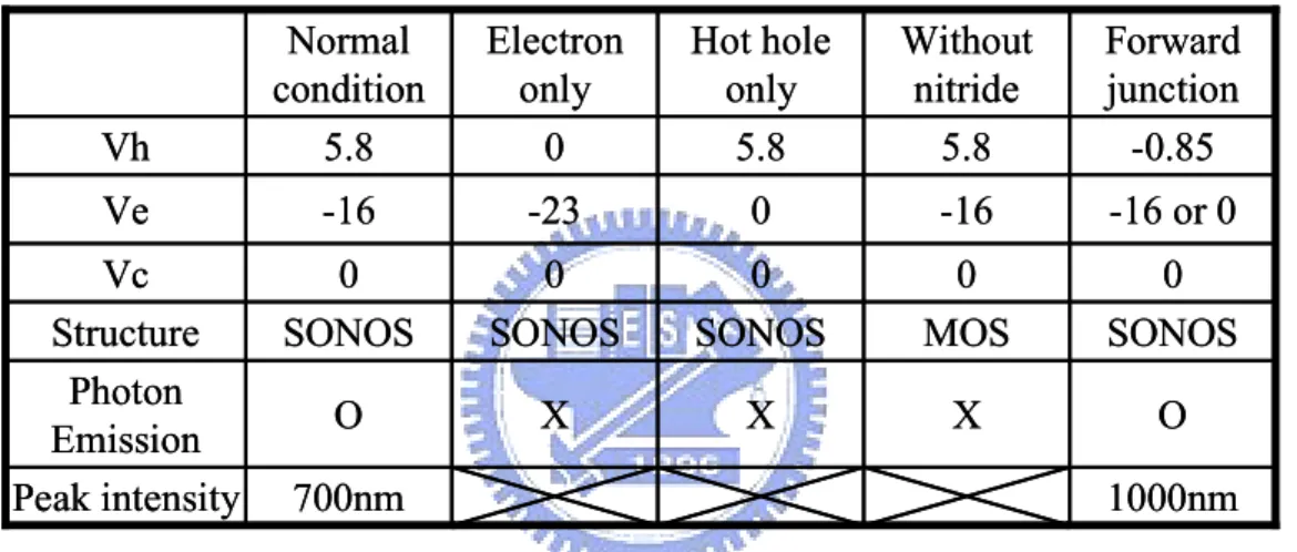
(16) Fig.5.17 Fig.5.18. Chapter 6 Fig.6.1 Fig.6.2 Fig.6.3 Fig.6.4. Fig.6.5. Fig.6.6. Fig.6.7. temperature is 150C. 93 The program behavior of two PREM cells with 1.4nm and 1.2nm oxide films. 94 The illustration of logic circuits with embedded SRAM and PREM for SOC applications. 95. The device structure of SiNLET. ONO thickness is 9, 7, and 6nm from top to down. 99 Layout of SiNLET test device. 99 Schematic representation of the band diagram of SiNLET in the operation condition of light emission. 100 (a) Light spectrums of various bias conditions and device structures. Squares represent the spectrum of the normal operation condition of SiNLET. Circles and up-triangles represent the spectrum with FN-E supply only and BTBT-HH supply only in SONOS structure, respectively. Down-triangles represent the spectrum of the normal operation condition in MOS structure (oxide thickness is 18nm). (b) CCD image of SiNLET in the normal operation condition. (c) CCD image of MOS structure in the normal operation condition (Vc/Ve/Vh=0/-16/5.8). 101 Light spectrum of SiNLET in the operation condition of forwardbiased junction (circles) and reverse-biased junction (squares). Reverse-biased junction shows shorter wavelength and higher photon energy, and the supply current is 3 orders less than the forward-biased junction. 102 (a) Light spectrum of SiNLET in various Ve (Vh=5.8V). Higher Ve shows larger intensity. The peak intensity is at 700~800nm in all conditions. (b) The supply current (Ih) versus the operation voltage of poly (Ve) with a constant Vh of 5.8V. In all bias conditions, the current at n+ junction is equal to p-well (Ih=Ic) and the current at the poly (Ie) is negligible. 104 (a) Light spectrum of SiNLET in various Vh (Ve=-16V). Higher Vh shows larger intensity. The peak intensity is at 600~700nm in all conditions. (b) The supply current (Ih) versus the operation voltage of n+ junction (Vh) with a constant Ve of -16V. In all bias conditions, the current at n+ junction is equal to p-well (Ih=Ic) and the current at the poly (Ie) is negligible.. 105 xiv.
(17) Fig.6.8. Fig.6.9 Fig.6.10 Fig.6.11 Fig.6.12. Fig.6.13. Schematic illustration of SiNLET to function as a three-terminal transistor. The poly supplying electrons serves as the “Drain”. The n+ junction supplying holes serves as the “Source”. The p-well controlling the lateral field serves as the “Gate”. The nitride traps serves as quantum dots for carrier trapping and recombination. 106 The supply current density versus output light intensity. The data are extracted from Fig.6.6 and Fig.6.7. 107 The light intensity as a function of Vc (Vh=5.8V, Ve=-16V). The threshold voltage of Vc is around 2V to switch SiNLET. 108 The light intensity as a function of Ve and Vh (Vc=0V). 109 The light spectrum before and after stress. The stress condition and light emission measurement condition are both Vc/Ve/Vh= 0/-16/5.8V. 110 Illustration of integration of CMOS and SiNLET devices. 111. xv.
(18) Chapter 1 Introduction 1.1 An Overview of Mass Storage Flash Memory Technologies Today, flash memory has come of age as a mainstream memory product, and its technologies and markets will become more diversified. It can be classified into two major markets: code storage application and data storage application (see Fig.1.1). NOR-type flash memory [1.1] is most suitable for code storage application, such as cellular phone, PC bios, and DVD player. NAND-type flash memory [1.2] has been targeted at data storage market, which is an emerging application such as PDA, memory cards, multi-media audio, and digital still camera. Fig.1.2 discloses the memory market, and flash memory share increased rapidly in the last few years. Conventional NOR-type and NAND-type flash memories use the same floating gate structure as shown in Fig.1.3. Table 1.1 shows the ITRS roadmap [1.3] for flash memory cells. NOR-type flash memory cell has good visibility into 90nm and 65nm generation. Current projection shows that scaling continues at 45nm node but is challenged to meet the goal of 50% cell size shrinkage [1.1,1.4]. NOR-type flash memory has two scaling limiters. One is the non-scalability of tunnel oxide and inter-poly ONO due to reliability concerns. The other is caused by the channel hot electron programming, which requires an internal voltage of more than 8V, and imposes the limit of the cell gate length [1.4]. Besides, the process complexity increases dramatically to shrink the memory cell size, which makes the cost ineffective. NAND-type flash memory cell meets another scaling limitation caused by floating gate interference. Vt shift is caused by the Vt change and capacitive coupling of the adjacent cells. It is very likely that the practical limit of NAND-type flash memory is at 30nm technology node [1.5]. Instead of the process scaling, one important innovation in cost reduction is multi-level cell (MLC) operation. Although MLC operation can double the memory density [1.6], scaling limitations of conventional floating gate memory cell mentioned above are coming in the near future. Accordingly, several new memory concepts are under investigating to maintain Mooreís law as shown in Table 1.2. Nitride trapping storage flash memory [1.7] and nano-crystal flash memory [1.8] are evolutionary approaches, and their processes are compatible to the standard CMOS process. FeRAM [1.9], MRAM [1.10], PRAM [1.11], and Polymer [1.12] memory architectures are revolutionary approaches with new materials. Although many efforts and resources have been devoted to develop these memory cells, most emerging . 1.
(19) memories still have reliability problems, and are not commercially available for fabricating yet except for the nitride trapping flash memory. 1.2 Introduction of SONOS Flash Memory Cell SONOS flash memory cell (Fowler-Nordheim tunnel program by electron and direct tunnel erase by hole [1.7]) has been proposed for years. As shown in Fig.1.4, the carriers are stored in the traps of the nitride layer between the top and the bottom oxides. SONOS cell offers several advantages over conventional floating gate memory cells: simple process, ease of manufacturing, no erratic bit, not sensitive to oxide defects, and no floating gate coupling effect. However, the cell retention is an issue due to the thin bottom oxide. Besides, its large cell size (6F2) and slow program/erase speed limit its applications. Recently, SONOS cell has evolved into a 2-bits-per-cell storage architecture (NROM [1.13]) by utilizing the localized charge trapping effect of nitride. Localized trapping nitride trapping storage memory cell enables a memory cell to hold twice as much data as the standard memory cell, without compromising device endurance, performance or reliability. NROM flash memory cell structure is shown in Fig.1.5, and the operation principle is shown in Table 1.3. NROM programs its memory cell by channel hot electron injection as conventional NOR-type floating gate memory does, which is suitable for code storage applications. Erase is done by band-to-band tunneling induced hot-hole injection. A novel ì reverse read schemeî [1.13] is introduced to realize physically 2-bits-per-cell operation. NROM holds 2 physical bits in one cell above the source and drain junction, which is more reliable alternative to MLC solutions in the floating gate memory cell. MLC products suffer from performance and reliability concerns when detecting between multiple charge levels. Although NROM cell has many advantages over conventional floating gate memory cells, it can only be applied to code storage application due to its high power consumption and slow program speed in program operation. Previous works [1.14-1.15] reveal that reliability issues including read disturb, over erasure and cell retention after cycling are major challenges. Besides, 2-bit interaction effect resulted from the reverse read scheme also limits the device scalability [1.16]. In this dissertation, we construct a novel nitride trapping storage memory cell. The memory cell does not suffer 2-bit interaction issue and shows great performance for the candidate of next generation flash memory technology. 1.3 Introduction of Embedded Flash Memory Technologies The requests for high performance system combining CMOS devices and embedded flash memories have increased for SOC applications (smart cards, cellular . 2.
(20) communications, automotiveÖ ). However, the integration of CMOS devices and conventional floating gate flash memories shows difficulties in terms of complex process and high cost. Besides, high periphery voltages, large current pumper, and high voltage transistors are necessary to operation the memory cell, which will consume active area, complicate the process, and increase die cost as shown in Fig.1.6. Although several memory cells [1.17-1.19] have been proposed for embedded applications, the device scalability and/or cell reliability are still issues. These memory devices also face scaling challenges due to the non-scalable gate stack for the consideration of cell retention. Therefore, the development of a high performance memory cell with non-volatility, low voltage operation, good reliability, high-density storage, good scalability, and simple process (CMOS compatible) is essential for embedded markets. In this dissertation, we report a novel embedded flash memory cell and its process is compatible to CMOS devices. The memory performance and array architecture are discussed. 1.4 Introduction of Light Emitting Devices Electrical wires meet a fundamental limitation of aspect ratio, and capacitive coupling, which reduces the bit rate. Below 0.13um, interconnect delay starts to dominate over gate delay in Si CMOS. The scaling limitations of electrical wires give an opportunity for optical interconnects. Optical interconnection avoids the issue of aspect ratio. They can replace global wires to provide high data rates. III-V based optical devices are widely accepted due to its direct bandgap and high photon emission efficiency. Silicon is not considered as a good light-emitting source due to its indirect bandgap induced low emission efficiency. Although silicon optical devices suffer lower light emission efficiency, their applications are numerous (see Fig.1.7) due to the ease of integration in CMOS-based ultralarge scale integrated circuit (ULSI) as shown in Fig.1.8. Silicon light emitting devices can also be used in massively parallel optical interconnects and cross connects for microprocessor and digital-signal processor applications. Traditionally, silicon LEDs have been regarded as a difficult candidate for light emission since they suffer low light emitting efficiency due to the indirect band-gap of silicon. Recently, many attempts including p-n diodes [1.21], MIS diodes [1.22], and nanocrystal LEDs [1.23] have shown that light emission from silicon materials is readily obtained. 1.5 Organization of this Dissertation In this dissertation, a novel PHINES (Programming by hot Hole Injection Nitride Electron Storage) flash memory cell is investigated. PHINES uses the nitride storage cell structure. PHINES cell, with its superior reliability, 2 bits-per-cell storage and low . 3.
(21) power operation, can meet the need of both code and data storage applications. Chapter 2 will discuss the cell structure, operation principles, array architecture, and reliability characteristics. In chapter 3, a novel BTB sensing scheme and a new modified NAND-type array are introduced to eliminate the issue of 2-bit interaction. Chapter 4 discusses the scaling challenges of PHINES memory cell. In chapter 5, we construct another novel non-volatile flash memory cell named Programmable Resistor with Erase-less Non-Volatile Memory (PREM). PREM can realize multi-time programming, multi-level cell operation, non-volatility, and low voltage operation, and can meet some applications in SOC and embedded areas. In chapter 6, we develop a novel Silicon-Nitride based Light-Emitting Transistor (SiNLET) with high light emission efficiency, low current consumption and a small device area. The fabrication process of SiNLET is compatible to CMOS technology. SiNLET demonstrates its high feasibility for the application of optical interconnects in ULSI. Finally, a conclusion will be given in chapter 7. . 4.
(22) Function. Application. Data. MP3. CAMERAS. NAND Networking. Code+Data. DVD STB. Mobile. Industrial. Code+Parameter PC Modem. Code Only. NOR. Automotive. HDD.Add-on boards,CDROM. Printer,DVD,PDA OA,Games,TV. . . 20. FLASH. 15. 10. SRAM 5. 0. 1996. 1998. 2000. 2002. 2004. 2006. 2008. Fig.1.2 Forecast of memory market share (refer to Web Feet Inc. 2003). . . . . Market(B$). Fig.1.1 Major applications of flash memories (refer to Web Feet Inc. 2003). Semiconductor Memory Market 30 25 DRAM . 5.
(23) . Poly gate. . ONO Floating gate Oxide. . S. D. Fig.1.3 The cell structure of a floating gate flash memory cell. . Table 1.1 NOR and NAND technology roadmap in ITRS 2002. Year. 2001 2004. 2010 2013. Technology node (nm). 130. 90. 65. 50. 35. Cell Size (F2). 10. 10. 11 ~14. 12 ~15. 13 ~16. NOR. NAND. Cell Size 0.16 0.081 0.053 0.034 0.018 (µm2) Cell Size (F2). 5.5. 5.5. 4.5. 4.5. 4.5. Cell Size 0.093 0.045 0.019 0.011 0.006 (µm2). . 2007. 6.
(24) . Table 1.2 Summary of emerging non-volatile memories.. Transistor Vt shifts 1.Floating gate 2.Nitride trap 3.Nano-crystal. Charge Displacements 1.Crystalline Ferroelectric 2.Polymer Ferroelectric. 1.Magnetic: GMR or MJT 2.Phase Change 3.Polymer ionic transport. Poly gate Oxide Nitride Oxide S. D. Fig.1.4 The cell structure of a nitride storage flash memory cell. . . Resistance Change. 7.
(25) . bit2. bit1. Fig.1.5 Schematic representation of a NROM cell with physically 2-bits storage. The shaded area in the nitride layer represents stored charges. . Table 1.3 Operation bias conditions of a NROM cell. . Bit 1. Bit 2. Program. Erase. Read. Vg. 11V. -3V. 2.5V. Vd. 5V. 8V. 0V. Vs Vg. 0V 11V. 0V -3V. >1.5V 2.5V. Vd. 0V. 0V. >1.5V. Vs. 5V. 8V. 0V. . 8.
(26) . Flash Memory Array . HV periphery LV logic/SRAM. Fig.1.6 Schematic representation of the chip architecture with embedded flash memory array, high voltage periphery control circuit, and low voltage logic circuit. Chip to chip optical interconnects Chip to system optical interconnects. SRAM/DRAM. ïSensor ïDetector ïReceiver. A/D switch. Controller. Processor 1. ì. î. Flash/NVM. Chip to system optical interconnects. I/O. ïInterface ïHuman ïMachine. Processor 2. Denotes potential paths of optical interconnects.. Fig.1.7 Illustration of applications and insertion of optical interconnections. . . 9.
(27) . hν. Optical device. CMOS. Fig.1.8 Illustration of integration of CMOS and silicon optical devices. . . . 10.
(28) Chapter 2 PHINES Flash Memory Cell with Low Power Program/Erase, Backward-Read Scheme and 2-bit-per-cell Storage 2.1 Introduction Interest in nitride based localized trapping storage flash memory cells has revived for 2-bits-per-cell operation, which can double the memory density [2.1-2.3]. Besides, they also show better scalability since charges are stored in the nitride traps rather than a poly-silicon floating gate in conventional flash memory cells. Nitride storage memories do not have floating gate induced drain turn-on and coupling issues that are believed to be the scaling limitations of conventional floating gate memories [2.4,2.5]. Various operation schemes were proposed based on the nitride-storage cell structure. SONOS flash memory with modified Fowler-Nordheim-tunneling programming by electrons and direct-tunneling erasing by holes was proposed long time ago [2.6]. The absence of erratic bits and low power operation make SONOS a good candidate for next generation flash technology. However, the cell retention is still an issue now [2.7]. Besides, its large cell size (6F2 per bit [6]) and slow program/erase speed limits its applications. Recently, NROM cell with channel-hot-electron (CHE) programming and band-to-band tunneling induced hot-hole (BTBT HH) erasing [2.2] has demonstrated excellent intrinsic cell performance. NROM cell is suitable for code flash applications, and CHE programming is widely accepted in NOR-type architecture. In spite of many advantages, previous works [2.8-2.13] reveal that reliability issues including read disturb, over erase, and cell retention after cycling are major challenges of NROM cell. C.T. Swift et al proposed to use uniform tunneling for erasing [2.3] instead of the hot-hole injection to reduce the stress of high energetic holes in the erase operation. However, for mass storage and data flash applications, CHE programming is still not suitable due to its high power consumption. Here, a novel flash memory cell named PHINES (Programming by hot Hole Injection Nitride Electron Storage) [2.1] is investigated. PHINES uses the nitride storage cell structure and can be arranged in both NOR-type and NAND-type array for code and data flash applications. The operation principles, cell characteristics, and cell reliability will be studied and characterized in this chapter. 2.2 PHINES Cell Structure PHINES memory cell is a NMOSFET with an ONO stack as the gate dielectric . 11.
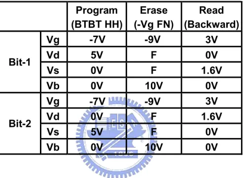
(29) (Fig.2.1). The test single cell is arranged in a virtual-ground array as shown in Fig.2.2, which is free of field isolation. The key cell parameters are listed in Table 2.1. The gate length and gate width are 0.19µm and 0.14µm, respectively. The thickness of each ONO layer is 9nm, 6nm, and 6nm from top to bottom. The top oxide and bottom oxide are formed by thermal oxidation while nitride is performed by CVD deposition. A double poly technology, novel low-temperature dielectric film fill-in and planarization process is introduced to form a sufficiently thick insulating layer between the local buried-diffusion (BD) bit-lines and the word-lines (WLs) [2.14]. Figure 2.3 (a) and (b) show the TEM pictures of the cell, in which the X-pitch and Y-pitch are 0.33µm and 0.28µm, respectively. 2.3 PHINES Cell Operation Condition, and Cell Characteristics 2.3.1 PHINES Cell Operation Condition PHINES cell uses gate FN electron injection (negative gate-to-substrate bias) and BTBT HH injection as the erase and program methods, respectively. Schematic representations of PHINES cell operation are shown in Fig.2.4. The bias conditions are given in Table.2.2. Figure 2.5 shows the erasing characteristics and the Vt saturates after 1ms. As shown in Fig.2.6 (a), electrons are injected from the gate via tunneling through the top oxide (path 1) in the erase operation. Some of the tunnel electrons are captured by the nitride traps (path 2, either deep traps or shallow traps), while the others will inject into the substrate (path 3). Electrons in the shallow traps will easily be drawn out due to the high electric field (path 4) and only electrons in deep traps remain in the nitride. Accordingly, the erase saturation may be caused by the limited amount of deep nitride traps, and cell Vt will saturate while all deep traps are filled with electrons. PHINES cell does not have an over-erasure problem due to the self-convergent behavior of FN injection, which can improve the uniformity and tighten the Vt distribution of the erased cells. The program of a PHINES cell is done by lowering the local Vt through edge BTBT HH injection. Fig.2.6 (b) shows the band structure of PHINES cell during program operation. Figure 2.7 shows the program characteristics of the two bits. In Fig.2.7 (a), bit-1 is programmed to a low Vt, while bit-2 is in the erased state. Bit-2 is subsequently programmed in Fig.2.7 (b). Since the program is performed by bit-by-bit and shot-by-shot tracking, a verification step is applied after each program shot to well control the program behavior of each bit. The program of each bit stops as its Vt or current passes the program verification. Over-program induced leakage current in the low Vt state between two columns can be suppressed, and a narrow Vt distribution of the program cells can be achieved. Read of PHINES cell is performed by a . 12.
(30) backward-read scheme as shown in Table 2.2. To read bit-1 (bit-2), a source (drain) bias is applied to reduce the channel potential near bit-2 (bit-1). The IV characteristics of each state are shown in Fig.2.8. 2.3.2 The Charge Distribution In Fig.2.9, the charge pumping technique [2.15] is utilized to monitor the charge variation in the nitride. The open circles and solid circles represent the initial and erased conditions. The Vt shift after erase is around 2.5V. The solid up-triangles and down-triangles represent the charge distribution in nitride after 1µs and 200µs programming. After FN electron erasing and hot-hole programming, a tail of charge pumping current (Icp) is observed. The turn-on Vt (Vgh) of the Icp tail is proportional to the number of storage holes in a programmed bit while the amount of the Icp tail is proportional to the length of the programmed holes in the channel region. As program time increases, the increase of Icp in the portion of 1V<Vgh<3.5V represents that hot holes are injected into the nitride from junction edge toward channel wherein a bit is programmed. 2.3.3 2-bit Interaction Effect Two-bit interaction effect is a unique phenomenon in physical 2-bit storage memory cell, which is caused by the interaction between bit-1 and bit-2 during backward read operation. Similar to NROM cell [2.16], PHINES cell suffers 2-bit interaction effect and operation Vt window reduction due to the channel current sensing and the backward read scheme. Fig.2.10 (a) shows the program characteristics. In the initial state (condition A), two bits are in high Vt states. Figure 2.10 (b) and (c) illustrate the channel potential of condition A during read operation. As bit-1 is intentionally programmed to a low Vt state, a slight Vt decrease is observed in bit-2 (condition B in Fig.2.10 (a)), which induces Vt window reduction. Fig.2.10 (d) and (e) illustrate the channel potential of condition B (bit-1 is in a low Vt state while bit-2 is in a high Vt state). In condition B, as bit-1 is read (see Fig.2.10 (d)), a high read Vd is used to pull down the channel potential near bit-2, and a low Vt of bit-1 is thus sensed. To read bit-2 (see Fig.2.10 (e)), the high read Vd and the local/narrow electron distribution of bit-2 after bit-1 programming will enhance the Drain-Induced-Barrier- Lowering (DIBL) effect and lower the channel potential. Compared to the condition A (Fig.2.10 (c)), a lower Vt of bit-2 is obtained, and a reduced Vt operation window is caused. Since the Vt of bit-2 is very sensitive to the programmed condition of bit-1, we name this phenomenon ì 2-bit interaction effectî . Device simulation is used to characterize the effects of cell parameters on the Vt operation window. The definitions of the simulated cell parameters are descried in . 13.
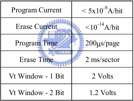
(31) Fig.2.11. As shown in Fig.2.12 and Fig.2.13, three parameters will dominate the Vt window of a PHINES cell: read Vd, the length of the residual electron distribution, and the density of the stored electrons. In Fig.2.12, as the length of the residual electron distribution decreases (the length of the programmed hole distribution increases), Vt window increases under a fixed read Vd and, in other words, read Vd can be reduced to maintain a constant Vt window. Besides, higher stored electron density can also increase Vt window without increasing the read bias as shown in Fig.2.13. A narrower electron distribution, a higher electron density, and a lower read Vd could suppress the DIBL effect enhanced Vt reduction and enlarge the Vt window. Accordingly, 2-bit interaction effect can be suppressed by optimizing the charge profiles and the operation schemes. As mentioned in Section 2.3.1, PHINES can determine the stored electrons via erase operation and well control the injected amount of holes to modulate the length of residual electrons via program and program verification, separately. Although we can suppress Vt window reduction via better operation algorithms and carrier injection processes to manage the charge distribution, the 2-bit interaction effect cannot be eliminated completely in the backward read scheme. Besides, 2-bit interaction effect will get worse in the next generation due to the enhanced DIBL in a scaled device. In chapter 3, a novel BTB-PHINES memory cell and BTB-sensing (band-to-band sensing) scheme are developed to solve this issue completely. 2.3.4 PHINES Cell Endurance and Vt Operation Window Figure 2.14 and Fig. 2.15 show the P/E cycling endurance of 1-bit-per-cell and 2-bits-per-cell operation, respectively. The Vt window is almost unchanged up to 10K P/E cycles. A slight window closure is observed after 100K cycles. This phenomenon is widely observed in flash memory cells, which should result from the stress-induced bottom/top oxide degradation [2.17]. The Vt operation window of 1-bit-per-cell and 2-bit-per-cell operation is around 2V and 1.2V, respectively. 2.3.4 PHINES Cell Performance The electrical performance of a PHINES cell is summarized in Table 2.3. Program can be finished within 200µs and erase can be done in 2ms. Vt-windows of 2V and 1.2V are obtained for 1-bit-per-cell and 2-bits-per-cell operation. Since the program current is less than 50nA/bit, high programming rate can be achieved by parallel programming. Besides, FN-erase also consumes extremely low current (10fA/cell). Both program and erase are low power operations, which makes it suitable for mass storage (data flash) applications. . 14.
數據
相關文件
Large data: if solving linear systems is needed, use iterative (e.g., CG) instead of direct methods Feature correlation: methods working on some variables at a time (e.g.,
Threads are assigned to processors by the scheduler for executions. Each processes have their own memory (for
電機工程學系暨研究所( EE ) 光電工程學研究所(GIPO) 電信工程學研究所(GICE) 電子工程學研究所(GIEE) 資訊工程學系暨研究所(CS IE )
此位址致能包括啟動代表列與行暫存器的 位址。兩階段的使用RAS與CAS設定可以
[r]
雙極性接面電晶體(bipolar junction transistor, BJT) 場效電晶體(field effect transistor, FET).
原因: 技術進步,加上對可攜帶音樂設備的需求增加(黑膠唱片 > 錄音帶 > CD- ROM > 迷你光碟 > SD咭 >
下列關於 CPU 的敘述,何者正確?(A)暫存器是 CPU 內部的記憶體(B)CPU 內部快取記憶體使 用 Flash Memory(C)具有 32 條控制匯流排排線的 CPU,最大定址空間為
