國 立 交 通 大 學
電子工程學系 電子研究所碩士班
碩 士 論 文
碳離子佈植對鎳化矽熱穩定性與碳化矽形
成影響之研究
Effects of Carbon Ion Implantation on NiSi
Thermal Stability and Si-C Formation
研 究 生:羅子歆
指導教授:崔秉鉞 博士
碳離子佈植對鎳化矽熱穩定性與碳化矽形成
影響之研究
Effects of Carbon Ion Implantation on NiSi
Thermal Stability and Si-C Formation
研究生:羅子歆 Student:Tzu-Hsin Luo
指導教授:崔秉鉞博士 Advisor:Dr. Bing-Yue Tsui
國立交通大學
電子工程學系 電子研究所碩士班
碩士論文
A Thesis
Submitted to Department of Electronics Engineering and Institute of Electronics College of Electrical and Computer Engineering
National Chiao Tung University in Partial Fulfillment of the Requirements
for the Degree of Master in
Electronic Engineering July 2010
Hsinchu, Taiwan, Republic of China
i
碳離子佈植對鎳化矽熱穩定性與碳化矽形成影響之研究
研究生:羅子歆 指導教授:崔秉鉞 博士
國立交通大學
電子工程學系 電子研究所碩士班
摘要
本篇論文中,我們使用電漿浸潤式碳離子佈植(CPIII)與低溫碳離子佈植兩種 製程作為碳離子佈植的方式。分別將此兩種碳離子佈植技術應用於兩個方向,分 別為改善矽晶圓表面形成之鎳化矽薄膜之熱穩定性以及在碳離子佈植入矽晶圓 以後經後續之退火製程形成碳化矽。 在 CPIII 的研究上,首先我們發現在經過 CPIII 製程之後,N+P 接面的漏電 並沒有明顯增加,此結果減少了我們對 CPIII 可能傷害 N+ P 接面的疑慮。在經過 一分鐘能量 5keV 的 CPIII 製程之後,未經砷參雜的 NiSi 薄膜之結塊溫度可以上 升到 800℃,但經過砷參雜之後的試片, CPIII 並沒有增加熱穩定性的效果。我 們也發現 CPIII 在製程中會在表面沉積一層碳薄膜,若離子佈植過程後剩餘的碳 膜太厚,將會影響 NiSi 的形成。CPIII 應用在碳化矽形成上的結果較不理想,佈 植時間五分鐘能量 3keV 之 CPIII 製程的試片在做過 650℃120 秒鐘的退火之後, 在替代位置上的碳原子百分濃度僅有 0.301%,這是因為 CPIII 在製程中所形成的 表面非晶層過少且非晶程度低的緣故。 低溫碳離子佈植的好處是能夠在表面形成厚且非晶程度高的非晶層,在載台 溫度 15℃下經過能量 7keV 劑量 5×1015 cm-2 碳離子佈植的試片具有約 49 奈米接 近完全非晶化的非晶層。碳離子佈植也被發現可以使矽基板中的磷離子在經過退 火之後的分佈變的比退火之前淺,此項特性有助於實現超淺接面結構。在增加ii NiSi 熱穩定性上,低溫碳離子的表現和 CPIII 類似,對於經過磷離子佈植的試片 低溫碳離子佈植並不能增加 NiSi 的熱穩定性。在碳化矽形成的應用上,低溫碳 離子佈植因為能夠形成非晶程度高且後的非晶層而具有優勢。我們針對離子佈植 的能量、劑量及載台溫度上的不同分別進行實驗後,發現佈植能量 7keV 劑量 5×1015 cm-2為較佳的佈植條件。而當載台溫度介於 5℃與 15℃之間時,其對退火 後在替代位置上的碳原子濃度影響不明顯。我們也針對碳化矽形成所需的退火製 程條件如第一階段退火的溫度及秒數和第二階段退火的方式進行實驗。在實驗結 果中可發現第一階段退火的條件以溫度 750℃時間 120 秒較佳,過高的溫度或過 久的秒數反會使替代位置上的碳原子濃度降低。第二階段的退火的溫度需要很高 以增加在過飽和狀態下的固態溶解度,但退火的時間需遠低於 1 秒,否則亦會使 替代位置上的碳原子濃度降低。雷射退火因為其單一脈衝的退火時間僅 25 奈秒, 故為一種十分具有潛力的第二階段退火方式。綜合以上各項理想的製程參數,我 們使用載台溫度-15℃,佈植能量 7keV 劑量 5×1015 cm-2的試片,在經過第一階 段退火溫度 750℃時間 120 秒及第二階段能量 350 mj/cm2,五個脈衝的雷射退火 後,替代位置上的碳原子濃度可以達到 1.091%。
iii
Effects of Carbon Ion Implantation on NiSi Thermal
Stability and Si-C Formation
Student: Tzu-Hsin Luo Advisor: Dr. Bing-Yue Tsui
Department of Electronics Engineering and Institute of Electronics
National Chiao Tung University
Abstract
In this thesis, we use carbon plasma immersion ion implantation (CPIII) and low temperature carbon ion implantation as carbon implantation source. We applied the two processes on the application of increase NiSi thermal stability and Si-C formation.
On the research of CPIII, first we find the leakage current of N+P junction after CPIII
process didn’t increase. This result is beneficial for application on junction structure. After CPIII at 5 keV for 1 minute, the agglomeration temperature of NiSi thin film without arsenic doping could increase to 800 ℃. But on the arsenic doped sample, CPIII could not increase NiSi thermal stability. We also find CPIII will deposit a carbon thin film on the surface during process, if the carbon film is too thick after all ion implantation process, it will affect the formation of NiSi. The result of CPIII application on Si-C formation is not ideal, the substitutional carbon density of sample that performed CPIII at 3 keV for 5 minutes then annealing at 650 ℃ for 120 sec is only 0.301 %. That is because the surface amorphous layer produced by CPIII is not thick enough and the level of amorphous is low.
The benefit of low temperature carbon ion implantation is it can produce thick amorphous layer with high amorphous level after process. After implantation at 7kev with a dose of 5×1015 cm-2 on a -15℃ chuck, the surface amorphous layer is about 49 nm and is near totally amorphous. We also find the implanted phosphorous profile after annealing would be shallower than the profile of as-implanted sample. This
iv
characteristic is beneficial for application on ultra-shallow junction fabrication. On the NiSi thermal stability application, we find low temperature carbon ion implantation could not improve thermal stability of phosphorous implanted NiSi film, which is similar to CPIII. We find low temperature carbon ion implantation is promising on Si-C formation application because it can produce thick and high quality surface amorphous layer after process. We perform low temperature carbon ion implantation with different energy、dose and chuck temperature and try to find the ideal implantation condition. From the result we find implantation energy at 7keV with a dose of 5×1015 cm-2 is the most ideal condition. We also try different annealing condition including first step annealing temperature、time and second step annealing method to find the ideal annealing condition. For first step annealing, temperature at 750 ℃ for 120 sec is the ideal condition. If the temperature is too high or the time is toolong, the density of substitutional carbon would decrease. Second step annealing time should be very high to increase carbon solid state solubility in silicon under supersatuation state, but the annealing duration time should be much shorter than 1 sec or the substitutional carbon density will decrease, too. The time duration of PLA is only about 25 ns for each shot, which is a promising second step annealing technique. Finally, by combine the optimized process condition, sample implanted at 7keV with a dose of 5×1015 cm-2 on a -15℃ chuck after first step annealing at 750 ℃ for 120 second and second step annealing using PLA at energy 350 mj/cm2 for 5 shots, the substitutional carbon density can reach 1.091%.
v
謝誌
能夠順利完成碩士班的學業,首先最要感謝的就是我的指導老師 崔秉鉞教 授。從大學四年級開始跟著老師做專題,老師在學術研究上面追根究底且一絲不 苟的精神,讓我了解甚麼才是正確的研究態度及學術倫理。在私底下,老師熱心 公益及正直的性格,更是我學習的典範。 接著要感謝實驗室的學長姐,李振銘、盧季霈、謝志民、王俊凱、賴瑞堯、 蔡依成以及余昆武在機台使用上給我的訓練以及實驗結果上的討論。有你們為我 執點迷津,我的實驗才能夠順利完成;感謝實驗室的夥伴們 李勃學、周智超以 及顏志展,在這兩年裏面,我們一起分享了很多無論是實驗上或是生活上的酸甜 苦辣,也時常為彼此加油打氣。很開心,我們真的做到了;謝謝學弟們鄭嶸健、 王培宇以及陳璽允協助處理實驗室的事務,讓我們沒有後顧之憂。 感謝漢辰科技公司的陳恆綱博士以及原能會核能所的蔡文發博士,提供我離 子佈植的設備讓實驗能夠順利的進行。你們在實驗條件上提供的專業意見以及對 於實驗結果的討論都讓我受益匪淺。 謝謝我大學時期以及國中時期的好朋友們。雖然這兩年大家不能很常見面, 但每一次的小聚跟閒暇時的聊天都讓我能夠紓解自己的情緒跟壓力,有你們真 好。 感謝我的女朋友嘉珮,這兩年來無論在快樂的時候或者是難過失落的時候, 我的身邊都有妳的陪伴,妳的體貼與支持是我最大的動力。 最後也是最重要的,要感謝我的父母親 羅纘綺先生、官淑珍女士。感謝你 們從小對我的栽培還有在這些年裡面源源不絕付出的關愛。還有弟弟 羅子澄的 分享及意見替我排解了很多心事跟壓力。我真的是個很幸運的人,因為有你們的 存在。 最後,我要把這篇論文獻給所有我感謝的人。vi
Contents
Abstract (in Chinese)……….……….……….….……i
Abstract (in English) …..………..……….….……iii
Acknowledgement………v
Contents………...………….……vi
Table Captions…...………..….……….…viii
Figure Captions………...……….……….…..ix
Chapter 1 Introduction
1.1 Why Using Carbon Implantation Process……….1
1.2 Improve Nickel Silicide Thermal Stability by Carbon Implantation…2
1.3 Source/Drain Stressor Formation by Carbon Implantation…………...4
1.4 CPIII and Low Temperature Ion Implantation………..6
1.5 The Organization of this Thesis………9
Chapter 2 Experimental Procedure
2.1 Carbon Ion Implantation Method………...15
2.2 Sample and Device Fabrication………..16
vii
Chapter 3 Carbon Plasma Immersion Ion Implantation
3.1 Introduction………27
3.2 Basic Material Analysis of CPIII on Si Substrate…………...……...27
3.3 CPIII Junction Analysis………..28
3.4 Impact of CPIII on NiSi/Si Structure……….32
3.5 Si-C Forming by Using CPIII……….37
Chapter 4 Low Temperature Carbon Ion Implantation
4.1 Introduction………59
4.2 Basic Material Analysis………..59
4.3 Thermal Stability of NiSi/Si Structure………...62
4.4 Si-C Formation………...64
Chapter 5 Conclusion
5.1 Summary………..………...93
5.2 Future Work………95
viii
Table Captions
Chapter 1 Introduction
Table 1-1 The comparison of standard characteristic between NiSi and NiSi2…...11
Table 1-2 The comparison between Source & Drain Si-C stressor forming by CVD and by Carbon ion implantation………..11
Chapter 3 Carbon Plasma Immersion Ion Implantation
Table.3-1 The reverse bias leakage current of junction with a DC bias 3V under different CPIII condition and annealing condition (N+P)……….39 Table.3-2 The ideal factor of junction under different CPIII condition and
annealing condition (N+P)………39
Chapter 4 Low Temperature Carbon Ion Implantation
Table.4-1 The sheet resistance value of carbon implanted silicon substrate after Si-C formation (Ⅰ)………...73 Table.4-2 The sheet resistance value of carbon implanted silicon substrate after
Si-C formation (Ⅱ).………..73 Table.4-3 The sheet resistance value of carbon implanted silicon substrate after
ix
Figure Captions
Chapter 1 Introduction
Fig.1-1 The difference on stressor material and stress direction between PMOSFET and NMOSFET………12 Fig.1-2 The strain component produced by SiC/Si heterojunction………...13 Fig.1-3 The schematic diagram of PIII system……….14
Chapter 2 Experimental Procedure
Fig.2-1 The process environment and equipment of PIII……….21 Fig.2-2 The control panel of process chamber valves………...22 Fig.2-3 The DC power supply of electrical power system………22 Fig.2-4 The DC high voltage power supply of electrical power system…………...23 Fig.2-5 The process flow of junction fabrication………..24
Chapter 3 Carbon Plasma Immersion Ion Implantation
Fig.3-1 SIMS depth profile after CPIII process (10keV/15min)………...40 Fig.3-2 SIMS depth profile after CPIII process (3keV/5min)………...40 Fig.3-3 The TEM image of 3keV/5min CPIII sample………..…41 Fig.3-4 Leakage current analysis of different CPIII condition (650℃120secs
anneal)………..……42 Fig.3-5 Leakage current analysis of different CPIII condition (650℃120secs 1st step anneal and 800℃30secs 2nd step anneal)……….42 Fig.3-6 Leakage current analysis of different annealing condition (3keV1min)...43 Fig.3-7 Leakage current analysis of different annealing condition (3keV5min)…..43
x
Fig.3-8 Leakage current analysis of different annealing condition (5keV1min)…..44 Fig.3-9 Leakage current analysis of different annealing condition (5keV5min)…..44 Fig.3-10 The sheet resistance value of pure NiSi sample with annealing temperature
500℃ to 900℃, annealing time 30secs………...45 Fig.3-11 The SEM images of pure NiSi sample with annealing temperature 500℃ to 900℃, annealing time 30secs………46 Fig.3-12 The XRD patterns of pure NiSi sample with annealing temperature 500℃ to 900℃, annealing time 30secs………...47 Fig.3-13 The sheet resistance value of 3keV1min and 5keV1min CPIII samples
with annealing temperature 500℃ to 900℃, annealing time 30secs. (No As)………...…47 Fig.3-14 The XRD patterns of 3keV1min CPIII NiSi samples with annealing
temperature 500℃ to 900℃, annealing time 30secs. (No As)………...48 Fig.3-15 The SEM images of 3keV1min CPIII NiSi samples with annealing
temperature 500℃ to 900℃, annealing time 30secs. (No As)………...49 Fig.3-16 The XRD patterns of 5keV1min CPIII NiSi samples with annealing
temperature 500℃ to 900℃, annealing time 30secs. (No As)………...50 Fig.3-17 The SEM images of 3keV1min CPIII NiSi samples with annealing
temperature 500℃ to 900℃, annealing time 30secs. (No As)………...51 Fig.3-18 The sheet resistance value of implant energy 3keV and 5keV implant time
1min and 5mins CPIII and pure NiSi samples with annealing temperature 500℃ to 900℃, annealing time 30secs. (with As)……….52 Fig.3-19 The SEM images of 3keV1min CPIII NiSi samples with annealing
temperature 500℃ to 900℃, annealing time 30secs. (With As)………53 Fig.3-20 The SEM images of 5keV1min CPIII NiSi samples with annealing
temperature 500℃ to 900℃, annealing time 30secs. (With As)………54 Fig.3-21 The SEM images of 3keV5min CPIII NiSi samples with annealing
temperature 500℃ to 900℃, annealing time 30secs. (With As)………55 Fig.3-22 The SEM images of 5keV5min CPIII NiSi samples with annealing
xi
temperature 500℃ to 900℃, annealing time 30secs. (With As)………56 Fig.3-23 The XRD patterns of 5keV5min CPIII NiSi samples with annealing
temperature 500℃ to 900℃, annealing time 30secs. (With As)………57 Fig.3-24 The XRD rocking curve patterns of 3keV5min CPIII NiSi samples with
annealing temperature 650℃ and 750℃, annealing time 120secs. (With As)………..58
Chapter 4 Low Temperature Carbon Ion Implantation
Fig.4-1 SIMS depth profile after 7keV/-15℃/5×1015 cm-2 low temperature carbon ion implantation (as-implanted)………...75 Fig.4-2 SIMS depth profile after 7keV/-15℃/5×1015 cm-2low temperature carbon ion
implantation (750℃/120secs annealed)………...76 Fig.4-3 SIMS depth profile of phosphorous before and after 750 ℃ /120secs annealing………..77 Fig.4-4 The TEM image of 7keV/5×1015 cm-2 low temperature (5℃ ) carbon
implanted sample……….78 Fig.4-5 The TEM image of 7keV/5×1015 cm-2 low temperature (-15℃) carbon
implanted sample……….79 Fig.4-6 The TEM image of 7keV/5×1015 cm-2 low temperature (-15℃) carbon
implanted sample after annealing at 750℃ for 120 sec………..80 Fig.4-7 The sheet resistance value of implant energy 3keV and 5keV low
temperature carbon implant and pure NiSi samples with annealing temperature 500℃ to 900℃, annealing time 30secs. (with P)………81 Fig.4-8 The SEM images of 3keV/5×1015 cm-2 low temperature (5℃) carbon
implantation NiSi samples with annealing temperature 500℃ to 900℃, annealing time 30secs. (with P)………...82 Fig.4-9 The SEM images of 5keV/5×1015 cm-2 low temperature (5℃) carbon
implantation NiSi samples with annealing temperature 500℃ to 900℃, annealing time 30secs. (with P)………...83 Fig.4-10 The XRD rocking curve patterns of low temperature carbon implant
xii
samples, with 5℃ chuck temperature at a dose of 5×1015 cm-2 . The implant energy ranged from 3keV to 7keV. The samples were annealed with temperature 700℃for 120secs……….84 Fig.4-11 The XRD rocking curve patterns of low temperature carbon implant
samples, with -15℃ chuck temperature at a dose of 5×1015 cm-2 . The implant energy ranged from 7keV to 9keV. The samples were annealed with temperature 750℃for 120secs……….85
Fig.4-12 The XRD rocking curve patterns of low temperature carbon implant samples, with -15℃ chuck temperature and 7keV implant energy. The dose was 5×1015 cm-2 and 8×1015 cm-2. The samples were annealed with temperature 750℃for 120secs………..86 Fig.4-13 The XRD rocking curve patterns of low temperature carbon implant
samples, with 7keV implant energy at a dose of 5×1015 cm-2. Chuck temperature is 5 ℃ and -15 ℃ .The samples were annealed with temperature 750℃for 120secs………..87 Fig.4-14 The XRD rocking curve patterns of low temperature carbon implant
samples, with 7keV implant energy at a dose of 5×1015 cm-2. Chuck temperature is 5℃. The samples were annealed with temperature 650℃ to 850℃ for 120secs……….88 Fig.4-15 The XRD rocking curve patterns of low temperature carbon implant
samples, with 7keV implant energy at a dose of 5×1015 cm-2. Chuck temperature is -15℃. The samples were annealed with temperature 750℃ for 90secs to 180secs……….89 Fig.4-16 The XRD rocking curve patterns of low temperature carbon implant
samples, with 7keV implant energy at a dose of 5×1015 cm-2. Chuck temperature was 5 ℃ . The samples were annealed with first step temperature annealing 750℃ for 120secs, and one of the sample were performed 1000℃ second step annealing for 1 second………...90
xiii
Fig.4-17 The XRD rocking curve patterns of low temperature carbon implant samples, with 7keV implant energy at a dose of 5×1015 cm-2. Chuck temperature was 5 ℃ . The samples were annealed with first step temperature annealing 750℃ for 120secs, and one of the sample were performed PLA second step anneal at energy 350mj/cm2, number of shots is 5……….91 Fig.4-18 The XRD rocking curve patterns of low temperature carbon implant
sample (3keV/5×1015 cm-2/5 ℃ ) and CPIII sample (3keV/5min). The samples were annealed with temperature 650℃for 120secs……….92
1
Chapter 1
Introduction
1.1 Why Using Carbon Ion Implantation Process
CMOS technology is the predominant technology in very large scale integrated circuits now. Willing to approach the benefits like high device density, high operation speed, low power consumption, and low cost, scaling down has become the most important topic in CMOS technology for decades. As the device shrinks beyond 32nm technology node, scaling down becomes more challenging and difficult. It requires new materials and new processes to overcome those physical limitations imposed by the traditional ones.
Carbon is known to be one of the consequential elements in silicon wafers. To reduce the negative impacts brought by carbon, the carbon density in silicon wafers is demanded to be lower than 1ppm in silicon device manufacturing processes for a long time. From the late 1980s, several benefits of carbon ion implantation in silicon substrate have been found in some researches. The first benefit is the carbon atoms in silicon substrate can getter metal atoms like Au and Cu effectively, thus reduce the leakage current brought by metal contamination and improve the yield in IC production. According to the research of H. Wong et al., the amounts of gettered Au by 1×1016 cm-2 of carbon ion implantation is 5×1013 cm-2 which is higher than the Au atoms which were gettered by oxygen (2.3×1012 cm-2), nitrogen (4×1012 cm-2), and BF2(4×1012 cm-2) ion implantation [1]. The second benefit is the carbon atoms in the
substitutional site of silicon substrate can capture interstitial silicon atoms effectively, and reduce the secondary defects caused by ion implantation processes which will
2
increase junction leakage current [2, 3], and improve the performance of devices. Furthermore, interstitial silicon is also one of the main reasons of why Transient Enhanced Diffusion (TED) happens in the junction area. Ultra-shallow junction is an important demand to avoid short channel effect in CMOS technology. But even by using low energy ion implantation technique to implant the dopants extremely close to the surface, the dopant distribution will be broadened by TED during the dopant activation process. By incorporating carbon into substitutional site, carbon can reduce the TED effect by capture of interstitial silicons, and help to realize ultra-shallow junction at source and drain area [4, 5].
Recently, another two important applications of carbon ion implantation process have been developed. They are using carbon ion implantation to improve the thermal stability of nickel silicide and implanting carbon into source and drain area to form silicon carbide as stressor [6~10]. The stressor can increase electron mobility in n-channel MOSFET, and improve device performance. These two applications are the main topics of this thesis, and the background and current status will be explained in the following sections.
1.2 Improve Nickel Silicide Thermal Stability by
Carbon Implantation
As MOSFETs scale down, comes by the increase of the parasitic resistance of the source and drain area. This issue will limit the turn-on current of MOSFETs. In order to reduce the series parasitic resistance, the salicide (self-aligned metal silicide) process technique has been used in high performance ICs since 1980s. Beyond 90nm process node, nickel becomes the standard material for salicide process. Comparing to
3
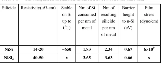
the other kind of metal silicides, nickel silicide has several benefits like low resistivity, low temperature process, less silicon consumption during silicide formation, and no narrow line effect and bridge effect [11]. Although there are many benefits for nickel silicide, there is a major drawback. It is about the thermal stability issue. When the process temperature is high, the agglomeration of nickel silicide will happen. Agglomeration will make the nickel silicide film un-continuous and increase the value of sheet resistance. High process temperature will also induce the nickel silicide phase transformation from NiSi to NiSi2. There are two main drawbacks of NiSi2, the first
one is the silicon consumption during NiSi2 formation is twice of the silicon
consumption during NiSi formation. Second, we can see in Table 1-1 that the resistivity of NiSi2 is higher than the resistivity of NiSi. If phase transformation
occurs the sheet resistance will increase. Thus, raising the thermal stability of nickel
silicide becomes the main subject for realizing NiSi contact structure. In 2004, S. Zaima et al. found that when Ni film deposited on P+-Si0.996C0.004, the
agglomeration temperature and phase transform temperature will both increase [6]. V. Machkaoutsan et al. reported that as the number of substitutional carbon increases, the thermal stability of nickel silicide will be better [7]. In summary, high density of carbon in silicon substrate can improve the thermal stability of nickel silicide significantly.
On the application of SiC stressor, in early stage, most researches use Low Pressure Chemical Vapor Deposition (LPCVD) technique to epitaxially grow Si1-xCx
layer on silicon substrate. The drawbacks of LPCVD SiC technique are the expensive cost of the process, low throughput, and non-repeatable process performance [9]. Recently, some research found that carbon ion implantation is a simpler and low cost technique to form Si1-xCx layer on silicon substrate [8~10]. And the number of carbon
4
atoms in silicon substrate is easier to be controlled by ion implantation compared to the LPCVD method. Low energy carbon ion implantation can make most of the implanted carbon near the Ni/Si surface, it is expected that improvement of thermal stability can be achieved. Table.1-2 compares the difference between Si-C formation by CVD and carbon implantation method.
1.3 Source/Drain Stressor Formation by Carbon
Implantation
Scaling is a useful solution to increase device speed and integrated circuit density. As scaling becomes more and more difficult, another solution to increase device performance is necessary. Improving channel carrier mobility by source and drain stressor is one of the solutions which have been applied in recent years. By using different materials to form stressor on the source and drain area, it can provide tensile or compressive strain to the channel. Using materials like SiGe [12~16] and compressive SiN liner [17, 18] as source and drain stressor can provide compressive stress to the channel, it will increase hole mobility and reduce electron mobility so that it is used on P-MOSFET. On the other hand, using SiC or tensile SiN liner [19~23] as source and drain stressor can provide tensile stress to the channel, it will increase electron mobility and reduce hole mobility so that it is used on N-MOSFET. Figure 1-1 shows the difference in stressor materials and stress directions between P-MOSFET and N-MOSFET.
As has been mentioned, SiC source and drain stressor is a promising approach to increase N-MOSFET channel mobility. The Si1-xCx has a relaxed lattice constant
5
constant of single crystal silicon. When a Si1-xCx layer is grown on Si, the Si1-xCx
lattice is compressed vertically and stretched horizontally. In that way, the lattice constant of SiC on the growth direction is further decreased. The value is [25], where and is the stiffness constants. Figure1-2 shows that the smaller vertical lattice of Si1-xCx interacts
with the adjacent Si lattice, it will induce a lateral tensile stress to the channel [26]. The stress will contribute to electron mobility increase and improve N-MOSFET performance.
Many research found that the number of (atomic percentage of the substitutional carbon in Si lattice) is an important factor that effects the enhancement of electron mobility induce by the SiC stressor. To increase the Csub value becomes
the main topic to improve the Si-C Source & Drain stressor process. Using LPCVD to growth epitaxial SiC is one of the methods to form the Source & Drain Si-C stressor. In the research of T. Y. Liow et.al, the Csub can achieve 2.3% by using LPCVD
method [27]. Although high value can be achieved by LPCVD method, it still has several drawbacks like low throughput and non-repeatable process performance [9]. And, the Source & Drain recess process before stressor growth increases the cost and complexity of the device process.
Carbon ion implantation has been applied to Si-C source & drain stressor formation process recently. The benefit of carbon ion implantation is that it only needs two process steps, carbon ion implantation and thermal solid-phase epitaxial (SPE) treatment, to form SiC stressor. The source & drain recess process is not in need. This advantage makes carbon ion implantation a cost-effective and simpler process for Si-C stressor forming. Carbon ion implantation also has some advantages such as high throughput and it can suppress the TED effect of dopants to realize
6
ultra-shallow junctions. The value that a process can produce is controlled by two important factors: the thickness and amorphous level of the surface amorphous layer after carbon ion implantation [9]. When monomer implantation is used, the carbon ion isn’t heavy enough to form a totally amorphized layer on the Si surface. Ge PAI (Germanium pre-amorphous implantation) is suggested to be integrated with monomer Carbon carbon ion implantation to form the SiC stressor [10]. Ge ion implantation before carbon ion implantation can produce an amorphous layer on the Si surface, compensates the drawback of monomer carbon ion implantation. In the work of N. Nishikawa et.al, by using Ge PAI and monomer carbon ion implantation, the can be raised to 1% after SPE annealing [10]. Although the Ge PAI process can produce good quality amorphous layer on the Si surface, it will make the process more complex and increase the cost. Cluster-carbon ion implantation process is another method to form SiC stressor, it uses + as ion source instead of monomer carbon ion. Since + has heavy mass, cluster-carbon ion implantation process has
self-amorphizing capability, it can produce amorphous layer on the Si surface without extra PAI process. In the research of S. M. Koh et.al, by using cluster-carbon ion implant and proper anneal treatment can fabricate a SiC stressor which has a density of 1.1% [11].
1.4 CPIII and Low Temperature Ion Implantation
As mentioned in the previous section, carbon ion implantation has several promising applications in semiconductor device fabrication. But there are still some short comes on the traditional carbon ion implantation technique like it could not create a good quality amorphous layer with only monomer carbon ion implantation. The other short come is the traditional type of ion implanter could not provide implant energy lower than 20keV. It makes the carbons can only locate at deeper region of the
7
silicon substrate, and makes no benefit to the device structure at the surface region of the substrate. Plasma immersion ion implantation (PIII) and low temperature ion implantation are two kinds of ion implantation technique which can overcome the short comes of the traditional ion implantation, and were used as carbon implantation technique in this thesis. These two techniques are described specifically in the following paragraphs.
1. Plasma Immersion Ion Implantation (PIII)
Plasma immersion ion implantation is a surface deposition technique, which applies high voltage pulsed DC or pure DC power to extract the accelerated ions from the plasma and targeting the ions into the wafer placed on the sample holder. Fig1-3 is the schematic diagram of a PIII system, the holder is in a vacuum chamber which is connected to a high voltage power supply and insulated from the chamber wall. When the process begins, the substrate is applied with a negative bias, the electric field drives electrons away from the substrate and forms a Debye sheath layer. The Debye sheath layer contains only positive ion and no electrons in it. The biased substrate will accelerate the ions in the Debye sheath layer and implant the ions into the wafer on the holder.
The benefit of PIII process is that the implantation energy is controlled by the voltage of the pulsed DC signal, so the dopants can be implanted into the shallow region of the object surface by very low implantation energy. And because the object is totally immersed in the plasma, so PIII can implant high density of dopants into the wafer in a relatively short time compare to traditional ion implanter. In that way, the throughput of implantation process can be increase.
Several applications of PIII has been implemented by researchers. Using nitrogen PIII process to improve the surface property of stainless steel is one of the applications. By performing NPIII process, the surface hardness of stainless steel can
8
be improved [28, 29]. Another important application is performing oxygen PIII on the metallic biomaterials which are used on medical purposes such as osteosynthesis plates used in jaw or skull surgery. After OPIII treatment, the biocompatibility of the biomaterials will be improved [30~34]. Diamond like carbon (DLC) film forming is another application of PIII [35~37]. The DLC film has a high hardness and Young’s modulous, a good wear and abrasion resistance and a low friction coefficient. So it can be used in semi-conducting, biomedical, automotive and aerospace industries. And PIII is a promising way of efficiently forming DLC film on object’s surface. PIII has several applications on semiconductor device fabrication. First, because PIII can do low energy ion implantation, it can be used on ultra-shallow junction fabrication. In the research of C.A. Pico et al., PMOS is successfully fabricated by using BPIII process [38]. PIII is also used on sidewall doping of trench structure [39]. Since PIII has immersion type doping characteristic, the sidewall doping of high aspect ratio trench structure is easier by using PIII. Nitrogen PIII can use on suppress thermal hillock formation in aluminum metallization [40], or improve the electrical characteristics of high-k gated MOS devices [41].
In this thesis, we used carbon PIII process to implant high density and low energy carbon ions into the shallow region of the Si substrate. Considering the benefits of PIII mentioned in the previous paragraphs, PIII might be a promising technique to do Carbon implant on silicon substrate in our expectation.
2. Low Temperature Ion Implantation
The amorphous layer thickness and the level of amorphization are the two most important factors to affect the number of substitutional carbon atoms. Using traditional ion implanter to do carbon ion implantation with the chuck at room temperature or higher temperature is not easy to produce an amorphous layer with
9
enough thickness and amorphous level. For that reason, it needs Ge PAI process before traditional carbon ion implantation and will increase the cost and complexity of the process [42].
Low temperature ion implantation has been developed for several years. By putting wafer on a low temperature chuck, the temperature of the target wafer is lower than that in the traditional ion implanter. Low temperature wafer contains less thermal energy than high temperature wafer, in this way the effect of self-anneal mechanism during carbon implantation could be reduced [43]. This phenomenon is benefit for SiC stressor formation because it helps to produce thicker and higher amorphization level amorphous layer, which helps to increase the number of substitutional carbon atoms.
1.5 The Organization of this Thesis
The organization of this thesis is described below. Chapter 1 introduce the applications of carbon implantation and raises the main topics of this thesis - using carbon implantation to improve NiSi thermal stability and to form SiC Sourse & Drain stressor precisely. Chapter 2 describes the process procedure of sample preparation and device fabrication, and the electrical and material analysis methods. The carbon implantation techniques are also introduced. Chapter 3 describes how carbon implantation affects the NiSi thermal stability. The agglomeration effect and phase transformation effect are both included. The electrical characteristics of the n+-p junctions with carbon incorporation are also discussed in this chapter. Chapter 4 illustrates how the annealing condition and carbon implantation condition affects the
10
11
Table 1-1 The comparison of standard characteristic between NiSi and NiSi2
Silicide Resistivity(μΩ-cm) Stable on Si up to (℃) Nm of Si consumed per nm of metal Nm of resulting silicide per nm of metal Barrier height to n-Si (eV) Film stress (dyne/cm) NiSi 14-20 ~650 1.83 2.34 0.67 6×10⁹ NiSi2 40-50 x 3.65 3.63 0.66 x
Table 1-2 The comparison between Source & Drain Si-C stressor forming by CVD and by Carbon ion implantation
CVD Carbon
Implantation
Recess etching requirement
Need S/D recess etch No S/D recess etch Process performance reproducibility Non-repeatable process performance Repeatable process performance Surface amorphous layer
requirement
No surface amorphous layer requirement
Require surface amorphous layer
Process throughput low high
Process complexity complex easy
Process cost high lower
Existence of interstitial Carbon Yes Yes
12
Fig.1-1 The difference on stressor material and stress direction between P-MOSFET and N MOSFET
13
Fig.1-2 The strain component produced by SiC/Si heterojunction
14
Fig.1-3 The schematic diagram of PIII system
15
Chapter 2
Experimental Procedure
2.1 Carbon Ion Implantation Methods
2.1-1.Carbon Plasma Immersion Ion Implantation (CPIII)
The PIII system used in this thesis consists of process chamber, electrical power system, vacuum system, and gas providing system. Fig.2-1 shows the whole PIII equipment. The process chamber is a chamber with sample chuck at the bottom and an antenna to light the plasma on. A valve control panel is linked to the chamber to control all the valves linked to the process chamber. Fig.2-2 shows the control panel of the valves. Fig.2-3 and Fig.2-4 show the electrical power system, it includes a DC power supply and a DC pulse signal source. The vacuum system includes two pumps and one pressure meter. One pump is for the first step vacuum to make the pressure down from air pressure, the other pump is a turbo pump which can make the chamber pressure down to 10-6 torr. The gas providing system includes CH4 gas source and a
gas flow meter.
At the beginning of the process, we put the wafer on the sample chuck. Then we use the vacuum system to make the chamber pressure down to 10-5 torr. After the process pressure reached, CH4 gas is pour into the process chamber with a flow rate of
50 sccm. DC power supply is turned on to light on the plasma with a value of 150V. In the final step, DC pulse signal is applied to the chuck and the carbon ions are implanted into the silicon substrate, the process pressure is about 1.2 × 10⁻³ torr.
2.1-2. Low Temperature Ion Implantation
The low temperature ion implanter used in this thesis is model iPulsar produced by Advance Ion Beam Technology Co. (AIBT). The allowed implantation energy range is 100 eV – 40 keV and the dose range is 1x10¹³ to 5x10¹⁶ ions/cm2. Tilt angle
16
is from 0˚ to 45˚ and the twist angle is from 0˚ to 360˚. Since the implanter is an equipment designed for 12-inch wafer process, we use a 12-inch wafer as wafer holder, and attach 6-inch wafer on it, then put the holder on the chuck to perform ion implantation.
The iPulsar system contains one focused ion beam 2D mechanical scan system and one uniform strip shape ion beam 1D mechanical scan system, can provide various kind of implantation, especially low energy ion implantation. The cold wafer e-chuck in the iPulsar system is a special equipment, and is one of the major differences compare to conventional ion implanters. During the process, the chiller is flowed through the e-chuck and makes the chuck temperature low, the lowest temperature that e-chuck could achieve is -20 ℃. The backside gas flow between the wafer backside and chuck is controlled to conduct the heat. Low temperature e-chuck can lower the temperature of wafer, and can provide several process benefits. Those benefits will be discussed in the following chapter.
2.2 Sample and Device Fabrication
2.2-1.Nickel Silicide Thermal Stability Sample
Six-inch-diameter p-type (100) silicon wafers with nominal resistivity of 15~25 Ω-cm were used as substrates. The PIII was performed at 3 keV and 5 keV, and the implantation time is 1 min and 5 min. The samples are labeled in the form of xKyM, where the xK indicates the implantation energy is at x keV and the yM indicates the plasma immersion time is y min. After PIII, the 3K5M and 5K5M samples accepted additional arsenic ion implantation at 30 keV to a dose of 5×1015 cm-2. Then, all samples were dipped in diluted HF solution with (H2O:HF = 50:1) to remove the
17
system. The process pressure is 6×10⁻⁷ torr and the Ni deposition rate is 0.5A/sec. After Ni deposition, samples were cut into small pieces and were annealed in N2
ambient by a rapid thermal annealing (RTA) system at temperatures ranging from 500 ℃ to 900 ℃ for 30seconds. The unreacted Ni was selectively etched by a mixture of H2SO4 : H2O2=3:1.
2.2-2.Substitutional Carbon Density Sample
Six-inch-diameter p-type (100) silicon wafers with nominal resistivity of 15~25 Ω-cm were used as substrates. The low temperature ion implantation was performed at chuck temperature of 5℃ or -15℃. The implant energy is at 3 keV, 5 keV, 7 keV, and 9 keV. The implantation dose is controlled to 2~5×1015 cm-2. The implantation conditions of samples are labeled in the form of energy/dose. For the samples implanted at 5℃ chuck temperature the implantation conditions are 3 keV/5×1015 cm-2、5 keV/5×1015 cm-2 and 7 keV/5×1015 cm-2. For the samples implanted at -15℃ chuck temperature, the implantation conditions are 7 keV/5×1015 cm-2、7 keV/8×1015 cm-2、9 keV/5×1015 cm-2 and 3 keV/2×1015 cm-2+ 5 keV/3×1015 cm-2+ 7 keV/3×1015 cm-2. Then all the samples accepted additional phosphorous ion implantation at 17 keV to a dose of 5×1015 cm-2. After phosphorus ion implantation, the samples were cut into small pieces and two steps of annealing process were performed for SiC formation. In the first step, samples were annealed in N2 ambient by a rapid thermal
annealing (RTA) system at temperatures ranging from 650 ℃ to 850 ℃ for 90 to 180 secs. In the second step, some of the samples were annealed in N2 ambient by a RTA
system at temperature of 1000℃ for 1sec second. Some samples were annealed by a pulse laser annealing (PLA) system. A 248nm KrF excimer laser was used as laser source, the laser energy is 350 mJ/cm2, the pulse duration is around 25 ns/shot and the number of shots ranges from 5 to 20.
18
substitutional carbon density of the CPIII process. The carbon ion implant condition is 3K5M and the annealing temperature is 650℃ and 750℃ for 120 secs.
2.2-3.N
+P Junction Fabrication
In this experiment, the active region is defined by the typical LOCOS process. After active region definition, carbon was implanted followed by dopant implantation. Finally the junction structure was annealed at different annealing conditions. The detailed process steps are described as follows.
First, we use six inches p-type silicon wafer with nominal resistivity of 15~25Ω-cm as substrates. After RCA clean, we use horizontal furnace to grow dry oxide 35 nm and nitride 150 nm. Use lithography process to define active region. (No PR on the field oxide region), then TEL 5000 is used to remove the dry oxide and nitride on the field oxide region. After active region definition, PR is removed by Mattson asher, then dip SPM for 10 minutes to remove the residual PR. After dipped in SPM, 550 nm wet oxide is grown on the field oxide region by horizontal furnace, then dip hot H3PO4 for 60 minutes to remove nitride on active region then dip HF for
350 sec to remove pad oxide. Grow 35 nm wet oxide by horizontal furnace then use HF dip 350 sec to remove wet oxide, this step is used to avoid white ribbon effect. Use PIII to do Carbon implantation, the implantation condition is (energy/time) 3keV/1min、3keV/5min、5keV/1min、5keV/5min,some of the samples are without Carbon implantation, they are used as control samples. After CPIII process, do As implant at energy 30keV with a dose of 5×10¹⁵/cm2, which is the common condition of Source/Drain doping. After all implantation step, use AG610i to do 650℃~750℃ 120secs first step annealing, some of the samples do 800℃ 30secs second step annealing. The schematic diagram of this process is in Fig2-5.
19
2.3 Material Analysis and Electrical Measurement
Several Material Analysis techniques include XRD、SEM、SIMS and TEM were used in our experiment. Electrical measurement of blanket sample sheet resistance and the forward bias and reverse bias characteristics of CPIII junction structure were performed, too.
XRD analysis has two main purposes in this experiment. The first one is to find out the nickel silicide phase transformation temperature. The second purpose of XRD is to calculate the number of substitutional carbon by using the rocking curve method proposed by P. C. Kelires in 1997 [13]. This model can calculate the atomic percentage of the substitutional carbon in Si matrix (Csub) by the lattice constant
difference (Δd) obtained from the XRD rocking curve. The detail is introduces in the next paragraph. First, the lattice constant difference Δd between Si and Si1-xCx could
be obtained by the XRD rocking curve result. The lattice constant of Si1-xCx on the
growth direction a⊥ can be calculated by
(
After obtained the value of a⊥, the value of relaxed lattice parameter arel can be
calculated by
Finally the value x of Si1-xCx can be extracted by solving the following Equation
Scanning Electron Microscope (SEM) is used to inspect the surface morphology of the carbon implanted nickel silicide samples after annealing at different conditions. The surface continuity and the level of agglomeration can be observed by SEM inspection. Secondary Ion Mass Spectrometry (SIMS) is used to analysis the depth profiles of carbon and phosphorus atoms in samples after ion implantation and
20
annealing. Transmission Electron Microscopy (TEM) is used to observe the microstructure of samples. It can help to figure out the thickness of amorphous layer and the level of amorphization.
For electrical measurement, the sheet resistances of all blanket samples were measured by four point probe. The forward bias and reverse bias junction characteristics were measured by the semiconductor analyzer of model Agilent 4156C.
21
22
Fig.2-2 The control panel of process chamber valves
23
24
1. RCA clean.
2. Use horizontal furnace to grow dry oxide 350A and nitride 1500A.
3. Active region define by Lithography process.
4. TEL5000 dry etching
25
6. Growth 5000A wet oxide by horizontal furnace.
7. Use hot H3PO4 remove Si3N4, then use HF remove SiO2.
8. Growth 350A wet oxide by horizontal furnace, remove the oxide by HF dip. (Remove white ribbon effect)
26
9. Carbon implantation by PIII.
10. As+ implantation.
11. Annealing by RTA.
27
Chapter 3
Carbon Plasma Immersion Ion Implantation
3.1 Introduction
Plasma immersion ion implantation (PIII) is an ion implantation method which uses plasma as implantation source. Because the immersion type nature of plasma, PIII has the benefit of high throughput[44]. And because it’s implantation energy is provided by DC pulse signal, PIII can implant the dopants into the shallow region of the object with very low energy. PIII has been applied in several purpose like metal surface treatment、medical biomaterial surface treatment, and diamond like carbon (DLC) film forming on surface of object.
In this part of experiment, we use PIII as carbon ion implantation source. First, we discuss the basic characteristic of CPIII silicon substrate. Second, the electrical characteristics of the CPIII junction will be analyzed. Then the thermal stability improvement of CPIII NiSi/Si structure is discussed, both without N+ doping and with N+ doping samples are included. In the last part, silicon carbide (Si-C) forming of
CPIII samples is performed.
3.2 Basic Material Analyses of CPIII on Si Substrate
In this part, TEM was used to analyze the surface condition of the implanted silicon surface and SIMS was used to measure the depth profile of the carbon distribution after carbon plasma immersion ion implantation. Fig3-1 and Fig3-2 shows the SIMS result of the carbon implanted silicon substrate, we can find that if the implantation time is 15 minutes, the effective carbon dose could achieve 1.52×1018cm-2 and most of the implanted carbons are located in the top 50 nm from
28
the surface of the substrate. When the implantation time decreases to 5 minutes, the effective carbon dose is 2.515×1016cm-2 and the implanted carbons are mostly located at the region which is near the surface. Fig3-3 is the TEM result of 3K5M CPIII sample, we can see that there is a 32nm thick amorphous layer on the surface of silicon substrate.
Since too many carbon implanted into silicon will deactivate other dopants and increase the interface contact resistance [45]. The suitable carbon dose in the silicon substrate should be between 1×1015 cm-2 and 1×1016 cm-2. Base on all the experimental data, the carbon implantation time will be controlled less than 5 minutes in the following experiments, which is expected to produce better experimental results.
3.3 CPIII Junction Analysis
In this part, we perform reverse bias leakage current analysis and forward bias ideality factor analysis on the basic N+P junctions with carbon PIII process. This experiment can tell us the CPIII process will do harm to the junction electrical characteristic or not.
3.3-1.Reverse Bias Leakage Current
In this sub-section, we will discuss two main subjects. The first one is the impact on reverse bias leakage current brought by different implantation energies or times, under the same SPE annealing condition. And the second one is the impact on reverse bias leakage current brought by different SPE annealing conditions, under the same implantation energy and time.
29
From Fig 3-4 and Fig 3-5we can observe the reverse bias leakage current measurement results, we can find that the difference in leakage currents between different carbon implantation conditions is very small. The samples with 5keV implantation energy have slightly smaller leakage current in comparison with the samples with 3keV implantation energy under the same implantation time. Under the same implantation energy, the samples with 5 minutes carbon implantation have smaller leakage current than the samples with 3 minutes carbon implantation. Those leakage current differences are within one order of magnitude, which is not evident. We can also find that, although the process of carbon implantation may create some defects in the substrate, we can find that the leakage current of carbon implanted samples don’t have evident difference from control samples. In some implantation conditions like 5K1M and 5K5M with annealing at 650 °C for 120 sec , the leakage current is even slightly smaller than the control sample. This result is possibly caused by the implanted carbon atoms in the substrate. Carbons in the substrate can repair the secondary defects caused by ion implantation by capturing Si interstitials, and further reduce the leakage current brought by secondary defects [46].
2. The impact of SPE annealing condition to reverse bias leakage current
From the measurement results shown in Fig.3-6, Fig.3-7, Fig.3-8, and Fig.3-9, we can find that the effect of annealing on different carbon implantation condition is the same. First, we compare the leakage current of the 650 ℃/120 sec one-step annealing samples with that of the 650 ℃/120 sec + 800 ℃/30 sec two-step annealing samples. It is found that the leakage current of the two step annealing samples are apparently smaller than the leakage current of the one-step annealing samples in every carbon implantation conditions. The cause of this phenomenon may be due to the thermal budget provided by the one-step annealing is not enough to repair all the
30
defects produced by the ion implantation process, and the second annealing step can provide more thermal energies to repair the defects and reduce the leakage current [47]. Second, we compare the leakage current of the two-step annealing samples with different first step annealing temperatures. It is found that the samples with 750 ℃ first step annealing have the lowest leakage current, the samples with 700 ℃ first step annealing have the second low leakage current, and the samples with 650 ℃ first step annealing have the highest leakage current. The cause of this result is probably the same as the cause that makes the difference of leakage current between the one-step and the two-step annealing samples. As the first step annealing temperature increases, the thermal energy that can repair the defects increases, too. So the leakage current is lower as the first step annealing temperature increases.
We list the reverse bias leakage current of junction with a DC bias 3V under different CPIII condition and annealing condition in Table 3-1. In summary, as the thermal energy provided by the annealing process increases, two-step annealing process will obtain lower leakage current in comparison with the one-step annealing process. And the leakage current will be lower if the temperature of the first step annealing increases.
3.3-2.Foward Bias Ideality factor Analysis
Two main subjects are discussed in this sub-section. The first subject is the impact on the forward bias ideality factor brought by different implant energies or times, under the same SPE annealing condition. The second one is the impact on the forward bias ideality factor brought by different SPE annealing conditions, under the same implantation energy and time.
1. Impact of carbon implantation time and energy
31
annealing conditions. It is observed that different carbon implantation conditions do not make evident impact on ideality factor. Although the ideality factors of the 5K1M samples are smaller than the ideality factors of the 3K5M samples in every annealing condition, the differences are only around 0.1. That is, the effect of the carbon implantation condition is not evident. We also compare the ideality factor difference between the carbon implanted samples and the control samples. The carbon implantation will not increase the ideality factor evidently, and if the carbon implantation condition is 5K1M, the ideality factor is even slightly smaller than that of the control samples. The reason may be the same as that has been mentioned before, although carbon implantation process may create more defects, but the implanted carbon can also repair part of the defects by the mechanism of capturing interstitial silicon [48].
2. Impact of SPE annealing condition
From the measurement result we can find that under every carbon implantation conditions, the ideality factors of the two-step annealing samples are smaller than the ideality factors of the one-step annealing samples. Among the two-step annealing samples, we can find that the sample with higher first step annealing temperature has smaller ideality factor. It is postulated that both of the results are because as annealing time or temperature increases, the sample can absorb more thermal energy to repair the defects and makes the ideality factor smaller [49].
In summary, samples with two-step annealing will have smaller ideality factor. Higher first step annealing temperature will make ideality factor smaller.
32
3.4 Impact of CPIII on NiSi/Si Structure
In this section, thermal stability of the NiSi/Si structure after performing carbon PIII process is examined. First, the thermal stability of the pure NiSi/Si structure is discussed and used as reference, then the thermal stability of the carbon PIII NiSi/Si structure is discussed. Both NiSi/Si structure with N+ doping and without N+ doing are included.
3.4-1. Pure NiSi/Si Structure
From the sheet resistance value of the samples shown in Fig. 3-10, the resistance value of NiSi is very stable when the annealing temperature is lower than 700℃. This indicates that agglomeration and phase transformation do not occur when the annealing temperature is not higher than 700℃. From the SEM images in Fig.3-11(1) ~Fig.3-11(3), it is also found that the surface of the sample is smooth when the annealing temperature is not higher than 700℃. This indicates that agglomeration does not occur. As the annealing temperature increases to 800℃, the sheet resistance increases obviously. This result indicates that agglomeration and/or phase transformation occurs. From the SEM image shown in Fig.3-11(4), it is observed that the nickel silicide surface agglomerates and some holes appear. From the XRD spectra shown in Fig.3-12, it is observed that the phase of nickel silicide transforms from NiSi to NiSi2 when the annealing temperature increases to 900 ℃. Fig.3-11(5)
shows that the agglomeration is very sever, there is no continuous nickel silicide film on the surface.
In summary, pure NiSi can form stable nickel silicide thin film when the annealing temperature is not higher than 700 ℃ . Agglomeration and phase transformation occur at temperatures higher than 800℃.
33
3.4-2.CPIII NiSi/Si Structure without Arsenic Doping
Fig.3-13 shows the sheet resistance values of the 3K1M and 5K1M CPIII samples after annealing at various temperatures. It is surprised that the sheet resistance values of the 3K1M CPIII samples are all higher than 160Ω/ in the whole annealing temperature range from 500℃ to 900℃. On the contrary, the 5K1M samples exhibits better thermal stability than the reference samples shown in the previous sub-section, i.e. the non-carbon implanted samples.
Fig.3-14 shows the XRD spectra of the 3K1M samples. There is no nickel silicide formed in the temperature range from 500℃ to 700℃. As temperature increased to 800℃ and 900℃, evident peaks with respect to NiSi2 phase are
observed. But, in Fig.3-15, SEM inspection observed that when the annealing temperature increases to 800℃ and 900℃, the surface agglomerates severely. Since the NiSi2 is totally not continuous, the sheet resistance value is very high.
Fig.3-17 shows the surface morphology of the 5K1M CPIII samples inspected by SEM. Even when the annealing temperature increases to 800 ℃ , the surface agglomeration is very slight. Only a few pin holes occur on the surface and the nickel silicide film is continuous. The XRD spectra of the 5K1M samples are shown in Fig.3-16. The NiSi2 phase observed on the 700℃ annealed sample indicates that
means phase transformation occurs. As annealing temperature increased to 900℃, the sheet resistance increased to a very high value. From the SEM micrograph, we can see the surface agglomeration is very severe which results in the high sheet resistance.
3.4-3.CPIII NiSi/Si Structure with Arsenic Doping
The effect of As doping on the thermal stability of the CPIII NiSi/Si structure is evaluated. After CPIII, all samples accepted additional As+ ion implantation at 30keV to a dose of 5×1015 cm-2. Sheet resistance measurement、XRD and SEM were done to
34
analysis the thermal stability.
Fig.3-18 shows the sheet resistance results of the 3K1M, 3K5M, 5K1M, and 5K5M CPIII samples. It is found that the 3K1M CPIII sample has stably low sheet resistance around 12Ω/ to 15Ω/ when the annealing temperature is in the range of 500 to 700℃ ℃. As the annealing temperature increases to 800 , the sheet resistance ℃ increased to 124 Ω/ . This means that agglomeration occurs. When the annealing temperature further increases to 900℃, the sheet resistance is 92.08Ω/ , which is lower than the value of the 800℃ annealed sample. The cause of this phenomenon may be explained as followed. The nickel silicide phase transformation speed is slower when annealing temperature is 800 ℃ , the nickel silicide film partly agglomerates before phase transformation, so the sheet resistance is high. When the annealing temperature increases to 900℃, the phase transformation speed is higher. NiSi phase can transform to NiSi2 phase before severe agglomeration occurs, so the
extent of agglomeration is slighter than that on the 800℃ annealed sample, and the sheet resistance is lower. The SEM micrographs shown in Fig.3-19 proofs the agglomeration on the 800℃ annealed sample is more severe than that on the 900℃ annealed sample. This observation confirms previous hypothesis.
The sheet resistance results of the 5K1M CPIII sample are similar to the results of the 3K1M CPIII sample. That means the agglomeration and phase transform on the samples are similar. The surface morphology of the 3K1M and 5K1M CPIII samples inspected by SEM are shown in Fig.3-19and Fig.3-20, respectively. It is observed that both 3K1M and 5K1M samples has very smooth surface without agglomeration when the annealing temperature is 500℃ and 600℃. This observation matches with the sheet resistance results. As the annealing temperature increases to 700℃, both 3K1M and 5K1M samples reveal pin holes on part of the surface. Since most part of the surface is still continuous, the sheet resistance does not change significantly. From
35
the SEM micrographs shown in Fig.3-19 and Fig.3-20, the surface morphologies of the 3K1M and 5K1M samples are very similar at every annealing temperatures, this result is consistent with the sheet resistance result.
The sheet resistance values of the 3K5M and 5K5M PIII samples are very different from the 1 minute CPIII samples. When the annealing temperature is 500℃ and 600℃, the sheet resistance values of both 3K5M and 5K5M samples are between 160 Ω/ and 200 Ω/ . The surface morphologies of both samples are shown in Fig.3-21 and Fig.3-22. It is observed that the surface of both samples were smooth, which implies that the high sheet resistance value is not due to agglomeration. The XRD analysis reveals that there’s no nickel silicide formed on sample surface when the annealing temperature is 500℃ and 600℃, as shown in Fig.3-23. As the annealing temperature increases to 700℃, NiSi2 forms so the sheet resistance
decreases. However, the SEM images shown in Fig.3-21 and Fig.3-22 show that the silicide film significantly agglomerates when the annealing temperature increases to 700℃, so the sheet resistance is still around 130Ω/ . In the 800℃annealing case, the agglomeration is severer, so the sheet resistance further increases. When the annealing temperature increases to 900 ℃ , because the phase transform speed increases as mentioned before, the agglomeration is slighter than the 800℃ annealed sample, so the sheet resistance is lower.
The experimental results of the CPIII NiSi/Si structure are summarized as follows. In the CPIII process, CH4 plasma was used as implantation source. The CH4
plasma contains some low energy (< 100eV) radicals, those radicals deposited on the surface and formed a carbon thin film. This carbon film will affect the forming of nickel silicide. In addition, the DC pulse signal was not a perfect square wave. In the rise time and fall time regions, the voltage changed with time and created some low energy ions. If the energy of ions is lower than 100eV, the ions might pile up on the
36
surface and form a carbon film [50]. In the TEM micrograph shown in Fig.3-3, no carbon film is seen clearly because the carbon atom density on the surface is near the silicon atom density as the SIMS result shows (Fig3-1 and Fig3-2). The contrast between silicon substrate and carbon film is very close, so the carbon film could not be clearly identified. On the samples without arsenic doping, when the annealing temperature is between 500℃ to 700℃, nickel silicide couldn’t form on the 3K1M CPIII sample because of the existence of the carbon film. Until the annealing temperature increased to 800℃, the nickel silicide could form. The 5K1M CPIII samples have thinner carbon film on the surface because the carbon implantation energy was higher, and the nickel silicide formation was not affected. On the samples with arsenic doping, since the 3K1M and 5K1M CPIII samples has thinner carbon film, the high energy arsenic doping could remove or destroy the surface carbon film. In this case, NiSi could form on the surface when the annealing temperature is as low as 500℃. The 3K5M and 5K5M CPIII samples have thicker carbon film because the process time is longer. For that reason, arsenic doping could not remove all the carbon film and the nickel silicide could not form on the surface when the annealing temperature is between 500℃ and 600℃. However, arsenic doping still reduce the carbon film thickness, and NiSi2 could form when the annealing temperature is 700℃.
It is also observed that the thermal stability of the CPIII NiSi/Si structure is better than that of the pure NiSi/Si structure. The agglomeration temperature increased to 800℃ and the phase transform temperature is between 700℃ and 800℃. However, after arsenic doping, the thermal stability of the CPIII NiSi degrades. The agglomeration temperature reduces to 700℃ and the phase transform temperature is lower than 800℃. The cause of this effect is the doped arsenic. Since arsenic atom is bigger than silicon, after implanted into silicon substrate, arsenic will change the interfacial energy between nickel silicide and silicon. High energy implanted arsenic
37
will also interact with silicon and nickel in the nickel silicide, the nickel will diffuse to the substrate and the silicon may form SiO2 with the residual oxygen in the annealing
environment. All the effects will lower the nickel silicide thermal stability [51].
3.5 Si-C Forming by Using CPIII
In the last section of this chapter, we discuss the silicon carbide (Si-C) formation on the CPIII samples after SPE annealing. Fig.3-24 shows the XRD rocking curves of the 3K5M CPIII sample after annealing at 650°C and 750°C for 120 sec. When the annealing temperature is 650℃, there is an evident Si-C peak on the XRD rocking curve. The angle difference between the silicon reference peak and the Si-C peak is 0.075°. After calculated by the Kelires model [24], the percentage of the substitutional carbon is identified to be 0.301%, which is not high enough to be a S/D stressor material. As the annealing temperature increased to 750℃, there’s no SiC peak on the XRD spectrum, which indicates the there’s almost no carbon in the substitutional site. From the XRD result750℃ annealed sample is wider than that of the 650℃ annealed sample. This phenomenon indicates there are more interstitial carbons in the 750℃ annealed sample [52].
It is known that the amorphous layer thickness and the level of amorphization are important factors for the Si-C forming. Since CPIII use monomer ion as implantation source, it could not create good surface amorphous layer on the 3K5M CPIII sample surface if the dose is not high. Although use high dose CPIII could create amorphous layer on the surface like we saw in Fig.3-3, but the number of interstitial carbon will increase as dose increased. Too much interstitial carbon will also affect the formation of SiC. So after SPE annealing, the density of substitutional carbon is still low. The PIII equipment is not in a cleanroom, it might induce some impurity comtamination to
38
the silicon substrate and affect SiC formation, too. When the annealing temperature increases to 750℃, there’s almost no carbon atoms at the substitutional sites because the thermal energy provided by the annealing process move the carbons out of the substitutional site and increase the number of interstitial carbons [8].