Room-temperature electroluminescence from electron-hole plasmas
in the metal–oxide–silicon tunneling diodes
C. W. Liu,a)M. H. Lee, Miin-Jang Chen,b) I. C. Lin, and Ching-Fuh Linb)
Department of Electrical Engineering, National Taiwan University, Taipei, Taiwan, Republic of China
共Received 30 August 1999; accepted for publication 28 January 2000兲
An electron-hole plasma recombination model is used to fit the room-temperature electroluminescence from metal–oxide–silicon tunneling diodes. The relatively narrow line shape in the emission spectra can be understood by the quasi-Fermi level positions of electrons and holes, which both lie in the band gap. This model also gives a narrower band gap than that of bulk silicon. The surface band bending in the Si/oxide interface is responsible for this energy gap reduction. © 2000 American Institute of Physics.关S0003-6951共00兲04512-5兴
It is a long sought goal to integrate ultralarge scale inte-grated 共ULSI兲 circuits with the electro-optics to possibly overcome the speed limitation of electrical interconnects and reduce the complexity of the backend process. Although strained silicon germanium technology has been reported to serve this purpose,1 the fabrication complexity and cost of this technology make it difficult to implement in a real chip. Recently, the observation of light emission from the metal– oxide–silicon共MOS兲 tunneling diodes2,3sheds new light on this goal. However, to further utilize this electrolumines-cence共EL兲, it is essential to understand the physical mecha-nism during the light emission process. In photolumines-cence 共PL兲, it has been reported that electron-hole plasma recombination is the dominating mechanism in some indirect semiconductors4–6such as SiGe, AlGaAs, SiC, and GaP. For example, Xiao et al. got an excellent fit of the PL spectra from the Si/SiGe/Si quantum wells using an electron-hole plasma 共EHP兲 model at 77 K. Previous studies of EL from SiGe/Si p-type-intrinsic-n-type 共p-i-n兲 diodes by Mi et al.1 and Robbins et al.,7a no-phonon共NP兲 emission as well as a transverse phonon 共TO兲 replica is observed. However, the
p-i-n structure is not fully compatible with ULSI process.
The building device in ULSI is the MOS structure. We, therefore, investigate the line shape of the room-temperature EL from the MOS tunneling diodes for n-type Si as well as
p-type Si. The MOS tunneling diode has exact the same
structure used in the ULSI circuits, while the oxide is thin enough to have significant tunneling current from the metal to the silicon substrate.
The ultrathin gate oxide used in this study is grown by rapid thermal oxidation at the 900 °C. The gas flows are 500 sccm nitrogen and 500 sccm oxygen at a reduced pressure. The thickness is measured by ellipsometry, confirmed by high frequency capacitance–voltage measurements. The re-sistivity of the 100 mm n-type wafers is 1–10 ⍀ cm. The
p-type MOS 共PMOS兲 diodes had Al gate electrodes with
various circular areas defined by photolithography.
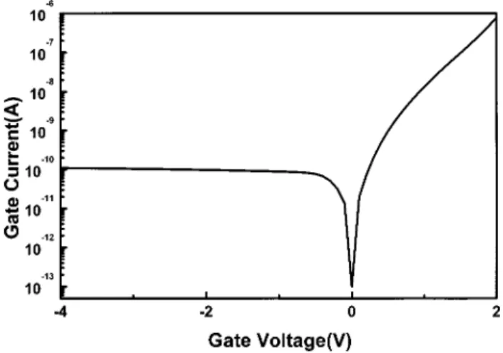
Figure 1 shows the typical current–voltage (I – V) curves of a PMOS diode with the oxide thickness of 2.7 nm. When the Al gate with the area of 3⫻10⫺4cm2 was under
positive bias, the electrons tunneled from the n-type silicon to the Al gate and the holes also tunneled from Al gate to
n-type silicon. As a result, a significant tunneling current was
observed in the positive gate bias. However, due to the dif-ferent barrier heights between electrons共⬃3.1 eV兲 and holes
共⬃5.6 eV兲, hole current may be smaller than the electron
current. Meanwhile, the positive gate bias also attracts elec-trons in the silicon/oxide interface to form an accumulation layer. The localized electrons in the accumulation layer have localized wave functions, which can have a spread in the reciprocal space and may provide extra momentum during the electron-hole radiative recombination. When the Al gate is under negative gate bias, the current is controlled by the thermal generated holes and is independent of negative gate bias.2
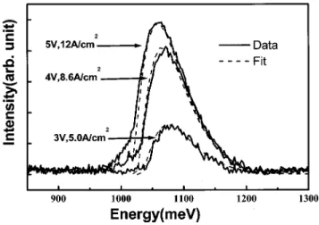
When significant current flowed through the PMOS structure under positive gate bias, luminescence was clearly observed under continuous wave operation without cooling. Since the light was blocked by the thick Al gate electrode, only the emission from the diode edge was detected, as ob-served by infrared viewer through a microscope. Figure 2 shows the emission spectra of an Al/2.7 nm oxide/n-silicon PMOS diode with a circular area of 4⫻10⫺2cm2. The emis-sion intensity increases with the positive gate bias. The peak width of our spectra increases from 68 to 86 meV, as the gate
a兲Electronic mail: [email protected]
b兲Also with: Institute of Electro-Optical Engineering. FIG. 1. The I–V curve of a PMOS diode. The EL is observed under positivegate bias.
APPLIED PHYSICS LETTERS VOLUME 76, NUMBER 12 20 MARCH 2000
1516
bias increase from 3 to 5 V. This width is about half of the previous data of the room-temperature spectra from the Si/ SiGe p-i-n diode.1The feature of the emission spectra is the asymmetrical broadening of the emission peak, where the high-energy part is broader than the low-energy part. This is very similar to the line shape of electron-hole-plasma recombination.4,5To confirm this observation, we fit the EL spectra by the line shape of EHP recombination using the following expression:
I共h兲⫽I0
冕
0h⫺Eg,EL
dEDe共E兲Dh共h⫺Eg,EL
⫺E兲f共E,Fe,T兲f 共h⫺Eg,EL⫺E,Fh,T兲, where De and Dh are the densities of states of electron and hole, respectively, Feand Fh are the respective quasi-Fermi energy, his the energy of photon emitted, T is the measure-ment temperature, Eg,ELis the band gap of Si obtained by the EL measurements, and the f’s are the Fermi-Dirac distribu-tion. In this expression, only the conservation of energy is taken into account. The momentum conservation required by the indirect bandgap nature of Si is assumed to be provided by the scattering of Si/oxide roughness8and/or the spread in the reciprocal space共k space兲 due to the localized wave func-tion of electrons in the accumulafunc-tion layer. The three-dimensional density of states关D(E)⬃E1/2兴 is used for holes, while a constant two-dimensional density of states is used for electrons in the accumulation layer. There are four adjustable parameters for the fitting: the relative intensity Io, the band gap Eg,EL, and the quasi-Fermi energy Feand Fh. The band gap determines the energy position of the spectra, and quasi-Fermi energies determine the line shapes of the spectra. A narrow peak is obtained, if the quasi-Fermi levels of elec-trons and holes lie closely in the band gap. A wide peak is obtained, if the quasi-Fermi levels of electrons and holes move deeply into the conduction band and the valence band, respectively. Figure 2 also shows the theoretical EHP spec-tra, indicating an excellent fit to the experimental data. The fitting parameters obtained in this work are quite different from those of the previous report.4,5 The quasi-Fermi ener-gies for both electrons and holes in our simulation lie within the band gap, while the quasi-Fermi energies of electrons and holes move into conduction band and valence band,
re-spectively, in the previous work.4,5 This indicates that the electron and hole concentrations in the tunneling PMOS di-odes are much smaller as compared to the Si/SiGe/Si quan-tum wells. As a result, the peak width in our work is much smaller, as compared to the previous reported data. The band gap obtained from the EHP model is about 1.01–1.03 eV for the gate voltage from 5 to 3 V, lower than the Si band gap of 1.12 eV at room temperature. This is unlikely to due to high junction temperature in Si/oxide interface, since the tempera-ture of 1.01 eV band gap is about 600 K and the EL spectra can not be fitted well using such high temperature. This re-duction of band gap can be understood by the surface band bending in the PMOS band diagram under the accumulation condition as shown in Fig. 3. The tunneling holes from the Al gate electrode injected into the valence band of n-Si will not stop at the interface, can probably reach the neutral re-gion of n-Si and relaxed to the valence band edge in the neutral region. The recombination of holes in the neutral region with the electrons in the accumulation region can emit photons with energy of the difference between the Si band gap and the surface band bending.
Besides the main emission peak 共NP兲, the relatively
FIG. 4. The dependence of peak intensity on current drive for a PMOS tunneling diode.
FIG. 2. The theoretical fitting of EL spectra from a PMOS tunneling diode.
FIG. 3. The schematic band diagram in the PMOS diode to explain the band gap reduction, obtained from the EHP model.
1517
week TO replica was also observed in PL spectra of the bulk of Si,4 relaxed SiGe,9 and strained SiGe.4,5 However, only one peak is observed in the EL spectra of the PMOS diode. The origin is not clear.
The dependence of the peak EL intensity on drive cur-rent is shown in Fig. 4. There is a superlinear increase of the output power with injection current. The efficiency seems to be enhanced at high current level. However, it is difficult to estimate the quantum efficiency, since the Al gate electrode blocks most light, and only the light emitted from the diode edge can be detected.
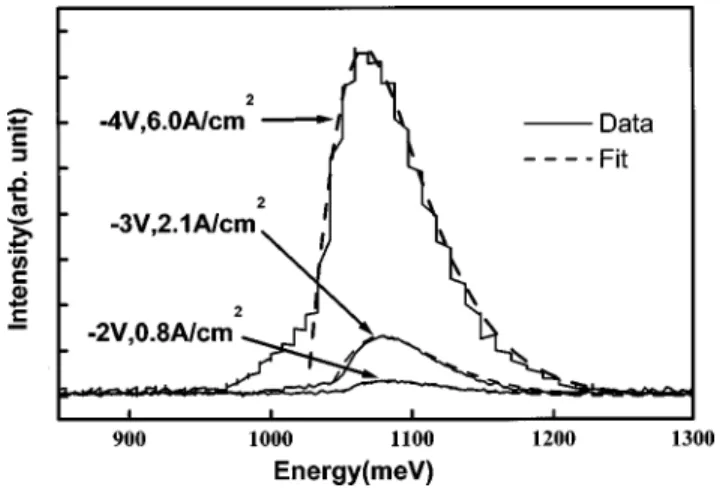
The EHP model also gives an excellent fit to EL spectra2,3 of the n-type MOS 共NMOS兲 tunneling diode as shown in Fig. 5. The band gap obtained from the fitting is
about 1.02–1.04 eV for the negative gate bias from 5 to 2.5 V, lower than the Si band gap. Similarly, the surface band bending is also responsible for this reduction
In summary, we presented the EL from the electron-hole plasma recombination in the MOS tunneling diodes. The EL spectra can be well fitted by a simple convolution of electron and hole distribution functions. The surface band bending in the Si/oxide interface is responsible for the reduced band gap, obtained from the EHP model. The relative narrow line width can be also understood by the fact that the positions of the quasi-Fermi energies of electrons and holes are both in the band gap.
This work is supported in part by National Science Council, Taiwan, Republic of China 共Nos. 88-2218-E-002-004 and 2112-M-002-038兲. The support of UMC and TSMC is also highly appreciated.
1Q. Mi, X. Xiao, J. C. Sturm, L. C. Lenchyshyn, and M. L. W. Thewalt,
Appl. Phys. Lett. 60, 3177共1992兲.
2
C. W. Liu, M. H. Lee, C. F. Lin, I. C. Lin, W. T. Liu, and H. H. Lin, Tech. Dig. Int. Electron Device Meet. 749共1999兲.
3C.-F. Lin, C. W. Liu, M.-J. Chen, M. H. Lee, and I. C. Lin, J. Phys.:
Condens. Matter共in press兲.
4X. Xiao, C. W. Liu, J. C. Sturm, L. C. Lenchyshyn, and M. L. Thewalt,
Appl. Phys. Lett. 60, 1720共1992兲.
5C. W. Liu, J. C. Sturm, Y. R. J. Lacroix, M. L. W. Thewalt, and D. D.
Perovic, Appl. Phys. Lett. 65, 76共1994兲.
6E. Cohen, M. D. Sturge, M. A. Olmstead, and R. A. Logan, Phys. Rev. B
22, 771共1980兲.
7
D. J. Robbins, P. Calcott, and W. Y. Leong, Appl. Phys. Lett. 59, 1350
共1991兲.
8M. Jaros and A. W. Beavis, Appl. Phys. Lett. 63, 669共1993兲. 9J. Weber and M. I. Alonso, Phys. Rev. B 40, 5683共1989兲. FIG. 5. The theoretical fitting of EL spectra from a NMOS tunneling diode.