Materials Chemistry and Physics 45 (1996) 92-96
Materials Science Communication
High performance non-alloyed pseudomorphic high electron
mobility transistors
C.K. Peng al*, W.H. Lana, S.L. Tua, S.J. Yang a, S.S. Chen b, CC. Lin b
a Materials R&D Center, Chung-Shari Institute of Science and Technology, P.O. Box 90005-S-6, Lung-ton, Tdwcm, ROC
b Institute of Materials Science cmd Engineering, National Chiao Tung Uniwsity, Hsinchrr, Tnhcnn, ROC
Received 19 December 1994; accepted 25 September 1995
Abstract
We have studied the InAs/GaAs strained layer superlattice (SLS) structures as non-alloyed contacts applied to pseudomorphic high electron mobility transistors (PHEMTs) grown by the molecular beam epitaxy (MBE) system. Transmission line measure-
ments with four point configurations showed that specific contact resistances between 6.6 x 10m7 and 2.6 x 10m6 Q cm2 were
obtained for the as-grown devices, with a linear correlation coefficient of 0.997. D.c. measurements of the as-grown PHEMT with 1 pm gate showed a transconductancc of 240 mS 111111-l. Microwave measurements on the same device showed a cut-off frequency of 19 GHz and a maximum power gain frequency of 42 GHz. These results are comparable with those of devices with the
conventional contact scheme. Meanwhile, since the non-alloying process maintains excellent surface morphology and sharp metal
pad edges, AuGeNi type metals can be used in small dimension devices. In contrast, the conventionally alloyed devices showed rough surface morphology and zigzag edges, which may affect device processing and limit the usefulness of AuGeNi metal as the
ohmic contact in small dimension devices.
Kqvwords: Strained layer superlattice; Non-alloyed contacts; Surface morphology
1. Introduction
Non-alloyed contact layers have attracted significant attention lately due to their superior properties in mak- ing low resistance ohmic contacts for III-V devices. Among them, InGaAs strained layers of various In compositions constitute an important category for such non-alloyed structures. It has been shown that contact resistances obtained for devices with non-alloyed con- tacts are comparable to, or even better than, those with conventional contacts. Meanwhile, because of the ex- emption of high temperature alloying processes, excel- lent device morphology may be maintained and simpler device processing and higher yield may be achieved,
While AuGe/Ni/Au has been used widely as a stan- dard n-type contact metal to III-V epitaxial layers due
* Corresponding author.
0254-0584/96/$15.00 0 1996 Elsevier Science S.A. All rights reserved
to the low eutectic point of AuGe alloy, the interaction of the alloy with the III-V layer underneath has led to ill defined edges which limit AuGeNi type metals for use in small dimension devices [ 11. However, adoption of the non-alloyed structure may be a cure for such limitations. In addition, since the alloying mechanism is not responsible for achieving low contact resistance in such a structure, refractory metals such as Pt/Ti [2] or Al [3] can be used as the contact metal, thus expanding the flexibility of the process design and making such a contact scheme of great value for better and more stable performance.
When using a non-alloyed structure, the material that the non-alloyed structure is grown onto plays an impor- tant role in determining the contact resistance. As a general rule, material of a lower energy band and with a smaller conduction band discontinuity at the hetero- junction makes a smaller energy barrier for electron transport among different layers, which leads to a better
C.K. Peng et al. /Matesials Chemistry and Physics 45 (1996) 92-96 93
n-type contact resistance and vice versa. Depending
upon whether the conduction channel is composed of
InGaAs, GaAs, or AlGaAs materials, non-alloyed spe-
cific contact resistances ranging between lo-* and
10m5 Q cm2 [4-61 have been obtained without anneal- ing. Different non-alloyed structures have been studied in III-V epilayers; the major scheme includes the pure InAs abrupt layer [4], the graded InGaAs layer [5], and the strained layer superlattice (SLS) composed of InAs, InGaAs, and GaAs layers, etc. [6], described in numer- ous publications. However, regardless of the extent of the study in using a non-alloyed structure for different device applications [7-g], there is very little published
data on using an InAs/GaAs SLS as a non-alloyed
structure on pseudomorphic high electron mobility
transistor (PHEMT) devices.
2. Experimental
In this paper, we describe our investigatation of
the application of the InAs/GaAs non-alloyed struc-
tures on PHEMT devices. The structure of the PHEMT consisted of an undoped 0.5 pm GaAs buffer, an un-
doped 1.50 A In o,lsGa,,,,As pseudomorphic layer, a
30 A Al,,,,Ga,,,,As undoped layer, a 500 A Si doped Al,,,,Ga,,,As layer of 2 x lOi* cmm3 doping concentra- tion, and a 150 A Si doped GaAs layer of 5 x 1Ol8 cmW3
concentration. Above the PHEMT, a non-alloyed con-
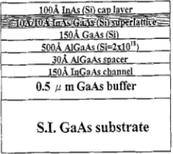
tact structure was grown which consisted of five periods of an InAs( 10 A) /GaAs( 10 I$) SLS and finally a 100 A InAs layer, all Si doped to 5 x 10¹⁸ cin3 concentration, as shown in Fig. 1.
The samples investigated in this study were grown on (100) GaAs epi-ready undoped substrate using a Riber
32P molecular beam epitaxy (MBE) system. For out-
gassing, the substrate temperature was slowly increased to 620 “C for a total of about 30 min to desorb the
surface oxide layer, before being brought down to
580 “C for the initiation of epitaxial growth. The entire device structure was grown at 580 “C under As-stabi- lized conditions, with the exception that the InGaAs channel layer was grown at 520 “C. The contact layers
laver
I
S.I. GaAs substrateFig. 1. Device structure for the non-alloyed PHEMT. On the top was a five period superlattice of InAsjGaAs (10 A/l0 A) followed by 100 8, of InAs layer as the non-alloyed contact structure.
were grown at between 450 and 500 “C due to the pres- ence of the In-containing layers. The reflection of high
energy electron diffraction (RHEED) showed clearly a
two by four pattern, signalizing readiness for growth. The transmission line contact structure was defined
using standard photolithography and conventional wet
chemical etching techniques. Mesa were formed using a
phosphoric-based chemical etching solution. Contact
patterns were then defined photolithographically, fol-
lowed by evaporation and lift-off of AuGe/Ni/Au
metals. As-grown samples; samples with 300 “C, 1 min annealing; samples with 460 “C, 1 min annealing; and the conventionally alloyed samples annealed at 460 “C for over 2 min were all prepared for comparison. Alloy- ing of the samples was performed in a tube furnace under flowing H2 for surface protection. Finally, the
InAs and the underlying layers between the contacts
were briefly etched to alleviate possible current conduc- tion through these highly doped contact layers. In device
processing, the same AuGe/Ni/Au metal system was
used as source and drain contact metal, while Al was used as gate metal.
3. Results and discussion
Contact resistances were measured using the well-
known extended transmission line model (ETLM). The
ETLM test pattern consists of square pads of
100 x 100 pm dimensions. Each set of patterns is com- posed of six different gap spacings varying from 3 to 17 pm. A four-point probe configuration was used for
resistance measurements to eliminate possible errors
introduced by the probe contact resistance. The specific contact resistance and sheet resistance were derived from a plot of the measured resistance versus gap spacing, using the least squares method to get a straight line fit to the experimental data. The ETLM plot is shown in Fig. 2, while the derived resistances are listed
in Table 1. For the as-grown sample, from the y
intercept and the slope, a contact resistance of 1.2 0 and a transfer resistance of 0.12 Qmm were obtained
corresponding to a specific contact resistance of
6.6 x lo-’ R cm2, with a linear correlation coefficient of 0.997. The slope of the straight line gave a sheet resis- tance of 220 Q/ 0, For the slightly and heavily annealed samples, specific contact resistances between 1 x 10m6 and 3 x lop6 R cm2 were obtained, while different batch processing had shown specific contact resistances in the high lo-’ R cm2 region. By carefully carrying out the
transmission line model (TLM) design and measure-
ment process, the possible error between the model and the measured data can be made insignificant [4].
The AuGe/Ni/Au alloy has been the most used metal
for making n-type ohmic contacts to III-V devices.
94 45 40 35 i 30 t 25 2 20 .Y 8 15 10 5 0
C.K. Peng et al. /Materials Chemistry and Physics 45 (1996) 92-96
0 5 10 15 20
Spacing (urn)
Fig. 2. Transmission line measurements of the device TLM pattern. Three different annealing conditions are shown, including (a) as- grown, (b) 300 “C, 1 min annealing, and (c) 460 “C, 1 min annealing. The inset shows the results after the conventional annealing treatment, where the decrease in the resistance for shorter spacing is evident.
Table 1
Transmission line measurements of the non-alloyed PHEMT samples Ml93 As-grown 300 ‘C, 1 min 460 ‘6, 1 min r, (0 cm2) 6.6 x IO-’ 1.09 x 10⁻⁶ 1.65 x 1O-6
Rs (d /lrn-‘) 2.17 2.14 2.14
440 “C or higher temperature needed for conventional
contacts increases the surface roughness and causes
lateral diffusion of the dopant atoms. It has been shown
that annealing at 440 “C for 2 min leads to edge deteri-
oration for a distance of up to 0.47 jtm [ 11, which may
limit the use of the AuGeNi metal in GaAs submicron
devices. For our test samples described earlier, we have
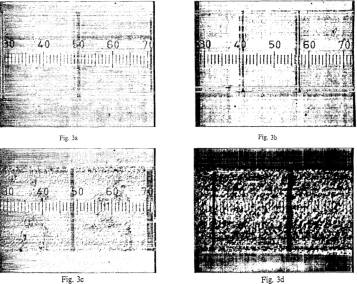
taken top view pictures by optical microscope, at 800 x
magnification, for comparison, as shown in Fig, 3. It is
obvious that for sample (b), annealed at 300 “C for
1 min, the metal surface is as good as the as-grown
samples (sample (a)), and the edges are straight and
sharply defined. The surface gets rougher for sample
(c), annealed at 460 “C for 1 min; however, the edges
Fig. 3a Fig. 3b
Fig. 3c
Fig. 3. Top view of differently treated samples using an optical microscope, at 800 x magnification. The surface gets rougher at 460 ‘C annealing
temperature, and then the edges become ill defined when the annealing lasts for longer than 2 min; (a) as-grown, (b) 300 ‘C, I min annealing, (c) 460 “C, 1 min annealing, and (d) 460 “C, > 2 min annealing.
C.K. Peng et al. /Materials Chemistry and Physics 45 (‘1996) 92-96 95
are still clearly defined. For the conventional annealing conditions of 460 “C for 2 min or longer, the surface becomes very rough and the edges zigzag. This latter phenomenon is consistent with the non-linearity of the TLM measurements, where the data for the 4 pm, and especially the 3 pm, spacing contact pads shows much smaller than expected resistance compared to a larger spacing contact pad, as shown in the inset of Fig. 2. On the other hand, the high linearity and low resistance TLM data of the as-grown and slightly annealed sam- ples indicate the usefulness of the non-alloyed scheme.
The uniform surface and well-defined edges of the
non-alloyed metal pads may relax the limit in using
AuGeNi type alloys for making low resistance ohmic
contacts for even small dimension submicron devices.
Van der Pauw Hall measurements on these non-
alloyed devices showed electron mobilities of 3200 and 15 680 cm2 V-’ s-l, and two-dimensional electron con- centrations (2-DEG) of 7.2 x 10” and 3.9 x 10¹² cmm2 at RT and 77 K, respectively. It should be noted that
these high 2-DEG data in non-alloyed devices are
partly contributed to by the non-alloyed layers. The d.c. drain current-voltage characteristics for the as-grown device with a 1 /Lrn gate length and a source-drain spacing of 3 pm are shown in Fig. 4. The I-V data show good pinch-off characteristics with a d.c. trans-
conductance of 240 mS mm-’ at a current level of
200 mA mm-‘, and a good breakdown voltage around
6 V. The source resistance is less than 0.1 R mm. The S-parameter of the devices was measured using a Cas-
cade microprobe station and a HP 851OC network
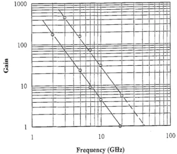
analyzer. Linear extrapolation of these data is shown in Fig. 5 with a current gain cut-off frequency (ft) around
19 GHz and a maximum oscillation frequency (fmaX) of
42 GHz. The bias voltages for this measurement were
V,, = -0.3 V and VDs = 2.0 V. These values are com-
ID CmA> 10.50 t I I 0 0 VDS .2500/div < v> 2. 0 Fig. 4. D.c. transconductance of the as-grown non-alloyed PHEMT with 1 pm gate length. The best gain was around 240 mS mm-‘, gate biased between 0.4 V and - 1.0 V at 0.2 V per step.
1000 100 .9 5 10 1 1 10 Frequency (GHz)
Fig. 5. Microwave current gain cut-off frequency (/J and power gain frequency (f,,,) characteristics for the non-alloyed 1 pm PHEMT.
parable with our other alloyed PHEMT devices of
similar configuration but with a conventional GaAs(Si) cap layer instead of the non-alloyed contact layers.
4. Conclusions
In conclusion, we have shown that the InAs/GaAs
SLS can be used as an excellent non-alloyed ohmic
contact for PHEMT devices. Specific contact resis-
tances as low as 6.6 x 10v7 Q cm2 were obtained, which are comparable to a good conventional contact with a
high temperature annealing. Low contact resistances
and well defined edges of the non-alloyed contact pads indicate that the limit of using AuGeNi metal in small dimension devices, due to interface interaction during alloying, can be lifted. The d.c. transconductance of the
non-alloyed PHEMT was 240 mS mm-l. The current
gain and the power gain cut-off frequencies were 19 and 42 GHz, respectively, for the 1 pm gate device.
Acknowledgements
The authors would like to thank C.J. Chang and
K.F. Peng for their invaluable assistance in device
fabrication and MBE growth.
References
[l] Y.C. Shih, M. Murakami, E.L. Wilkie and A.C. Callegari, J. Appl. Phys., 62 (1987) 582.
[2] A. Katz, CR. Abernathy and S.J. Pearton, Appl. Phys. Lett., 56 (1990) 1208.
[3] M. Missous, E.H. Rhoderick and K.E. Singer, J. Appl. Phys., 59 (1986) 3189.
96 C.K. Peng et al. /Materials Chemistry and Physics 45 (1996) 92-96 [4] C.K. Peng, J. Chen, J. Chyi and H. Morkoc, J. Appl. Phys., 64
(1988) 429.
[5] S. Kuroda, N. Harada, T. Katakami, T. Mimura and M. Abe, IEEE Trans. Electron Devices, 36 (1989) 2196.
[6] C.K. Peng, G. Ji, N.S. Kumar and H. Morkoc, Appl. Phys. Lett., 53 (1988) 900.
[7] N.S. Kumar, J.I. Chyi, C.K. Peng and I-1. Morkoc, Appl. Phys. Lett., 55 (1989) 570.
[S] J.H. Huang, J.K. Abrokwah and W.J. Ooms, Appl. Phyz. Left,, 61 (1992) 2455.
[9] F. Ren, CR. Abernathy, S.J. Pearton and P.W. Wisk, Appl. Phys. Lett., 64 (1994) 1508.