Improvement in output power of a 460 nm InGaN light-emitting diode using staggered
quantum well
Chih-Teng Liao, Miao-Chan Tsai, Bo-Ting Liou, Sheng-Horng Yen, and Yen-Kuang Kuo
Citation: Journal of Applied Physics 108, 063107 (2010); doi: 10.1063/1.3471804
View online: http://dx.doi.org/10.1063/1.3471804
View Table of Contents: http://scitation.aip.org/content/aip/journal/jap/108/6?ver=pdfcov Published by the AIP Publishing
Articles you may be interested in
Improvement in spontaneous emission rates for InGaN quantum wells on ternary InGaN substrate for light-emitting diodes
J. Appl. Phys. 110, 113110 (2011); 10.1063/1.3668117
Growths of staggered InGaN quantum wells light-emitting diodes emitting at 520–525 nm employing graded growth-temperature profile
Appl. Phys. Lett. 95, 061104 (2009); 10.1063/1.3204446
High-efficiency staggered 530 nm InGaN/InGaN/GaN quantum-well light-emitting diodes Appl. Phys. Lett. 94, 041109 (2009); 10.1063/1.3075853
Polarization engineering via staggered InGaN quantum wells for radiative efficiency enhancement of light emitting diodes
Appl. Phys. Lett. 91, 091110 (2007); 10.1063/1.2775334
Carrier leakage in InGaN quantum well light-emitting diodes emitting at 480 nm Appl. Phys. Lett. 82, 2755 (2003); 10.1063/1.1570515
Improvement in output power of a 460 nm InGaN light-emitting diode using
staggered quantum well
Chih-Teng Liao,1 Miao-Chan Tsai,2 Bo-Ting Liou,3 Sheng-Horng Yen,4 and Yen-Kuang Kuo5,a兲
1
Institute of Lighting and Energy Photonics, College of Photonics, National Chiao Tung University, Tainan 711, Taiwan
2Institute of Photonics, National Changhua University of Education, Changhua 500, Taiwan 3Department of Mechanical Engineering, Hsiuping Institute of Technology, Taichung 41283, Taiwan 4R&D division, Epistar Co., Ltd., Science-based Industrial Park, Hsinchu 300, Taiwan
5Department of Physics, National Changhua University of Education, Changhua 500, Taiwan 共Received 18 June 2010; accepted 6 July 2010; published online 24 September 2010兲
Staggered quantum well structures are studied to eliminate the influence of polarization-induced electrostatic field upon the optical performance of blue InGaN light-emitting diodes共LEDs兲. Blue InGaN LEDs with various staggered quantum wells which vary in their indium compositions and quantum well width are theoretically studied and compared by using theAPSYSsimulation program. According to the simulation results, the best optical characteristic is obtained when the staggered quantum well is designed as In0.20Ga0.80N 共1.4 nm兲–In0.26Ga0.74N 共1.6 nm兲 for blue LEDs. Superiority of this novelty design is on the strength of its enhanced overlap of electron and hole wave functions, uniform distribution of holes, and suppressed electron leakage in the LED device. © 2010 American Institute of Physics.关doi:10.1063/1.3471804兴
I. INTRODUCTION
The visible III-nitride light-emitting diodes共LEDs兲 have received much attention due to their wide applications in full-color display, liquid crystal display back-lighting, mobile platforms, and illumination.1–6High-luminescence and high-efficiency blue InGaN LEDs, especially, are of foremost im-portance for application in illumination market such as out-door display and solid-state lighting. However, several mechanisms degenerating the optical performance including light extraction efficiency, current crowding effect, high op-eration voltage, and piezoelectric effect remain unsolved which will sabotage the achievement of high-power blue In-GaN LEDs.7–11
For the III-nitride system, the electrostatic field within the active region is a critical factor to poor lighting charac-teristic. Resulting from spontaneous and piezoelectric polar-izations, the piezoelectric effect eventually leads to strong electrostatic field and band bending situation within the ac-tive region. Piezoelectric polarization is caused by stress formed in the situation when layers were grown on a lattice-mismatch substrate; spontaneous polarization results from the asymmetric structure along the 关0001兴 axis of wurtzite structures.12–14The large electrostatic field within the active region results in quantum confined Stark effect and poor overlap of electron and hole wave functions, and it conse-quently reduces the radiative recombination rate and internal quantum efficiency of the optoelectronic devices. To mini-mize the piezoelectric effect of blue InGaN LEDs, several specific structure designs such as heavily Si-doping in quan-tum barriers,15–17 nonpolar共a- and m-planes兲 quantum wells 共QWs兲 grown on r-plane sapphire and␥-LiAlO2,18–22
semi-polar QWs grown on m-plane sapphire,23–27 polarization-matched AlGaInN layers,28,29 and staggered-QW structures have been proposed.30–39For InGaN LEDs, as the overlap of electron and hole wave functions improves, the photolumi-nescence lifetime will decrease, and the radiative recombina-tion rate and optical gain will be accordingly enhanced; hence, the percentage of carrier leakage would be reduced owing to carriers that effectively contribute toward radiative recombination. In addition, although the above-mentioned methods are useful for abating the piezoelectric effect, staggered-InGaN QW LEDs have the merit of an identical growth process to the conventional structures that makes commercial fabrication possible and substantial. After the concept of the staggered-InGaN-QW structure was proposed by Arif et al.30 for the first time, various similar designs including type-II InGaN QW,40–42 strain-compensated InGaN-AlGaN QW,43,44 three-layer staggered-InGaN QW,35,36,39 InGaN QW with AlGaN ␦-layer,45–47 and dip-shaped InGaN/GaN QW 共Ref.37兲 have been recommended
to decrease the strong polarization-induced electrostatic field in the GaN-based optoelectronic devices. Therefore, the fo-cus of the current research is upon staggered-QW LEDs; by adjusting the indium composition and well width of the stag-gered QWs, the authors seek to accomplish better optical performance of blue InGaN LEDs.
In this work, various staggered-InGaN QW LEDs are theoretically studied in detail by using the APSYS
共abbrevia-tion of advanced physical models of semiconductor devices兲48
simulation program. By performing computational simulations, the authors examine proper designs of staggered-QW blue LEDs and the critical physical mecha-nisms behind the improvement of the optical performance. a兲Electronic mail: [email protected].
共2010兲
0021-8979/2010/108共6兲/063107/6/$30.00 108, 063107-1 © 2010 American Institute of Physics
II. SIMULATION PARAMETERS AND DEVICE STRUCTURE
The band gap energies of GaN, AlN, InN, and other binary alloys at temperature T can be expressed by the Varshni formula49
Eg共T兲 = Eg共0兲 −
␣· T2
T +, 共1兲
where Eg共T兲 is the band gap energy at temperature T, Eg共0兲
is the band gap energy at 0 K,␣ and are material-related constants. TableI lists the band gap energies of GaN, AlN, and InN used in our simlulation.49,50Besides, for InxGa1−xN and AlxGa1−xN ternary alloys, the band gap energies can be described as a linear combination of GaN, AlN, or InN bi-nary alloys and a second-order correction as the following formula:51
Eg共InxGa1−xN兲 = Eg,InN· x + Eg,GaN·共1 − x兲 − b · x · 共1
− x兲, 共2兲
Eg共AlxGa1−xN兲 = Eg,AlN· x + Eg,GaN·共1 − x兲 − b · x · 共1
− x兲, 共3兲
where Eg共InxGa1−xN兲 and Eg共AlxGa1−xN兲 are the band gap energies of InxGa1−xN and AlxGa1−xN, and the band gap bowing parameters, b, of InxGa1−xN and AlxGa1−xN are adopted to be 2.8 eV and 0.7 eV, respectively.52 Other mate-rial parameters of the relevant binary semiconductors used in the simulation can be found in Ref.52.
In addition, it is important to take into consideration the built-in polarization induced by spontaneous and piezoelec-tric polarizations at heterointerfaces of nitride related devices since it plays an essential role for III-nitride optical devices. To calculate the built-in polarization induced by spontaneous and piezoelectric polarizations at heterointerfaces of III-nitride LEDs, the method developed by Bernardini12 is em-ployed to estimate the fixed interface charges. The spontane-ous polarization of ternary nitride alloys can be expressed by the formulas with bowing terms as shown in Eqs.共4兲and共5兲
Psp共AlxGa1−xN兲 = x · Psp共AlN兲 + 共1 − x兲 · Psp共GaN兲 + B共AlGaN兲 · x · 共1 − x兲, 共4兲 Psp共InxGa1−xN兲 = x · Psp共InN兲 + 共1 − x兲 · Psp共GaN兲
+ B共InGaN兲 · x · 共1 − x兲, 共5兲 where Psp共InN兲, Psp共AlN兲, and Psp共GaN兲 are values of spon-taneous polarization of InN, AlN, and GaN alloys, which are set to be −0.042 C/m2, −0.090 C/m2, and −0.034 C/m2,
respectively; B共InGaN兲 and B共AlGaN兲 are spontaneous po-larization bowing parameters of InGaN and AlGaN, which are −0.037 C/m2and −0.021 C/m2, respectively.52
On the other hand, the piezoelectric polarization of Al-GaN and InAl-GaN can be calculated by the following formu-las:
Ppz共AlxGa1−xN兲 = Ppz共AlN兲 · x + Ppz共GaN兲 · 共1 − x兲, 共6兲
Ppz共InxGa1−xN兲 = Ppz共InN兲 · x + Ppz共GaN兲 · 共1 − x兲, 共7兲 where
Ppz共AlN兲 = − 1.808 · + 5.624 · 2 for ⬍ 0, 共8兲 Ppz共AlN兲 = − 1.808 · − 7.888 · 2 for ⬎ 0, 共9兲
Ppz共GaN兲 = − 0.918 · + 9.541 · 2, 共10兲
Ppz共InN兲 = − 1.373 · + 7.559 · 2. 共11兲 The basal strain matched to a GaN layer for the alloy in this study is defined as
= 共asub− a兲/a, 共12兲
where asuband a are the lattice constants of GaN and alloy layers, respectively. Total polarization is obtained by sum-ming the values of spontaneous and piezoelectric polariza-tions. Note that the amount of surface charges obtained from the experimental measurement is usually smaller than those obtained by theoretical calculation. The surface charges could be screened due to the defects inside the device and the screening percentage commonly ranges between 20% and 80% for InGaN materials.53,54 To ascertain identical results of the simulated data to the original structure, approach real situation, 40% of the calculated surface charge density is assumed in our simulation.
The simulated InGaN blue LED used as a reference for subsequent analysis is based on the structure fabricated by Chang et al.55The device geometry was a rectangular shape design with dimensions of 400⫻320 m2. This LED was grown on a c-plane sapphire substrate, followed by a GaN buffer layer. A 3 m thick Si-doped n-GaN layer with a doping concentration of 1⫻1018 cm−3 was used to be the n-type contact layer. The active region consisted of five 3 nm thick In0.23Ga0.77N QWs separated by six 7 nm thick GaN barriers. On top of the active region was a 50 nm thick Mg-doped p-Al0.15Ga0.85N electron-blocking layer共EBL兲 with a doping concentration of 3⫻1017 cm−3. A 0.25 m thick Mg-doped p-GaN contact layer with a doping concentration of 5⫻1017 cm−3 was grown to complete the structure.
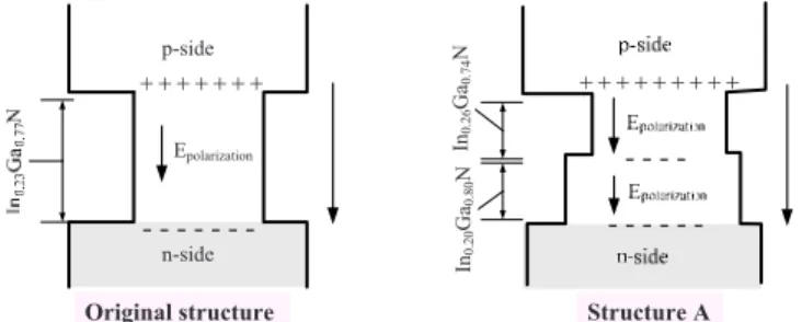
To simplify the structure referred, the number of QW in our simulation is remained to be one. Therefore, the subse-quent investigations are for the blue InGaN LED with single QW共SQW兲 and the schematic diagram could be referred in Fig. 1. To model the staggered-QW structure, the original In0.23Ga0.77N QW layer is divided into two layers, which are layer I close to the n-layers and layer II close to the p-layers; the schematic diagram of the staggered-QW is presented in Fig.2. Note that the total thickness of the InGaN QW is fixed for all the structures considered in the subsequent discussion.
TABLE I. Band gap energy of GaN, AlN, and InN.
Parameter
Alloy
GaN AlN InN
Eg共0兲 共eV兲 3.507 6.23 0.735
␣共meV/K兲 0.909 1.799 0.245
共K兲 830 1462 624
063107-2 Liao et al. J. Appl. Phys. 108, 063107共2010兲
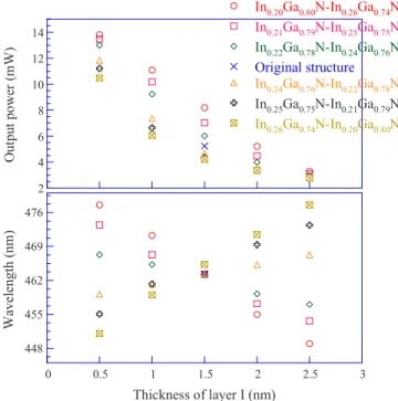
Steps in exploring the most appropriate design of layers I and II in the simulation are illustrated as the following. First, the indium composition of layer I increased from 0.20 to 0.26 while that of layer II decreased from 0.26 to 0.20, cor-respondingly. Then, the width of layer I changed from 0.5 to 2.5 nm and that of layer II changed from 2.5 nm to 0.5 nm accordingly. Figure3 shows the output power and emission wavelength of each staggered-QW LED of which the indium composition for each structure ranges from 0.20 to 0.26 and well width ranges from 0.5 to 2.5 nm. Based on Fig.3, the authors enumerated a few appropriate staggered-QW designs which sustained the InGaN LEDs emitting at approximately 460 nm and, at the same time, enhanced the lighting power of the devices. After comparing, preferable designs of the staggered QWs are In0.20Ga0.80N共1.4 nm兲–In0.26Ga0.74N共1.6 nm兲, In0.21Ga0.79N 共1.4 nm兲–In0.25Ga0.75N 共1.6 nm兲, and In0.22Ga0.78N 共1.5 nm兲–In0.24Ga0.76N 共1.5 nm兲, which are named as structure A, structure B, and structure C, respec-tively.
III. SIMULATION RESULTS AND DISCUSSION
The simulated light-current-voltage共L-I-V兲 performance curves of structure A, B, and C, as well as the original one are plotted in Fig.4. From Fig. 4, it is apparent that all the three staggered-QW LEDs possess better lighting character-istic than the original one while the electrical performances of these devices are similar. To scrutinize the main physical factors to the improvement in the lighting performance of staggered-QW LEDs, optical characteristics of structure A possessing the best performance and the original structure, including band diagram, overlap between electron and hole
wave functions in the QW, electrostatic field, and carrier dis-tribution, are compared and discussed in the following para-graph.
First, the emission spectra of structure A and the original structure are plotted in Fig. 5. The emitting spectra are peaked at around 460 nm and furthermore the spontaneous emission rate of structure A is effectively enhanced as com-pared with the original structure. In Fig.6, the band diagrams with ground-state electron and hole wave functions of struc-ture A and the original strucstruc-ture at 20 mA are presented. It could be found that for structure A which features a design of InGaN QW, the tilted valence band within the QW is re-formed because of the step-like shape. In another word, structure A has the merit of more uniform distribution of holes inside the QW when compared with the original struc-ture. As a result of right-shifted hole wave function, the over-lap of electron and hole wave functions in structure A is improved. The percentage of overlap between electron and hole wave functions is 14.9% for structure A and 13.9% for the original structure.
Second, the electron concentration and conduction band
FIG. 1. 共Color online兲 Schematic diagram of the SQW LED in this study.
FIG. 2.共Color online兲 Schematic diagram of the staggered-QW.
2 4 6 8 10 12 14 In0.20Ga0.80N-In0.26Ga0.74N In0.21Ga0.79N-In0.25Ga0.75N In0.22Ga0.78N-In0.24Ga0.76N Original structure In0.24Ga0.76N-In0.22Ga0.78N In0.25Ga0.75N-In0.21Ga0.79N In0.26Ga0.74N-In0.20Ga0.80N O ut pu tpowe r (m W) 448 455 462 469 476 0 0.5 1 1.5 2 2.5 3 Thickness of layer I (nm) Wave lengt h( nm )
FIG. 3. 共Color online兲 Output power and emission wavelength of varied staggered-QW LEDs. 0 5 10 15 20 25 0 1 2 3 4 5 6 7 8 0 10 20 30 40 50 Structure A Structure B Structure C Original structure Ou tp ut po we r (mW ) Current (mA) Vo lta ge( V )
FIG. 4. 共Color online兲 Simulated L-I-V curves of structure A, B, C, and original structure.
in the active region for structure A and the original structure at 20 mA are shown in Fig.7共a兲while the hole concentration and valence band for them are presented in Fig. 7共b兲. The gray areas in the figures represent the locations of the QW. For ordinary blue InGaN LEDs, since holes are the minority carriers in the active region, the radiative emission is domi-nated mainly by holes. It can be easily observed that hole distribution within the QW for structure A is right-shifted due to little sagged valence band as shown in Fig. 7共b兲. Moreover, the negative electrostatic field within the active region of structure A is larger than that of the original struc-ture as indicated in Fig. 8. Figure 9 schematically presents the polarization charges at each interface within the active region for structure A and the original structure. The strengthened negative electrostatic field of structure A results from the larger lattice-mismatch between the In0.26Ga0.74N well layer and the GaN barrier layer as compared with the difference between the In0.23Ga0.77N well layer and the GaN barrier layer in the original structure as shown in Fig. 9. Since a large negative electrostatic field contributes to hole injection into the QW, consequently, it is anticipated that,
compared with the original structure, structure A may pos-sess more holes inside the QW. When comparing the area under the curves of hole concentration for these two struc-tures, we conclude an increase of 1% of the hole concentra-tion inside the QW in structure A. Given that right-shifted hole distribution and larger amounts of holes inside the QW lead to improvement in overlap of electrons and holes, the recombination of electrons and holes is enhanced, and the emission power is increased correspondingly in structure A. Third, Fig.10indicates the conduction band diagrams of structure A and the original structure at 20 mA. After calcu-lating, the effective potential heights of structure A and the original structure共which are the difference between the con-duction band energy of the EBL and quasi-Fermi level兲 are 201 meV and 173 meV, respectively. Due to larger effective potential height, structure A has a smaller percentage of elec-tron leakage of 6.5% when compared with the original struc-ture共11.9%兲. In other words, larger amounts of holes inside the QW as well as increased overlap of electron and hole 0 1 2 3 4 5 6 7 400 420 440 460 480 500 Structure A Original structure @ 20 mA Wavelength (nm) Spon ta neous em is si on ra te (a.u. )
FIG. 5.共Color online兲 Emission spectra of structure A and original structure at 20 mA. 0 1 2 3 4 83.000 83.005 83.010 83.015 83.020 Ener gy (eV ) Distance (μm) quasi-Fermi level n-side @ 20 mA Structure A Γe-h= 14.9% (a) 0 1 2 3 4 83.000 83.005 83.010 83.015 83.020 Energy (e V ) Distance (μm) quasi-Fermi level n-side @ 20 mA Original structure Γe-h= 13.9% (b)
FIG. 6. 共Color online兲 Band diagrams with ground-state electron and hole wave functions of共a兲 structure A and 共b兲 original structure at 20 mA.
0 14 28 42 2 2.5 3 3.5 83.000 83.005 83.010 83.015 83.020 Structure A Original structure Distance (μm) Ene rgy (e V ) @ 20 mA (a)E lect ron co ncent ra tion (10 18 /c m 3 ) 0 1 2 3 4 5 6 7 8 -0.6 -0.4 -0.2 0 0.2 0.4 83.000 83.005 83.010 83.015 83.020 Structure A Original structure H ole concen tr at io n (10 18 /c m 3 ) E nergy (e V) Distance (μm) (b) @ 20 mA
FIG. 7. 共Color online兲 共a兲 Electron concentration together with conduction band diagram and共b兲 hole concentration together with valence band dia-gram for structure A and original structure at 20 mA.
-20 -15 -10 -5 0 5 83.004 83.008 83.012 83.016 83.020 Structure A Original structure Distance (μm) E lect ros ta ti c fi el d (10 5 V/ cm ) @ 20 mA n-side
FIG. 8.共Color online兲 Built-in electrostatic field within the active region of structure A and original structure at 20 mA.
063107-4 Liao et al. J. Appl. Phys. 108, 063107共2010兲
wave functions result in more electrons contributing to radia-tive recombination. Therefore, the issue of electron leakage, accordingly, is diminished.
Finally, considering the Shockley–Read–Hall共SRH兲 re-combination rate of structure A and the original structure at 20 mA共see Fig. 11兲, the authors integrated areas under the
curves of SRH recombination rates for the two structures and found that structure A possessed less SRH recombination, which is the effect of nonradiative recombination. Therefore, for structure A, owing to an increase in overlap of electron and hole wave functions, there will be less carriers inside the QW recombining via nonradiative recombination process and more carriers through radiative recombination process when compared with the original structure.
IV. CONCLUSION
Optical characteristics of various staggered-InGaN-QW LEDs, which are designed to debase the significant piezo-electric effect of blue InGaN LEDs, are numerically investi-gated in this study by using theAPSYS simulation program. Indium composition and width of the staggered-QW are ad-justed to obtain the optimal structure and the corresponding optical performance including emission wavelength, band diagram, and carrier distribution are investigated and com-pared. According to the simulation results, predicaments such as overlap of electron and hole wave functions, inho-mogeneous carrier distribution inside the QW, electron leak-age, and SRH recombination rate in the active region are remarkably improved in the In0.20Ga0.80N 共1.4 nm兲–In0.26Ga0.74N 共1.6 nm兲 staggered-QW structure. There-fore, it is concluded that the best optical performance is ob-tained in the blue InGaN LED characterized by the design of an In0.20Ga0.80N共1.4 nm兲–In0.26Ga0.74N共1.6 nm兲 QW.
ACKNOWLEDGMENTS
This work is supported by the National Science Council 共NSC兲 of Taiwan under Grant No. NSC 96-2112-M-018-007-MY3. The authors are grateful to Crosslight Software Inc., Canada, for the development of the APSYS simulation pro-gram used in this study and Dr. Jen-De Chen for the techni-cal assistance.
1J. Shakya, K. Knabe, K. H. Kim, J. Li, J. Y. Lin, and H. X. Jiang,Appl.
Phys. Lett.86, 091107共2005兲.
2J. Li, J. Y. Lin, and H. X. Jiang,Appl. Phys. Lett.88, 171909共2006兲. 3Y. A. Chang, C. Y. Luo, H. C. Kuo, Y. K. Kuo, C. F. Lin, and S. C. Wang,
Jpn. J. Appl. Phys., Part 144, 7916共2005兲.
4P. T. Barletta, E. A. Berkman, B. F. Moody, N. A. El-Masry, A. M. Emara,
M. J. Reed, and S. M. Bedair,Appl. Phys. Lett.90, 151109共2007兲. 5K. S. Kim, J. H. Kim, S. J. Jung, Y. J. Park, and S. N. Cho,Appl. Phys.
Lett.96, 091104共2010兲.
6S. Choi, H. J. Kim, S.-S. Kim, J. Liu, J. Kim, J.-H. Ryou, R. D. Dupuis, A.
M. Fischer, and F. A. Ponce,Appl. Phys. Lett.96, 221105共2010兲. 7C. H. Kuo, S. J. Chang, Y. K. Su, L. W. Wu, J. F. Chen, J. K. Sheu, and J.
M. Tsai, IEEE Trans. Electron Devices 50, 535共2003兲.
8Y. K. Su, S. J. Chang, S. C. Wei, R. W. Chuang, S. M. Chen, and W. L. Li,
IEEE Electron Device Lett.26, 891共2005兲.
9C. F. Shen, S. J. Chang, W. S. Chen, T. K. Ko, C. T. Kuo, and S. C. Shei,
IEEE Photonics Technol. Lett.19, 780共2007兲.
10T. Onuma, H. Amaike, M. Kubota, K. Okamoto, H. Ohta, J. Ichihara, H.
Takasu, and S. F. Chichibu,Appl. Phys. Lett.91, 181903共2007兲. 11C. E. Lee, H. C. Kuo, Y. C. Lee, M. R. Tsai, T. C. Lu, S. C. Wang, and C.
T. Kuo,IEEE Photonics Technol. Lett.20, 184共2008兲.
12F. Bernardini, in Nitride Semiconductor Devices: Principles and Simula-tion, edited by J. Piprek共Wiley, New York, 2007兲, p. 4968.
13A. Thamm, O. Brandt, J. Ringling, A. Trampert, and K. H. Ploog,Phys.
Rev. B61, 16025共2000兲.
14A. E. Romanov, T. J. Baker, S. Nakamura, and J. S. Speck,J. Appl. Phys. 100, 023522共2006兲.
15Y.-H. Cho, J. J. Song, S. Keller, M. S. Minsky, E. Hu, U. K. Mishra, and
S. P. DenBaars,Appl. Phys. Lett.73, 1128共1998兲.
16E. Oh, C. Sone, O. Nam, H. Park, and Y. Park,Appl. Phys. Lett.76, 3242
共2000兲.
17G. Franssen, T. Suski, P. Perlin, R. Bohdan, A. Bercha, W. Trzeciakowski,
I. Makarowa, P. Prystawko, M. Leszczyński, I. Grzegory, S. Porowski, and S. Kokenyesi,Appl. Phys. Lett.87, 041109共2005兲.
18P. Waltereit, O. Brandt, A. Trampert, H. T. Grahn, J. Menniger, M.
Ram-steiner, M. Reiche, and K. H. Ploog,Nature共London兲406, 865共2000兲. 19A. Chakraborty, B. A. Haskell, S. Keller, J. S. Speck, S. P. DenBaars, S.
Nakamura, and U. K. Mishra,Appl. Phys. Lett.85, 5143共2004兲. 20R. Kröger, T. Paskova, S. Figge, D. Hommel, A. Rosenauer, and B.
Mon-emar,Appl. Phys. Lett.90, 081918共2007兲.
21A. Kobayashi, S. Kawano, K. Ueno, J. Ohta, H. Fujioka, H. Amanai, S.
Nagao, and H. Horie,Appl. Phys. Lett.91, 191905共2007兲. 22T. Paskova,Phys. Status Solidi245, 1011共2008兲 共b兲.
23A. Chakraborty, T. J. Baker, B. A. Haskell, F. Wu, J. S. Speck, S. P.
DenBaars, S. Nakamura, and U. K. Mishra,Jpn. J. Appl. Phys., Part 144,
L945共2005兲.
24R. Sharma, P. M. Pattison, H. Masui, R. M. Farrell, T. J. Baker, B. A. p-side n-side + + + + + + + -Epolarization Original structure + + + + + + + + + -In0.20 Ga 0.80 N In0.26 Ga 0.74 N Structure A
FIG. 9. 共Color online兲 Schematic diagram of polarization charges at each interface within the active region for structure A and original structure.
2.8 3 3.2 3.4 3.6 83.000 83.005 83.010 83.015 83.020 Structure A Original structure quasi-Fermi level @ 20 mA n-side Ener gy (eV ) Distance (μm)
Effective potential height
FIG. 10.共Color online兲 Conduction band diagrams of structure A and origi-nal structure at 20 mA.
0 0.05 0.1 0.15 0.2 83.000 83.005 83.010 83.015 83.020 Structure A Original structure S R H recombi nat ion rat e (10 28 cm − 3/s ) Distance (μm) n-side @ 20 mA
FIG. 11. 共Color online兲 SRH recombination rate of structure A and original structure at 20 mA.
Haskell, F. Wu, S. P. DenBaars, J. S. Speck, and S. Nakamura,Appl. Phys.
Lett.87, 231110共2005兲.
25M. Ueda, K. Kojima, M. Funato, Y. Kawakami, Y. Narukawa, and T.
Mukai,Appl. Phys. Lett.89, 211907共2006兲.
26K. Kojima, M. Funato, Y. Kawakami, S. Masui, S. Nagahama, and T.
Mukai,Appl. Phys. Lett.91, 251107共2007兲.
27P. Vennéguès, Z. Bougrioua, and T. Gunehne,Jpn. J. Appl. Phys., Part 1 46, 4089共2007兲.
28M.-H. Kim, M. F. Schubert, Q. Dai, J. K. Kim, E. F. Schubert, J. Piprek,
and Y. Park,Appl. Phys. Lett.91, 183507共2007兲.
29M. F. Schubert, J. Xu, J. K. Kim, E. F. Schubert, M. H. Kim, S. Yoon, S.
M. Lee, C. Sone, T. Sakong, and Y. Park,Appl. Phys. Lett.93, 041102
共2008兲.
30R. A. Arif, Y.-K. Ee, and N. Tansu,Appl. Phys. Lett.91, 091110共2007兲. 31R. A. Arif, H. Zhao, Y.-K. Ee, and N. Tansu,IEEE J. Quantum Electron.
44, 573共2008兲.
32S.-H. Yen and Y.-K. Kuo,Opt. Commun.281, 4735共2008兲.
33S.-H. Park, D. Ahn, B.-H. Koo, and J.-W. Kim,Phys. Status Solidi A206,
2637共2009兲.
34H. Zhao, R. A. Arif, and N. Tansu,IEEE J. Sel. Top. Quantum Electron. 15, 1104共2009兲.
35H. Zhao, G. Liu, X.-H. Li, G. S. Huang, J. D. Poplawsky, S. T. Penn, V.
Dierolf, and N. Tansu,Appl. Phys. Lett.95, 061104共2009兲.
36H. P. Zhao, G. Y. Liu, X. H. Li, R. A. Arif, G. S. Huang, J. D. Poplawsky,
S. T. Penn, V. Dierolf, and N. Tansu,IET Optoelectron.3, 283共2009兲. 37S.-H. Park, D. Ahn, B.-H. Koo, and J.-W. Kim,Appl. Phys. Lett.95,
063507共2009兲.
38S.-H. Park, D. Ahn, and J.-W. Kim,Appl. Phys. Lett.94, 041109共2009兲. 39H. Zhao and N. Tansu,J. Appl. Phys.107, 113110共2010兲.
40R. A. Arif, H. Zhao, and N. Tansu,Appl. Phys. Lett.92, 011104共2008兲. 41H. Zhao, R. A. Arif, and N. Tansu,J. Appl. Phys.104, 043104共2008兲. 42S.-H. Park, D. Ahn, B.-H. Koo, and J.-E. Oh,Appl. Phys. Lett.96, 051106
共2010兲.
43H. Zhao, R. A. Arif, Y.-K. Ee, and N. Tansu,Opt. Quantum Electron.40,
301共2008兲.
44H. Zhao, R. A. Arif, Y.-K. Ee, and N. Tansu,IEEE J. Quantum Electron. 45, 66共2009兲.
45J. Park and Y. Kawakami,Appl. Phys. Lett.88, 202107共2006兲. 46J. Park, A. Kaneta, M. Funato, and Y. Kawakami,IEEE J. Quantum
Elec-tron.42, 1023共2006兲.
47S.-H. Park, J. Park, and E. Yoon,Appl. Phys. Lett.90, 023508共2007兲. 48
APSYS by Crosslight Software Inc., Burnaby, Canada, http:// www.crosslight.com
49I. Vurgaftman, J. R. Meyer, and L. R. Ram-Mohan, J. Appl. Phys.89,
5815共2001兲.
50T. Matsuoka, H. Okamoto, M. Nakao, H. Harima, and E. Kurimoto,Appl.
Phys. Lett.81, 1246共2002兲.
51G. B. Stringfellow and M. G. Craford, High Brightness Light Emitting Diodes共Academic, San Diego, 1997兲.
52I. Vurgaftman and J. R. Meyer,J. Appl. Phys.94, 3675共2003兲. 53H. Zhang, E. J. Miller, E. T. Yu, C. Poblenz, and J. S. Speck,Appl. Phys.
Lett.84, 4644共2004兲.
54F. Renner, P. Kiesel, G. H. Döhler, M. Kneissl, C. G. Van de Walle, and N.
M. Johnson,Appl. Phys. Lett.81, 490共2002兲.
55S. J. Chang, C. S. Chang, Y. K. Su, C. T. Lee, W. S. Chen, C. F. Shen, Y.
P. Hsu, S. C. Shei, and H. M. Lo, IEEE Trans. Adv. Packag.28, 273
共2005兲.
063107-6 Liao et al. J. Appl. Phys. 108, 063107共2010兲