An Efficient Preclean of Aluminized Silicon Substrate for
Chemical Vapor Deposition of Submicron Tungsten Plugs
Wen-Kuan Yeh, Ming-Hsing Tsai, Sheng- Hsiung Chen, and Mao-Chieh Chen*
Department of Electronics Engineering, National Chiao Tung University and National Nano Device Laboratory, Hsinchu, Taiwan
Pei-Jan Wang, Lu-Min Liu, and Mou-Shiung Lin
Taiwan Semiconductor Manufacturing Company, Hsinchu, TaiwanABSTRACT
Preclean of a l u m i n u m trench a n d via patterned substrates is vital for successful selective chemical vapor deposition of tungsten (CVD-W). A convenient preclean method uses in situ BCI~ plasma etching to remove the native metal oxide prior to conducting the CVD-W. During the plasma etching, however, the outsputtered a l u m i n u m oxide a n d a l u m i n u m can be redeposited on the sidewall of the trench a n d via hole a n d on the surface of the dielectric layer, where W nucleation is induced, resulting in creep-up a n d selectivity loss during tungsten deposition. By using a solution of hydroxylamine sulfate to pretreat the a l u m i n u m trench a n d via hole patterned substrates, we successfully avoid the creep-up a n d selectivity loss of W deposition.
Introduction
Via filling by selective chemically vapor deposited t u n g - sten (selective CVD-W) has been proposed to overcome the difficulty of achieving conformal step-coverage with sput- tered metal deposition into via holes of high aspect ratio, 1-2 a n d to improve the p l a n a r i t y of metalllzation systems2 Ef- fective control of deposition selectivity is i m p o r t a n t for se- lective CVD-W. The first difficulty which occurs, especially with sitane-reduced selective CVD-W, is the local loss of selectivity called "creep-up. ''~ Creep-up is the p h e n o m e n o n where tungsten growth starts not only from the bottom b u t also from the sidewall of a via hole. Creep-up can cause such problems as void formation in the plug or shorts be- tween via holes. A possible reason for creep-up is that, during the via etching, polymer is formed on the sidewall of the via hole) Heavy metals of less t h a n 0.5 p p m contained in the commercially available positive photoresists cause c o n t a m i n a t i o n during the resist stripping by direct 02 plasma exposure. 6 The inorganic metallic c o n t a m i n a t i o n in a form of metallic oxides becomes the n u c l e a t i o n sites for tungsten on the sidewall of the via. 7 Since the CVD reaction runs in a depletion mode that enhances deposition at the via mouth, u n w a n t e d void formation is likely. 4
Another possible cause of creep-up is the in situ plasma etching, which is used to remove the metal oxide from the a l u m i n u m surface prior to W deposition. During the plasma etching, the sputtered a l u m i n u m oxide a n d alu- m i n u m can be redeposited on the sidewall of the via a n d on the surface of the dielectric layer, resulting in creep-up and selectivity loss during subsequent selective CVD-W. Thus, appropriate precleans are necessary for achieving good se- lectivity. We investigated the effect of plasma etching on the selective deposition of W for W plug formation. We
* Electrochemical Society Active Member.
found that a hydroxylamine sulfate solution is capable of removing the insoluble metal oxide around the bottom of the via leading to improvement of selectivity.
Experimental
A l u m i n u m alloy (Al-l%Si-0.5%Cu) was sputter-de- posited on thermally oxidized silicon wafers to a thickness of 5000 A. We also sputter-deposited a 400 A antireflection layer (ARL) of TiN over the a l u m i n u m layer as the final step of a multistep metal deposition process. This assists in forming well-resolved, fine line resist images that are free of "necking" a n d "notching. ''~ The sample with TiN/ A1SiCu bilayer was patterned by reactive ion etching (RIE) and subsequently covered, in sequence, with dielectric lay- ers of 2000 A plasma-enhanced chemical vapor deposited (PECVD) oxide, 3000 A spin-on-glass (SOG), and 5000 ~, PECVD oxide. Via holes ranging from 0.6 to 1.2 ~m were patterned using the conventional photolithographic a n d dry etching technique. The 400 A TiN layer which would have increased the via resistance was removed during the RIE of the via hole. Trenches with widths ranging from 0.6 to 1.2 ~m were also defined a n d patterned by RIE. The etching process must overetch the a l u m i n u m layer to elim- inate stringers and low volatility etch products of additives such as copper. 8
Prior to selective CVD-W processing, the wafers were treated with various precleans. A group of wafers were dipped in dilute solutions of hydroxylamine sulfate [(NH2OH)2 9 H2SO4] with a concentration of 0,1 M for 30 to 480 s at a temperature of 40-60~ In situ ultrasonic agita- tion was used. The wafers were loaded into the load-locked cold wall CVD-W system w i t h i n 5 rain after dipping in the hydroxylamine sulfate solution. A second group of wafers were treated with various in situ BCI3 plasma etching con- ditions in the CVD system. The predeposition plasma etch-
Table I. Selective CVD-W on submicron trenches and via holes with various precleans.
Predeposition treatment Hydroxy-sulfate wet etching (temp/time) BC13 plasma etching (power/time) Selective CVD-W W filling in trench
(250~ s) W filling in via hole (250~ s)
Results Selectivity Results Selectivity
m 60~ s 60~ s 3584 50 W/60 s 50 W/60 s
A few W islands - - No deposition - -
(Fig. la) (Fig. 2a)
Creep-up Selectivity loss No deposition Blanket
(Fig. lb) (Fig. 2b)
Good Good Good Good
(Fig. lc) (Fig. 2c)
Creep-up Selectivity loss Creep-up Blanket
(Fig. ld) (Fig. 2d)
J. Electrochem. Soc.,
Vol. 142, No. 10, October 1995 9 The Electrochemical Society, Inc. ) unless CC License in place (see abstract).ecsdl.org/site/terms_use
address. Redistribution subject to ECS terms of use (see
140.113.38.11
J. Electrochem. Soc.,
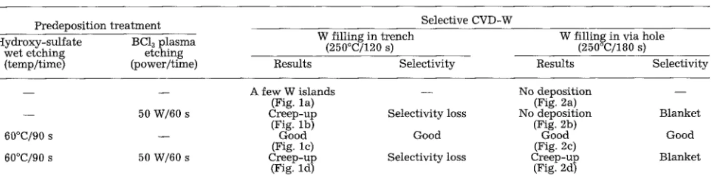
Vol. 142, No. 10, October 1995 9 The Electrochemical Society, Inc. 3585Fig. 1. Top view SEM micrographs showing selective CVD-W in submicron trenches with various precleans of substrate: (a) without any
precleaning; (b) with 50 W BCI3 plasma etching; (c) with hydroxylamine sulfate wet etching; and (d) with wet etching of (c) followed by plasma
etching of (b).
ing w a s c o n d u c t e d with a radio frequency (RF) p o w e r of 0 to i00 W, a BCI3 flow rate of i00 sccm, a n d a c h a m b e r pressure of 6 mTorr. A post-plasma-etch annealing at 370~ for 180 s w a s p e r f o r m e d to eliminate such by-products as AICI3 f r o m the a l u m i n u m surface. T h e wafers w e r e then transferred f r o m the p l a s m a etching c h a m b e r to the depo- sition c h a m b e r without exposure to atmosphere. T h e base pressure of the C V D c h a m b e r w a s i0 6 Torr. Typical condi- tions for the selective C V D - W in this w o r k w e r e as follows: substrate temperature 250~ total gas pressure 6 mTorr, W F 6 flow rate 20 seem, a n d SiH~ flow rate i0 sccm.
T h e thickness of the W plugs w a s d e t e r m i n e d b y scan- ning electron m i c r o s c o p y (SEM). Via resistance w a s m e a s - ured using the four-terminal Kelvin structure p r e p a r e d b y the conventional very large scale integrated (VLSI) pro- cessing w h e r e the via holes w e r e 0.6 I*m deep a n d 1.2 to 5 ~ m in diameter.
Results and Discussion
Trench patterns.--Selective
W d e p o s i t i o n in s u b m i c r o n t r e n c h e s w i t h a l u m i n u m at t h e b o t t o m w i t h v a r i o u s p r e - cleans w a s i n v e s t i g a t e d ; t h e results are s u m m a r i z e d in Table I. W i t h o u t a n y p r e c l e a n , W c a n n o t be d e p o s i t e d easily on t h e a l u m i n u m s u r f a c e b e c a u s e t h e a l u m i n u m o x i d e re- t a r d s t h e n u c l e a t i o n of W; thus, o n l y a f e w W islands w e r e deposited, as s h o w n in Fig. l a . W i t h a 50 W BC13 p l a s m a e t c h i n g for 60 s, c r e e p - u p a n d s e l e c t i v i t y loss of W d e p o s i - t i o n w a s o b s e r v e d , as s h o w n in Fig. l b . This is b e l i e v e d to be due to t h e o u t s p u t t e r e d a l u m i n u m o x i d e a n d a l u m i n u m i n d u c e d W n u c l e a t i o n on t h e s i d e w a l l s of t r e n c h e s a n d t h e s u r f a c e of t h e d i e l e c t r i c layer. T h e s e l e c t i v i t y loss b e c o m e s w o r s e w i t h p r o l o n g e d d e p o s i t i o n(e.g.,
180 s or longer). P l a s m a e t c h i n g w i t h h i g h e r p o w e r r e s u l t e d in m o r e severe c r e e p - u p d e p o s i t i o n a n d s e l e c t i v i t y loss. W h e n t h e w a f e r s w e r e t r e a t e d w i t h BC13 w i t h o u t t u r n i n g on t h e R F p o w e r to g e n e r a t e a p l a s m a , it was h a r d to d e p o s i t W on t h e a l u - m i n u m . Apparently, t h e a l u m i n u m o x i d e in t h e t r e n c h c a n - n o t be r e m o v e d b y BC13 alone. T h e selectivity of C V D - W c a n be i m p r o v e d significantly b y precleaning the substrate w a f e r in a h y d r o x y l a m i n e sul- fate solution, w h i c h is p r e s u m a b l y capable of completely r e m o v i n g the a l u m i n u m - oxide in the s u b m i c r o n a l u m i n u m trench. After the h y d r o x y l a m i n e sulfate w e t etching, excel- lent selective W deposition on the s u b m i c r o n a l u m i n u m trench can be obtained, as s h o w n in Fig. ic. N o selectivity loss or creep-up of W w a s found. To investigate the effect of BCI3 p l a s m a treatment, a w a f e r that h a d b e e n etched in the solution of h y d r o x y l a m i n e sulfate w a s loaded into a p l a s m a c h a m b e r for a BCI3 p l a s m a etching prior to conducting the C V D - W . After w e t etching a n d l o w p o w e r (50 W ) p l a s m a etching, selective deposition of W in the a l u m i n u m trench can be obtained, as s h o w n in Fig. Id. C r e e p - u p a n d selec- tivity loss of W deposition w e r e observed, apparently be- cause a l u m i n u m particles w e r e outsputtered b y the BCI3 plasma. It is clear f r o m the a b o v e observation that the p l a s m a etching induces the creep-up a n d selectivity loss during W deposition.Via patterns.--Selective
W d e p o s i t i o n on s u b m i c r o n via holes d o w n to A1 w i t h v a r i o u s p r e c l e a n s w a s i n v e s t i g a t e d , a n d t h e results a r e s u m m a r i z e d in Table I. C o m p a r e d to t h e s e l e c t i v e W filling of trenches, it is m o r e difficult to c o n t r o l t h e s e l e c t i v i t y loss f o r t h e W filling of v i a holes. W i t h o u t a p r e c l e a n , W d i d n o t n u c l e a t e in t h e s u b m i c r o n via, as) unless CC License in place (see abstract).
ecsdl.org/site/terms_use
address. Redistribution subject to ECS terms of use (see
140.113.38.11
3586
J. Electrochem. Soc.,
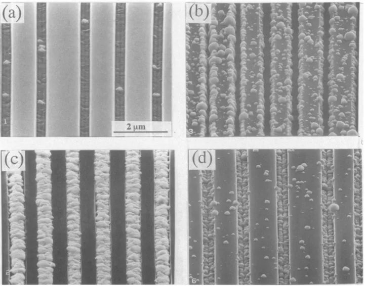
Vol. 142, No. 10, October 1995 9 The Electrochemical Society, Inc.Fig. 2. Cross-sectional SEM micrographs showing CVD-W in submicron via holes with various precleans of substrate: (a) without any
precleaning, (b) with 50 W BCI3 plasma etching; (c) with hydroxylamine sulfate wet etching; and (d) with wet etching of (c) followed by plasma
etching of (b).
shown in Fig. 2a. The belly-shaped via is due to the differ- ent etching rate b e t w e e n SOG and PECVD oxide during the via etching. With a 50 W BC13 plasma t r e a t m e n t for 60 s, blanket W deposition was obtained with practically no deposition of W in the via hole, as shown in Fig. 2b. This is different from the trench result (Fig. lb) where a larger aluminum surface is exposed. On the substrate containing via holes, p l a s m a - g e n e r a t e d a l u m i n u m particles induced W nucleation first on the surface of S i Q and around the via mouths, whereas no deposition of W inside the via hole was possible. To clarify the cause of selectivity loss, a blanket oxide-covered wafer was loaded into the CVD-W system for an in s i t u BC13 plasma cleaning followed by CVD-W deposition. No deposition of W on the oxide surface was observed. This indicates that the loss of selectivity is not due to possible damage of the oxide by the plasma. The selectivity loss presumably is due to outsputtered alu- m i n u m particles.
Precleaning the wafer in a solution of hydroxylamine sulfate significantly improved the selectivity of CVD-W and resulted in a full W filling on via holes, as shown in Fig. 2c. When the preclean was followed by a low power (50 W) plasma etching p r i o r to conducting the CVD-W, the CVD-W resulted in creep-up and blanket deposition of W, as shown in Fig. 2d. From the above observation, it is clear that the aluminum oxide in the submicron via was removed sufficiently to allow W nucleation by the hydroxylamine sulfate solution, but the subsequent plasma etching pre- sumbly outsputtered the aluminum particles and had them redeposited on the surface of S i Q . For the wet clean in the solution of hydroxylamine sulfate, it was found that the optimum condition is to wet etch at 60~ for 90 s. In s i t u ultrasonic agitation is necessary for completely cleaning the submicron via as well as to ensure a uniform W deposi- tion. L o w resistivity (--13 ~Y~-cm) tungsten film w a s selec-
tively deposited on 0.6 ~ m vias with a deposition rate of 330 nm/min. At the beginning of W deposition, W was nu- cleated from the bottom of submicron via holes, as s h o w n in Fig. 3a, leading to m a n y large islands. These islands merge together, finally resulting in the W plug with a rough surface, as shown in Fig. 3b. Figure 3c shows a cross-sec- tional micrograph of W plug with a smooth W/A1SiCu interface.
C h e m i c a l c h a r a c t e r i z a t i o n . - - H y d r o x y l a m i n e sulfate [(NH2OH)2 9 H~SO4] is a powerful reducing agent capable of removing a l u m i n u m oxide (A1203). We proposed the overall process as follows. Since hydroxylamine (NH2OH) may be thought of as being derived from NH~ by the replacement of one hydrogen by OH, it is a weaker base than NH3 and can be easily dissolved in w a t e r 9
NH~OH(aq) + H~O --> NH3OH § + OH [1] When the aluminum via p a t t e r n e d w a f e r is immersed in the solution of hydroxylamine sulfate, the aluminum oxide (A1203) and/or a l u m i n u m at the bottom of the via hole un- dergoes the following reaction 1~
A1, or A1203 + OH- -~ AI(OH)3(s) [2] Thus, the hydroxylamine sulfate solution w i t h the concen- tration of 0.1 M etches the a l u m i n u m to some extent. The aluminum consumption is dependent on the t e m p e r a t u r e and concentration of the solution. Figure 4 shows alu- m i n u m consumption vs. etching time in a solution of hy- droxylamine sulfate w i t h the concentration of 0.1 M at two different ambient temperatures. About 45 nm of A1 was removed by 60 s of etching at 60~ The reaction by-product AI(OH)3(~ ~ was precipitated in a h y d r a t e d form as a white gelatinous mass that is soluble in acid I~
) unless CC License in place (see abstract).
ecsdl.org/site/terms_use
address. Redistribution subject to ECS terms of use (see
140.113.38.11
J. Electrochem. Soc.,
Vol. 142, No. 10, October 1995 9The Electrochemical Society,
Inc. 3587AI(OH)3(, ) + 3H + --> Al 3+ (aq) +3H20(I) [3]
where the H + ion was contributed by H2SO4 in the hydroxy- lamine sulfate solution. In this way, the native a l u m i n u m oxide can be completely removed by the hydroxylamine sulfate solution. The deionized water rinse is necessary for removing the by-produc~s of this reducing reaction.
Electrical and physical characterization.--Via resist- ance was measured using a four-terminal Kelvin structure of A1SiCu/W/A1SiCu. Figure 5 illustrates the measured via resistance vs. via size for two different etching treatments
2
1 0 0 8 0 6 0 4 0 2 0<
0 0 | I I I6 ~ 1 7 6
f J J /9
z J 9 I I I I 2 4 6 8Etching Time (min.)
Fig. 4. Aluminum consumption vs,
etching time of hydroxylamine
sulfate solution at temperatures of 40 and 60~
prior to CVD-W. At least 20 r a n d o m l y chosen samples were measured in each case. The slightly higher via resistance for the sample treated with the hydroxylamine sulfate wet etching presumably is due to the reoxidation of the alu- m i n u m surface during the short time when the sample was exposed to the air before loading into the W deposition chamber.
Comparison was made on secondary ion mass spectro- scopic (SIMS) depth profiles measured on CVD-W de- posited on the a l u m i n u m substrate with a n d without pre- cleans. Without precleaning, the depth profile of high a l u m i n u m a n d oxygen concentration in the surface region, as shown i n Fig. 6a, indicates the presence of a l u m i n u m oxide; apparently no W film was deposited on the alu- minum. It can be seen from Fig. 6b that the a l u m i n u m oxide was removed a n d a W film was deposited on the sample with 30 W BC13 plasma etching. Similar results were ob- tained for the sample precleaned with the hydroxylamine sulfate solution, as shown in Fig. 6c. The high concentra- tion of fluorine at the a l u m i n u m / t u n g s t e n interface is pre- sumably due to the A1F3 compound that is formed during CVD-W. ~2'13 At the same deposition time of CVD-W, com- parsion between Fig. 6b a n d c indicates that a thicker W film was deposited on the substrate that was precleaned using BC13 plasma etching; this presumably is due to the
Fig. 3. (a) Cross section, (b) top view, and (c) cross-sectional SEM
micrographs showing CVD-W filling in submicron via pretreated with
hydroxylamine sulfate wet etching.
3.5
~ - ~3.0
,~
2.5
..~
.~ 2.0
>
! !e. wet etching.
. . . . m g" 9
1 . 5 , I , I ,0
10
20
30
Via Size (~m 2)
Fig. 5. Via resistance vs.
via size with precleans of 50 W BCI3
plasma etching and hydroxylamine sulfate wet etching.
) unless CC License in place (see abstract).
ecsdl.org/site/terms_use
address. Redistribution subject to ECS terms of use (see
140.113.38.11
3588
d. Electrochem. Soc.,
Vol. 142, No. 10, October 1995 9 The Electrochemical Society, Inc.
105
9 ~ 10 4 ~10 ~
10 2
r--,o
L)
101
! ! ! io., ol
Ai( a )
w
lo 0
0
0.1
0.2
0.3
0.4
0.5
Depth (~tm)
105
i
BCl, plasma
I
!
!
|etching
A]
( b )
" ~
104
... =
. . .
p ~&~
10
~ 1 0 3 ~ F ~
,.
lo'
!
10 o
0
0.1
0.2
0.3
0.4
0.5
Depth (/.tm)
.6
c :o
O
10 s
10 4
10 3
10 2
10'
10 0
0
Hydro-lsulfate Jet etching AI ' (C) 1
0.1
0.2
0.3
0.4
0.5
Depth (gin)
Fig. 6. SIMS depth profiles of 60 s CVD-W deposition on aluminum
substrates (a) without any precleaning; (b) with 30 W BCI3 plasma
etching; and (c) with dilute hydroxylamine sulfate wet etching.
p l a s m a - g e n e r a t e d surface damage on A1, which can easily induce W nucleation on the d a m a g e d sites.
Conclusion
Precleaning of the aluminum trench and via p a t t e r n e d s u b s t r a t e is vital to the successful selective CVD-W. As to BC13 p l a s m a etching precleaning, we found t h a t the out- sputtered aluminum oxide a n d / o r a l u m i n u m can be rede- posited on the sidewall of the trench and via hole, as well as on the surface of the S i Q . This resulted in creep-up and selectivity loss d u r i n g the subsequent selective CVD-W. Excellent selective CVD-W can be obtained using the hy- droxylamine sulfate solution to p r e t r e a t the trench and via p a t t e r n e d substrate; this precleaning completely removes the metal oxide at the b o t t o m of aluminum trench a n d via. Thus, creep-up and selectivity loss of W deposition can be avoided.
Acknowledgment
This w o r k was s u p p o r t e d b y the N a t i o n a l Science Coun- cil (ROC) under Contract No. NSC84-2622-E009-007-1.
Manuscript s u b m i t t e d March 14, 1995; revised m a n u - script received June 6, 1995.
National Chiao Tung University assisted in meeting the publication costs of this article.
REFERENCES
1. R. H. Wilison, R. W. Stall, and M. A. Calacone, VLSI Multilevel Interconnection Conference, IEEE, p. 343, New York (1985).
2. D. M. Brown, B. Horowitz, R Piacente, R. Sara, R. Wilson, and D. Woodruff, IEEE Electron Device Lett., EDL-8, 55 (1987).
3. C. Kaanta, W Cote, J. Cronin, K. Holland, P. 1. Lee, and T. Wright, IEEE IEDM, Tech. Digest, 218 (1987). 4. J. E. J. Schmitz, Chemical Vapor Deposition of Tung-
sten and Tungsten Silicide, pp. 75-80, Noyes P u b l i c a - tions, P a r k Ridge, NJ (1992).
5. D. L. Flamm, Solid State TechnoI., 37 (August, 1992). 6. S. F u j i m u r a and H. Yano, This Journal, 135, 1195
(1988).
7. D.R. Broadbury, J. E. Turner, K. Nauka, and K. Y. Chiu, IEEE IEDM Tech. Digest, 273 (1991).
8. R E. Riley, S. S. Peng, and L. Fang, Solid State Tech- nol., 47 (Feb. 1993).
9. E A. Cotton a n d G. Wilkinson, Advanced Inorganic Chemistry, pp. 319-320, John Wiley & Sons, New York (1988).
10. F. A. Cotton and G. Wilkinson, Basic Inorganic Chem- istry, pp. 313-314, John Wiley & Sons, New York (1987).
11. G. I. Brown, Introduction to Inorganic Chemistry, pp. 194-195, Longman-Greene, London (1985). 12. M. L. Yu, K. Y. Ahn, and R. V. Joshi, J. Appl. Phys., 67,
1055 (1990).
13. H. Ohsima, M. K a t a y a m a , K. Onoa, and T. Hatori, This Journal, 140, 801 (1993).
) unless CC License in place (see abstract).
ecsdl.org/site/terms_use
address. Redistribution subject to ECS terms of use (see
140.113.38.11