Growth of very-high-mobility Al Ga Sb In As high-electron-mobility transistor structure
on si substrate for high speed electronic applications
Y. C. Lin, H. Yamaguchi, E. Y. Chang, Y. C. Hsieh, M. Ueki, Y. Hirayama, and C. Y. Chang
Citation: Applied Physics Letters 90, 023509 (2007); doi: 10.1063/1.2431567 View online: http://dx.doi.org/10.1063/1.2431567
View Table of Contents: http://scitation.aip.org/content/aip/journal/apl/90/2?ver=pdfcov
Published by the AIP Publishing
Articles you may be interested in
In As Al Sb high-electron-mobility transistors by molecular-beam epitaxy for low-power applications
J. Vac. Sci. Technol. B 24, 2581 (2006); 10.1116/1.2362758
Correlation between optical and electrical properties in In 0.52 Al 0.48 As In x Ga 1 x As metamorphic high-electron-mobility-transistor structures on GaAs substrates
J. Appl. Phys. 100, 033705 (2006); 10.1063/1.2222404
Influence of silicon nitride passivation on transport properties in In Al As In Ga As In P composite channel high electron mobility transistor structures
J. Vac. Sci. Technol. B 24, 1711 (2006); 10.1116/1.2209989
Terahertz plasma wave resonance of two-dimensional electrons in In Ga P In Ga As Ga As high-electron-mobility transistors
Appl. Phys. Lett. 85, 2119 (2004); 10.1063/1.1792377
Improved characteristics of metamorphic In Al As In Ga As high electron mobility transistor with symmetric graded In x Ga 1 x As channel
J. Vac. Sci. Technol. B 22, 2429 (2004); 10.1116/1.1781662
This article is copyrighted as indicated in the article. Reuse of AIP content is subject to the terms at: http://scitation.aip.org/termsconditions. Downloaded to IP: 140.113.38.11 On: Thu, 01 May 2014 00:41:53
Growth of very-high-mobility AlGaSb/ InAs high-electron-mobility transistor
structure on si substrate for high speed electronic applications
Y. C. Lin
Department of Materials Science and Engineering, National Chiao Tung University, Taiwan 30050, Republic of China and NTT Basic Research Laboratories, Kanagawa 243-0198, Japan
H. Yamaguchi
NTT Basic Research Laboratories, Kanagawa 243-0198, Japan and Department of Physics, Tohoku University, Sendai 980-8578, Japan
E. Y. Changa兲and Y. C. Hsieh
Department of Materials Science and Engineering, National Chiao Tung University, Taiwan 30050, Republic of China
M. Ueki
NTT Electronics Techno Corporation, Kanagawa 221-0052, Japan Y. Hirayama
NTT Basic Research Laboratories, Kanagawa 243-0198, Japan; Department of Physics, Tohoku University, Sendai 980-8578, Japan; and SORST-JST, Saitama 331-0012, Japan
C. Y. Chang
Department of Electronic Engineering, National Chiao Tung University, Taiwan 30050, Republic of China 共Received 11 October 2006; accepted 12 December 2006; published online 11 January 2007兲 The growth of the AlGaSb/ InAs high-electron-mobility transistor共HEMT兲 epitaxial structure on the Si substrate is investigated. Buffer layers consisted of UHV/chemical vapor deposited grown Ge/ GeSi and molecular beam epitaxy-grown AlGaSb/ AlSb/ GaAs were used to accommodate the strain induced by the large lattice mismatch between the AlGaSb/ InAs HEMT structure and the Si substrate. The crystalline quality of the structure grown was examined by x-ray diffraction, transmission electron microscopy, and atomic force microscopy. Finally, very high room-temperature electron mobility of 27 300 cm2/ V s was achieved. It is demonstrated that a
very-high-mobility AlGaSb/ InAs HEMT structure on the Si substrate can be achieved with the properly designed buffer layers. © 2007 American Institute of Physics.关DOI:10.1063/1.2431567兴
Integration of III-V semiconductors on Si substrates has been investigated for microwave and millimeter-wave de-vices and monolithic integrated circuits in the past.1–5 Re-cently, the growth of compound semiconductor heterostruc-tures on Si substrates has attracted continuous attention because of the possible integration of III-V device on Si substrates for logic applications. The use of GaAs-on-Si to replace GaAs substrate has the following advantages: high thermal conductivity, potential wafer-size expansion, me-chanical hardness of substrates, and lower cost for Si substrates.5–7 For high speed electronic applications, anti-mony共Sb兲-based high-electron-mobility transistors 共HEMTs兲 with InAs channel layer have been studied in recent years.8–12The InAs layer was chosen as the channel material for the HEMT due to its high electron mobility and high quantum confinement in the channel region. In this letter, the growth of the Al0.5Ga0.5Sb/ InAs HEMT on Si substrate for
high speed electronic application is studied.
There are two problems to be overcome for the growth of high-quality Al0.5Ga0.5Sb/ InAs HEMT epitaxial layers on
Si substrate. One is the strain induced by the large lattice mismatch of 11% between the Al0.5Ga0.5Sb/ InAs HEMT structure and the Si substrate, the other is the residual stress due to the large difference in the thermal expansion coeffi-cients of these two material systems.13To obtain high quality the Al0.5Ga0.5Sb/ InAs HEMT on Si, two buffer layers of
Ge/ Ge0.95Si0.05/ Ge0.9Si0.1, and Al0.5Ga0.5Sb/ AlSb/ GaAs were used. First, the Ge/ Ge0.95Si0.05/ Ge0.9Si0.1 layer was
used as the buffer layer for the growth of GaAs on Si sub-strate, because Ge and GaAs have similar lattice constants and thermal expansion coefficients.13 Then, the Al0.5Ga0.5Sb/ AlSb layers were grown to accommodate the
strain induced by the large lattice mismatch between the Al0.5Ga0.5Sb/ InAs system and the GaAs layer.10The
crystal-line quality of the Al0.5Ga0.5Sb/ InAs HEMT structure grown
on Si was analyzed by X-ray diffraction analysis, transmis-sion electron microscopy共TEM兲, and atomic force micros-copy共AFM兲. The thickness of the epitaxial layers, the dislo-cation distribution, and the threading dislodislo-cation density were evaluated using the above analytical tools. A very high room-temperature electron mobility of 27 300 cm2/ V s and a sheet density of 3.04⫻1012/ cm2 for the Al
0.5Ga0.5Sb/ InAs
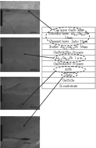
HEMT structure grown on the Si substrate were obtained. The Al0.5Ga0.5Sb/ InAs structure grown on Si is shown in
Fig.1. A Si共100兲 substrate wafer with 6° off-cut toward the 关110兴 direction and three epitaxial growth systems were used for the growth of the Al0.5Ga0.5Sb/ InAs HEMT structure on
Si in this study. First, an ultrahigh vacuum chemical vapor deposition 共CVD兲 system was used to grow the Ge/ Ge0.95Si0.05/ Ge0.9Si0.1layers. Then, a thin GaAs film was grown by a commercial metal organic chemical vapor depo-sition 共MOCVD兲.13 Finally, the Al0.5Ga0.5Sb/ InAs HEMT structure was grown by a molecular beam epitaxy 共MBE兲 system.
a兲Electronic mail: edc@mail.nctu.edu.tw
APPLIED PHYSICS LETTERS 90, 023509共2007兲
0003-6951/2007/90共2兲/023509/3/$23.00 90, 023509-1 © 2007 American Institute of Physics
This article is copyrighted as indicated in the article. Reuse of AIP content is subject to the terms at: http://scitation.aip.org/termsconditions. Downloaded to IP: 140.113.38.11 On: Thu, 01 May 2014 00:41:53
For the Ge/ Ge0.95Si0.05/ Ge0.9Si0.1 layer growth, the Si substrate was first cleaned by 10% HF dipping and then went through high-temperature baking at 800 ° C in the growth chamber for 5 min. Then, a 0.8m Si0.1Ge0.9 layer, a
0.8m Si0.05Ge0.95layer, and a 1.0 m Ge layer were grown
at 400 ° C in sequence on the Si wafer as the buffer layer.13 After that, a 1.5m GaAs layer was grown on Ge at a tem-perature of 600 ° C by MOCVD. The growth conditions of GaAs are as follows: growth pressure is 40 torr, V/III ratio is 100, and growth rate is 1.7m / h.13 Finally, the Al0.5Ga0.5Sb/ InAs HEMT was grown on top of the Ge layer by MBE system and the wafer was baked at 630 ° C for 1 min before the growth. The growth of the Al0.5Ga0.5Sb/ InAs HEMT structure can be divided into two
major parts: buffer layer growth and InAs channel layer growth. The growth of the buffer layers includes a GaAs layer, an AlSb layer, two GaSb/ AlSb supperlattice, and two Al0.5Ga0.5Sb layers; the buffer layers were grown before the
channel region to accommodate the 7% lattice mismatch be-tween the Al0.5Ga0.5Sb/ InAs HEMT structure and the Ge layer. The growth temperature of the buffer layers was set at 560 ° C. A 1m GaAs layer was grown on Ge first. After that, a 100 nm AlSb layer, a superlattice of 50 nm with ten pairs of GaSb/ AlSb, and a 1m Al0.5Ga0.5Sb were grown
layer by layer. Then, 50 nm GaSb/ AlSb superlattice 共ten pairs兲, a 50 nm Al0.5Ga0.5Sb layer, a 15 nm InAs layer, a
13 nm Al0.5Ga0.5Sb layer, and a 3 nm GaSb layer were
grown. To obtain good quality InAs channel layer, the growth temperature was set at 520 ° C after the growth of the Al0.5Ga0.5Sb layer. The growth rate of InAs channel layer was 1.5 Å / s, and the 13 nm Al0.5Ga0.5Sb layer and the 3 nm
GaSb layer are the Schottky layer and the cap layer, respec-tively. The Al0.5Ga0.5Sb/ InAs HEMT on Si structure grown
is shown in Fig.1.
We have reported the use of SiGe buffer layer for the growth of Ge on top of Si substrate before.13 Because the Ge/ Ge0.95Si0.05/ Ge0.9Si0.1interface can be used to
accommo-date the strain induced by the large lattice mismatch, the upwardly propagated dislocations were bent sideward and terminated very effectively at the Si0.05Ge0.95/ Si0.1Ge0.9and
Ge/ Si0.05Ge0.95 interfaces. Almost no threading dislocation
can propagate into the top Ge layer.13 Figure 2 shows the cross-sectional TEM images of the Al0.5Ga0.5Sb/ InAs HEMT on Ge with SiGe buffer layer, the interfaces of buff-ers were quite smooth as shown in this figure. Figure3
pre-sents the TEM micrograph of the InAs layer. As can be seen in this figure, the defect density in the InAs layer was very low.
The surface roughness of the Al0.5Ga0.5Sb/ InAs HEMT
grown on Si wafer was compared to the Al0.5Ga0.5Sb/ InAs
HEMT structure grown on the GaAs substrate. Figure4 pre-sents the AFM images of the two different substrate wafers. No cross-hatching patterns were observed on the wafer sur-face. The root mean square共rms兲 of the Al0.5Ga0.5Sb/ InAs
HEMT on Si wafer surface was 19.1 Å, in comparison with
FIG. 1. Structure of the AlGaSb/ InAs HEMT grown on the Si substrate.
FIG. 2. Cross section of the TEM images of the AlGaSb/ InAs HEMT on Si substrate.
FIG. 3. Cross section of the TEM images of the InAs layer in the AlGaSb/ InAs HEMT grown on Si substrate.
023509-2 Lin et al. Appl. Phys. Lett. 90, 023509共2007兲
This article is copyrighted as indicated in the article. Reuse of AIP content is subject to the terms at: http://scitation.aip.org/termsconditions. Downloaded to IP: 140.113.38.11 On: Thu, 01 May 2014 00:41:53
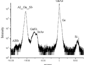
rms of 15.5 Å for the surface of Al0.5Ga0.5Sb/ InAs HEMT on GaAs substrate wafer. Figure 5 is the x-ray diffraction curve of the Al0.5Ga0.5Sb/ InAs HEMT structure on Si
sub-strate wafer. The diffraction pattern has seven major peaks and was identified as GaAs, Ge, Si, AlGaSb, InAs, AlSb, and GaSb peaks, respectively. It indicates that the crystalline quality of the HEMT epitaxial layers is very good. Very high room-temperature electron mobility of 27 300 cm2/ V s and a sheet density of 3.04⫻1012/ cm2 were measured for the
Al0.5Ga0.5Sb/ InAs HEMT structure grown on the Si
sub-strate due to the high-quality epitaxial layers grown. It is demonstrated that a very-high-mobility Al0.5Ga0.5Sb/ InAs
HEMT structure can be grown on Si substrate with properly designed Al0.5Ga0.5Sb/ AlSb/ GaAs and SiGe buffer layers.
The growth of the Al0.5Ga0.5Sb/ InAs HEMT structure on Si substrate is reported in this letter. We have designed an Al0.5Ga0.5Sb/ AlSb/ GaAs and SiGe buffer structures for the
growth of the high-quality Al0.5Ga0.5Sb/ InAs HEMT
struc-ture on the Si substrates. The cross-sectional TEM images of the AlGaSb/ InAs HEMT on Ge show very smooth interfaces of the structure grown and low defect density InAs channel layer. The AFM images of the wafer show no cross-hatching pattern and bending on the wafer surface. The root mean square 共rms兲 of the surface roughness of the Al0.5Ga0.5Sb/ InAs HEMT on Si wafer surface was 19.1 Å.
The x-ray diffraction patterns of the Al0.5Ga0.5Sb/ InAs HEMT structure on Si substrate wafer exhibited clearly seven major peaks and the diffracted peaks indicated that the crystalline quality of the HEMT structure was very good. The room-temperature electron mobility of 27 300 cm2/ V s
and a sheet density of 3.04⫻1012/ cm2were achieved for the
Al0.5Ga0.5Sb/ InAs HEMT grown on Si substrate using
Ge/ Ge0.95Si0.05/ Ge0.9Si0.1 as the buffer layer. This is the
highest mobility for a HEMT structure grown on Si substrate reported so far and we have demonstrated that a very-high-mobility Al0.5Ga0.5Sb/ InAs HEMT structure can be grown on Si substrate if the buffer layers are properly designed.
This work was supported in JSPS KAKENHI 共16206003兲 and the Ministry of Education and the Ministry of Economic Affairs and the National Science Council of Taiwan of the Republic of China for supporting this research under contract Nos. NSC 2752-E-009-001-PAE and 94-EC-17-A-05-S1-020.
1Guang-bo Gao, Zhi-fang Fan, D. L. Blackburn, M. S. Ünlü, J. Chen, K.
Adomi, and H. Morkoc, Appl. Phys. Lett. 58, 1068共1991兲.
2Kai Ma, Ray Chen, David A. B. Miller, and James S. Harris, Jr., IEEE J.
Sel. Top. Quantum Electron. 11, 1278共2005兲.
3Alexandros Georgakilas, George Halkias, Aris Christou, Christos
Papavassiliou, George Perantinos, George Konstantinidis, and Paul N. Panayotatos, IEEE Trans. Electron Devices 40, 507共1993兲.
4Toshiki Makimoto, Kenji Kurishima, Takashi Kobayashi, and Tadao
Ishibashi, IEEE Electron Device Lett. 12, 369共1991兲.
5Mitsuhiko Goto, Yasumitsu Ohta, Takashi Aigo, and Akihiro Moritani,
IEEE Trans. Microwave Theory Tech. 44, 668共1996兲.
6K. Ohtsuka and H. Nakanishi, Proceedings of the 19th International
Sym-posium on Gallium Arsenide and Related Compounds 共unpublished兲, p. 881.
7T. Aigo, H. Yashiro, A. Jono, A. Tachikawa, and A. Moritani, Electron.
Lett. 28, 1737共1992兲.
8J. Brad Boos, Walter Kruppa, Brian R. Bennett, Doewon Park, Steven W.
Kirchoefer, Robert Bass, and Harry B. Dietrich, IEEE Trans. Electron Devices 45, 1869共1998兲.
9N. A. Papanicolaou, B. R. Bennet, J. B. Boos, D. Park, and R. Bass,
Electron. Lett. 41, 1088共2005兲.
10Kanji Yoh, Toshiaki Moriuchi, and Masataka Inoue, IEEE Electron Device
Lett. 11, 526共1990兲.
11C. R. Bolognesi, E. J. Caine, and H. Kroemer, IEEE Electron Device Lett.
15, 16共1994兲.
12R. Tsai, M. Barsky, J. Lee, J. B. Boos, B. R. Bennett, R. Magno, C.
Namba, P. H. Liu, A. Gutierrez, and R. Lai, IEEE Lester Eastman Conference, 2002, p. 276.
13Edward Yi Chang, Tsung-His Yang, Guang-Li Luo, and Chun-Yen Chang,
J. Electron. Mater. 34, 23共2005兲.
FIG. 5. Double crystal x-ray diffraction patterns of the AlGaSb/ InAs HEMT on Si substrate.
FIG. 4. Surface morphology of 共a兲 the AlGaSb/InAs HEMT structure grown on Si substrate and共b兲 the AlGaSb/InAs HEMT structure grown on GaAs substrate.
023509-3 Lin et al. Appl. Phys. Lett. 90, 023509共2007兲
This article is copyrighted as indicated in the article. Reuse of AIP content is subject to the terms at: http://scitation.aip.org/termsconditions. Downloaded to IP: 140.113.38.11 On: Thu, 01 May 2014 00:41:53