Highly Oriented (Zr
0.7Sn
0.3)TiO
4Thin Films Grown by
rf Magnetron Sputtering
Fang-Jy Wu and Tseung-Yuen Tseng
* Department of Electronics Engineering and Institute of Electronics, National Chiao Tung University, Hsinchu, Taiwan, Republic of ChinaThin films of (Zr0.7Sn0.3)TiO4on Si(100) were prepared by rf magnetron sputtering in the present study. Films of a highly preferred [020] orientation, as demonstrated by X-ray diffraction and transmission electron microscopic ex-aminations, were grown successfully on a Si substrate with in situ postannealing at 700°C. The chemical composition of the films, measured by secondary ion mass spectroscopy, exhibited a uniform concentration distribution for all spe-cies. A study by X-ray photoelectron spectroscopy further revealed some firm evidence of a molecular orbital that affected the chemical structure. The dielectric constants of 400-nm-thick (Zr0.7Sn0.3)TiO4 films in the present study were >18 for the films with a preferred orientation and∼11 for polycrystalline films.
I. Introduction
Z
IRCONIUM TIN TITANIUM OXIDEbulk ceramics, which are di-electric ceramics of interest for their role in the resonator components of microwave devices, have won a prominent po-sition in microwave communications systems.1,2 Ceramics based on the solid solution (Zr1−xSnx)TiO4, with up to 20 at.% of the Zr replaced by Sn, have been used as resonator materials since the 1970s.3 Systematically varying the composition within the solid-solution region has produced ceramic dielec-trics with selective temperature coefficients of the dielectric constant and resonant frequency, a requirement for specific device applications.4Much research and study have been de-voted to (Zr0.7Sn0.3)TiO4(ZST) bulk ceramic properties. Solid-solution formation in the system ZrO2–TiO2–SnO2 has been investigated, and single-phase solid solutions of SnO2 in Zr-TiO4 have been located in the zone for the composition Zrx-SnyTizO4.5
Strong interaction forces between the ions in ZrTiO4 are weakened in solid solutions because of the decreasing number of interacting ions in the case of (Zr1−xSnx)TiO4, and the
di-electric properties of ZrTiO4ceramics have been improved by incorporating SnO2.6ZST reportedly has a dielectric constant of 38, a much larger value than that of SiO2. Thin films of ZST therefore can be regarded as an additional kind of dielectric material for charge storage in 256 Mbit dynamic random access memories (DRAMs).
So far, the microstructure and electrical properties of rf-sputtered (Zr1−xSnx)TiO4 thin films have been studied little.
The present researchers have prepared ZrTiO4thin films on Si substrates by rf sputtering deposition, and the physical and
electrical properties of those thin films have been reported.7–9 In this work, ZST thin films on Si substrates were prepared by rf magnetron sputtering from room temperature to 600°C and
in situ annealed. The present aim was to investigate the effect
of deposition temperature and to study the structure and dielec-tric constants of ZST thin films.
II. Experimental Procedure (1) (Zr0.7Sn0.3)TiO4Thin Film Preparation
The target composition of (Zr0.7Sn0.3)TiO4was synthesized via a conventional solid-state reaction. Starting powders of high-purity (<99%) ZrO2, SnO2, and TiO2(Merck Chemicals, Inc., Germany) were weighed, placed in polypropylene con-tainers, and milled with zirconia milling media for 24 h in a waterless alcohol solution. The mixture was oven dried at 80°C, then thoroughly milled before it was calcined at 1400°C for 8 h. The calcined powder was pressed into disks measuring 5.08 mm in diameter and 3 mm thick. Each disk was sintered at 1580°C for 8 h and examined by X-ray powder diffraction (XRD), which revealed that all of the targets represented a single orthorhombic phase.10
Film deposition was performed by rf magnetron sputtering. The substrates for the present study were n-type (100)Si wafers of 4 to 7⍀䡠cm resistivity that had been chemically cleaned by standard procedures immediately prior to transfer into a vacuum chamber. All of the films were deposited at a fixed rf power level of 120 W and an operating pressure of 40 mtorr (5.33 × 10⁶Pa), a level maintained in the chamber by a mixture of Ar and O2at a flow-rate ratio of 80/20. During the deposi-tion sequence, the substrates were subjected to either ambi-ent temperature or temperatures ranging as high as 600°C in the O2/Ar mixture gas for 2 h and then maintained at 700°C for 1 h.
(2) Measurement of Structural Properties
The film structure was analyzed by XRD (Model D5000, Siemens Energy and Automation, Inc., Cherry Hill, NJ) at 50 kV and 40 mA with CuK␣ radiation. The depth profile of the film composition was analyzed by secondary ion mass spec-troscopy (SIMS) (Model IMS-4f, Cameca, France) using an O+ 2 source with an impact energy of 8 keV. The microstructure of the film was observed by transmission electron microscopy (TEM, Model 2000FX, JEOL, Ltd., Tokyo, Japan) with an accelerating voltage of 200 kV. The TEM samples were pre-pared by ion milling in the conventional manner. The film surfaces were characterized by X-ray photoelectron spectrom-etry (XPS) (Model PHI-1905ESCA, Perkin-Elmer Corp., Nor-walk, CT) with MgK␣ X-rays, and the binding energy of the spectrum was corrected by comparing it with C ls (assuming
C ⳱ 285.0 eV).11The thickness and refractive index of the films were determined by ellipsometry at 632.8 nm.
(3) Capacitance–Voltage Measurement
Metal–insulator–semiconductor (MIS) capacitors of Al/ZST/ Si structure were fabricated by depositing aluminum-top P. K. Davies—contributing editor
Manuscript No. 191413. Received November 4, 1996; approved November 19, 1997.
Supported by the National Science Council of the Republic of China under Con-tract No. NSC 85-2112-M009-037 PH.
*Member, American Ceramic Society.
Journal
electrodes on the ZST films and used for electrical mea-surements. Gold film was deposited onto the reverse side of the Si wafer to form a back contact. The C–V curves of the MIS capacitors were obtained by using the Keithly CV 82 system.
III. Results and Discussion
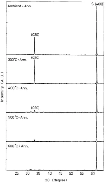
The XRD patterns of films deposited variously at ambient temperature, 300°C, and 400°C, and then annealed at 700°C for 1 h, displayed dominant (020) diffraction peaks with relatively small half-width values, as illustrated in Fig. 1. These films, of highly preferred orientation, had smooth surfaces and were transparent in visible light. Table I lists the structural properties derived from the XRD data, at various deposition temperatures, of the films together with values for d020. The spacings be-tween the (020) planes increased somewhat with increasing deposition temperature.
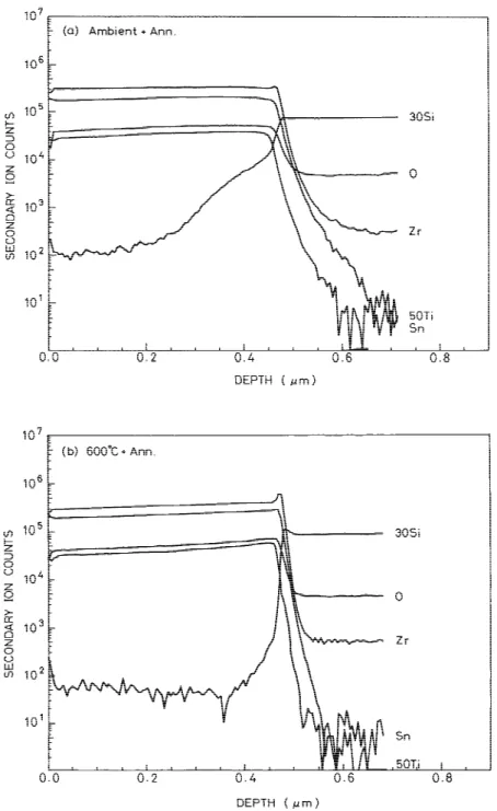
SIMS analysis yielded further insights into changes in the film chemistry caused by postannealing. The analytical finding in Figs. 2(a) and (b), which register a uniform concentration distribution for all of the cations except Si within the ZST film, represent a typical depth profile of ZST films on Si. The high level of O signal in the Si substrate of Fig. 2 does not imply a
significant concentration of oxygen in the substrate, but rather is simply an artifact of the oxygen probe used for depth pro-filing. The Si signal in the ZST film, as shown in Fig. 2(a), was apparently 3 to 4 orders of magnitude lower than that in the Si substrate. On the other hand, the Si signals for those two films demonstrate that the solubility of Si in the film deposited at ambient temperature (Fig. 2(a)) was 2.6 times (0.143%/0.55%) that in the film deposited at 600°C (Fig. 2(b)). This phenom-enon probably can be attributed to the lower packing density of the film deposited at ambient temperature. Figures 2(a) and (b) also reveal that a significant Zr diffused into the Si substrate. This diffusion is more pronounced for ZST films deposited at 600°C, less marked for the films deposited at ambient tempera-ture. A notable Zr peak observed at the interface strongly sug-gests that some part of Zr was rejected by the substrate and built up at the interface during cooling. For the present set of samples, the observed differences were simply caused by the enhanced diffusion of Si with increasing deposition tempera-ture at the film/Si-substrate interface.
To elucidate the binding energy of Si within the films, the bonding states of the films were analyzed by XPS at the surface layer. The XPS spectra of the ZST films on Si deposited at ambient temperature and at 600°C are illustrated in Fig. 3(a). The spectrum around the Si (2p) peak in Fig. 3(b) has been enlarged, with the main peaks at the higher energy known to reflect the oxidized Si (2p) level (103.0 to 103.3 eV), and the shoulder the elemental Si (2p) level (100.0 eV). XPS analysis of the ZrTiO4thin films, however, indicated that, whereas the peak position of Si lay within the region for standard Si, the oxygen peak was located outside the region for oxygen in a Si environment.8 Extremely strong peaks from the Zr (3d), Zr (3p), Sn (3d), Ti (2p), and O (ls) levels were observed, whereas the Si (2p) peaks were weak. Since the sensitivities of both the Zr (3d) and the Si (2p) are of the same order, this spectrum suggests that the bonding states of Si were the same (4+) as those of Zr in the ZST films and that Si out-diffused from the substrate into the film. A ZrSiO4solid solution thus may have formed during processing. The XPS results showed more Si in the ZST films deposited at ambient temperature, which are in good agreement with the SIMS data. It would appear that additive SnO2 tends to increase Si solubility slightly more in (Zr0.7Sn0.3)TiO4 films than in ZrTiO4 according to XPS analysis.8In addition, a splitting or shoulder of the Ti (2p) and the Sn (3d) spectra, caused by the asymmetrical atomic-arrangement effect, was noted.12Apparently, the difference in net negative charges between the oxygen ions of the two symmetrical coordinations was small, and the net negative charge of the Zr–O–Ti (and/or Sn–O–Ti) coordination ex-ceeded the symmetrical coordinations achieved by the asym-metrical atom-arrangement effect.13 The series of TEM im-ages for the films illustrated in Figs. 4(a) to (d) was extracted from planar bright-field images at deposition temperatures ranging from low to high. Figures 4(a) to (c) reveal that films deposited at 400°Cor lower possessed a highly preferred ori-entation, with smooth surfaces. At temperatures as high as 600°C, however, polycrystals with grain sizes of∼470 Å were observed.
Representative 1-MHz C–V curves of Al/(Zr0.7Sn0.3)TiO4/n-Si capacitors, formed from sputtering deposition onto Al/(Zr0.7Sn0.3)TiO4/n-Si
sub-Fig. 1. XRD patterns of (Zr0.7Sn0.3)TiO4films deposited at various temperatures and then annealed at 700°C for 1 h.
Table I. Structural Properties of the Films Deposited at Various Temperatures and Then Annealed at 700°C
Deposition temp (°C) d020(Å) Structure
Ambient 2.7118 Preferred
300 2.7118 Preferred
400 2.7141 Preferred
500 2.7154 Polycrystalline
600 2.7164 Polycrystalline
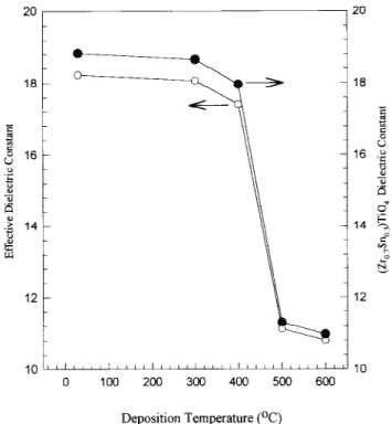
strates, are displayed in Fig. 5. The C–V curves approached ideal MIS C–V characteristics, apart from the fiat-band voltage value caused by the measuring process itself. The dielectric constants of the ZST films were calculated variously from the values of the accumulation capacitance, the known area of the aluminum counterelectrode of the MIS capacitors, and the TEM-observed oxide thickness. Those dielectric constants are plotted in Fig. 6 as a function of film deposition temperature. It indicates that the ZST film deposited at ambient temperature has a higher dielectric constant than those films deposited at higher temperatures. The difference in dielectric constants of the films is obvious. For example, the ambient ZST sample later annealed at 700°C for 1 h in O2/Ar exhibited a dielectric constant of∼18; in contrast, the sample that had been deposited at 600°C for 2 h in O2/Ar revealed a dielectric constant of∼11. In comparison with the dielectric constant of∼16.3 reported for ZrTiO4 films deposited under similar conditions (O2/Ar ra-tio⳱ 20/80), substituting SnO2for ZrO2 in the present ZST
films deposited at 400° barely increased the dielectric constant to∼17.5.8
IV. Conclusions
Homogeneous, transparent thin ZST films with uniform stoi-chiometry were grown successfully by rf magnetron sputtering. Films deposited at temperatures below 400°C onto Si sub-strates exhibited an (020) preferred orientation of adequate crystallographic-alignment quality. Silicon out-diffused from the substrate into the film. The XPS results indicated more Si in the ZST films deposited at ambient temperature than in the films deposited at 600°C, which are in good agreement with the SIMS data. The dielectric constant of ZST films proved to depend strongly on the Si substrate temperature during depo-sition. ZST films formed at a lower temperature retained di-electric constants up to 60% higher than those of films formed above 400°C.
Fig. 2. SIMS depth profile for (Zr0.7Sn0.3)TiO4film on a Si(100) substrate deposited at (a) ambient temperature and (b) 600°C, and then annealed at 700°C.
Fig. 4. TEM bright-field images of the (Zr0.7Sn0.3)TiO4films deposited at (a) ambient temperature and (b) 300°, (c) 400°, and (d) 600°C.
Fig. 3. (a) XPS spectra of (Zr0.7Sn0.3)TiO4films deposited at ambient temperature (A) and 600°C (B). (b) Expanded trace of the spectra around the Si (2p) peaks shown in Fig. 3(a).
References
1H. Tamura, ‘‘Microwave Loss Quality of (Zr
0.8Sn0.2)TiO4,’’ Am. Ceram.
Soc. Bull., 73 [10] 92–95 (1994).
2K. Wakino, T. Nishikawa, Y. Ishikawa, and H. Tamura, ‘‘Dielectric
Reso-nator Materials and Their Applications for Mobile Communication Systems,’’
Br. Ceram. Trans. J., 89 [2] 39–43 (1990).
3K. Wakino, K. Minai, and H. Tamura, ‘‘Microwave Characteristics of
(Zr,Sn)TiO4and BaO–PbO–Nd2O3–TiO2Dielectric Resonators,’’ J. Am.
Ce-ram. Soc., 67 [4] 278–81 (1984).
4S. I. Hirano, T. Hayashi, and A. Hattori, ‘‘Chemical Processing and
Micro-wave Characteristics of (Zr,Sn)TiO4Microwave Dielectrics,’’ J. Am. Ceram.
Soc., 74 [6] 1320–24 (1991).
5G. Wolfram and H. E. Gobel, ‘‘Existence Range, Structure, and Dielectric
Properties of ZrxTiySnzO4Ceramics (x + y + z⳱ 2),’’ Mater. Res. Bull., 16 [11]
1455–63 (1981).
6H. Ikawa, A. Iwai, K. Hiruta, H. Shimojima, K. Urabe, and S. Udagawa,
‘‘Phase Transformation and Thermal Expansion of Zirconium and Hafnium Titanates and Their Solid Solution,’’ J. Am. Ceram. Soc., 71 [2] 120–27 (1988).
7D. A. Chang, P. Lin, and T. Y. Tseng, ‘‘Growth of Highly Oriented ZrTiO 4
Thin Films by Radio-Frequency Magnetron Sputtering,’’ Appl. Phys. Lett., 64 [24] 3252–54 (1994).
8D. A. Chang, P. Lin, and T. Y. Tseng, ‘‘Effects of Oxygen–Argon Mixing
on the Electrical and Physical Properties of ZrTiO4Films Sputtered on Silicon
at Low Temperature,’’ J. Appl. Phys., 78 [12] 7103–108 (1995).
9D. A. Chang, P. Lin, and T. Y. Tseng, ‘‘Effects of Substrate Temperature
and Oxygen Partial Pressure on the Properties of Sputtered Zirconium Titanate Thin Films,’’ Jpn. J. Appl. Phys., Part 1, 34, 4854 (1995).
10Powder Diffraction File, Card Nos. 34-31 to 34-33. International Centre for
Diffraction Data, Newtown Square, PA.
11L. D. Schmidt, Handbook of X-ray Photoelectron Spectroscopy.
Perkin-Elmer Corp., Eden Prairie, MN, 1978.
12H. Ikawa, T. Yamada, K. Kojima, and S. Matsumoto, ‘‘X-ray Photoelectron
Spectroscopy Study of High- and Low-Temperature Forms of Zirconium Ti-tanate,’’ J. Am. Ceram. Soc., 74 [6] 1459–62 (1991).
13T. Uehara, K. Koto, S. Emura, and F. Kanamaru, ‘‘EXAFS Study of the
Fluorite and Pyrochlore Compounds in the System ZrO2–Gd2O3,’’ Solid State
Ionics, 23, 331–37 (1987). 䊐
Fig. 5. Effect of deposition temperature on the high-frequency (1 MHz C–V) variation of Al/(Zr0.7Sn0.3)TiO4/n-Si(100) MISstructures.