!
!!!!!!!
୯
୯!!!!ҥ
୯
୯
ҥ
ҥ!!!!Ҭ
ҥ
Ҭ!!!!೯
Ҭ
Ҭ
೯
೯
೯!!!!ε
ε
ε
ε!!!!Ꮲ
Ꮲ
Ꮲ
Ꮲ!!!!
ႝߞπำᏢس
ႝߞπำᏢس
ႝߞπำᏢس
ႝߞπำᏢس!!!!
റ
റ
റ
റ!!!!γ
γ
γ
γ!!!!ፕ
ፕ
ፕ
ፕ!!!!Ў
Ў
Ў!!!!
Ў
!
!
!
ൂϕံԄߎឦᏤጕᒡጕ
ൂϕံԄߎឦᏤጕᒡጕ
ൂϕံԄߎឦᏤጕᒡጕ
ൂϕံԄߎឦᏤጕᒡጕ!!!!
CMOS
ЬᘠݢᏔी
ЬᘠݢᏔी
ЬᘠݢᏔी
ЬᘠݢᏔी!
!
Complementary-Conducting-Strips
Transmission Line CMOS Active Filter Design
!
!
!
!
ࣴ
ࣴ
ࣴ
ࣴ!
!ز
!!
ز
ز!
ز
!!
!ғǺ
ғǺֆᏦֻ
ғǺ
ғǺ
ֆᏦֻ
ֆᏦֻ
ֆᏦֻ
!
(Hsien-Hung Wu)
!
!
ࡰᏤ௲Ǻ
ࡰᏤ௲Ǻ
ࡰᏤ௲Ǻ
ࡰᏤ௲ǺಷනӀ
ಷනӀ
ಷනӀ!
ಷනӀ
!!
!റγ
റγ
റγ
റγ
!
(Dr. Ching-Kuang C. Tzuang)
!
!
!
ύ
ύ
ύ
ύ!
!!
!
!
!!
! ҇
҇
҇
҇!
! ୯
!!
୯
୯!
୯
!!
! ΐ
ΐ
ΐ
ΐ!
!!
!Μ
Μ!
Μ
Μ
!!
!ϖ
ϖ
ϖ
ϖ!
!!
!ԃ
ԃ
ԃ
ԃ!
!Ύ
!!
Ύ
Ύ!
Ύ
!!
!Д
Д
Д!
Д
!!
!
ൂϕံԄߎ
ൂϕံԄߎ
ൂϕံԄߎ
ൂϕံԄߎߎ
ߎ
ߎ
ߎឦᏤጕᒡጕ
ឦᏤጕᒡጕ
ឦᏤጕᒡጕ!!!!
ឦᏤጕᒡጕ
CMOS
ЬᘠݢᏔ
ЬᘠݢᏔ
ЬᘠݢᏔ
ЬᘠݢᏔी
ी
ी
ी
!
Complementary-Conducting-Strips
Transmission Line CMOS Active Filter Design
!
ࣴ ࣴ ࣴ ࣴ!!!!ززز!ز!!!ғǺֆᏦֻғǺֆᏦֻғǺֆᏦֻғǺֆᏦֻ!!!!!!!!!!!!!!!!!
Student: Hsien-Hung Wu ࡰᏤ௲ǺಷනӀ ࡰᏤ௲ǺಷනӀ ࡰᏤ௲ǺಷනӀࡰᏤ௲ǺಷනӀ!!!!റγറγറγറγ
!
Advisor: Dr. Ching-Kuang C. Tzuang!
୯!ҥ!Ҭ!೯!ε!Ꮲ!
ႝߞπำࣴز܌!
റ!γ!ፕ!Ў!
!
!
A Dissertation
Submitted to Institute of Communication Engineering
College of Engineering
National Chiao Tung University
In Partial Fulfillment of the Requirements
for the Degree of
Doctor of Philosophy
in
Communication Engineering
July 2006
Hsinchu, Taiwan, Republic of China
!
ύ
ύ
ύ
ᙚ ڄ
ύ҇୯ΐΜϖԃΎДΜΟВ ǵ٣җǺҁਠႝߞࣴز܌റγࣴزғ ֆᏦֻ ගрፕЎаୖу୯ҥҬ೯εᏢ റγፕЎα၂Ƕ ΒǵᇥܴǺҁਠႝߞࣴز܌റγࣴزғ ֆᏦֻ ςֹԋҁਠႝߞࣴز܌ೕۓϐ ᏢࣽፐำϷፕЎࣴزϐ૽ግǶ ԖᜢᏢࣽϩǴֆ։ςঅᅈΜΖᏢϩϐೕۓȐፎ᎙Ꮲᝤၗȑ٠೯ၸၗ Ե၂Ƕ ԖᜢፕЎϩǴֆ։ςֹԋځፕЎ߃ዺǴ࣬ᜢϐፕЎҭϩձว߄܈ջஒว߄ ܭ୯ሞයтȐፎ᎙ߕҹȑ٠ᅈىፕЎीᗺϐाǶ ᕴԶقϐǴֆ։ςڀഢ୯ҥҬ೯εᏢႝߞࣴز܌ᔈԖϐ௲ػϷ૽ግНྗǴӢ Ԝᙚ ֆ։ୖу୯ҥҬ೯εᏢႝߞπำᏢسറγፕЎα၂Ƕ Ҭ೯εᏢႝߞπำᏢس௲!
!!
!
!
!!
!
單晶互補式金屬導線傳輸線 CMOS 主動濾波器設計
研究生 : 吳憲宏 指導教授 : 莊晴光 博士
國立交通大學 電信工程學系
摘要
本篇論文係研究互補式金屬導線傳輸線 (complementary conducting strips transmission line) 在標準 0.18 µm CMOS 製程,實現單晶片 (monolithic) 主動濾 波器的兩種新穎設計方法。第一種方法係利用負阻抗電路以分散補償的方式,改 善互補式金屬導線傳輸線的傳播損耗 (propagation loss)。合成出的主動傳輸線在 1 GHz 至 5.5 GHz 頻段內展現出無損耗的特性,並且增加了傳輸線的慢波因子 (slow wave factor)。利用該主動傳輸線所設計出的 5.5 GHz 二階帶通濾波器,雖 然在 10.1 MHz 產生了不穩定的情況,但反應出從架構層次設計損耗補償(loss compensation)的重要性。 第二種方法係利用品質因子提昇後的半波長互補式金屬導線傳輸線共震器 (resonator),實現一個 C 頻段的主動濾波器。共震器的損耗補償只作用於主動濾 波器的導通頻段內,並且介入損失 (insertion loss) 的調整並不影響到主動濾波器 的中心頻率與 3-dB 頻寬。量測的結果顯示主動濾波器的中心頻率為 6.02 GHz, 3-dB 頻寬為 1.14 GHz。當主動濾波器的介入損失與增益分別為 2.2 dB 與 0.56 dB 時,所消耗的功率分別為 5.4 mW 與 7.2 mW,均沒有震盪的情況發生。而對應 2.2-dB 介入損失時的雜訊指數與輸入端 1-dB 功率壓縮點,則分別為 11.4 dB 與 -15.2 dBm。該主動濾波器所需的電路面積為 1230 µm × 880 µm,趨近於同頻段 內使用總集電感、電容元件之主動濾波器的電路面積。
Complementary-Conducting-Strips
Transmission Line CMOS Active Filter Design
Student : Hsien-Hung Wu Advisor : Dr. Ching-Kuang C. Tzuang
Institute of Communication Engineering
National Chiao Tung University
ABSTRACT
This dissertation presents two innovating design approaches of the monolithic active bandpass filter employing complementary-conducting-strips transmission lines (CCS TLs) in the standard 0.18 µm CMOS technology. The first approach utilizes the negative resistance circuit to distributed compensate the propagation loss within the passive CCS TL and successfully produce a loss-free active CCS TL from 1 GHz to 5.5 GHz with an enhanced slow wave property. Though the realized 5.5 GHz second-order active CCS TL bandpass filter had instability problem around 10.1 MHz, but reflected the fact that the loss compensation within an active filter need to be adequately designed in view of the architecture.
The second approach adopts the Q-enhanced half-wavelength CCS TL resonators for a C-Band second-order active bandpass filter design. The loss compensation is only activated at the filter’s passband, and the insertion loss could be adjusted without affecting the filter’s center frequency and 3-dB bandwidth. Measured results indicate that the filter’s center frequency was 6.02 GHz with a 3-dB bandwidth of 1.14 GHz and this filter was free from oscillations with either a 2.2-dB insertion loss or 0.56-dB transmission gain. The corresponding power consumptions were 5.4 mW and 7.2 mW. Also a modest 11.4-dB noise figure and a modest -15.2-dBm input 1-dB compression point were measured when the insertion loss was 2.2 dB. The required chip area was 1230 µm × 880 µm which is comparable to those of monolithic active bandpass filters based on lump inductive and capacitive elements at C-Band.
誌 謝
博士班的求學過程是一段充滿、挑戰、考驗、與驚喜的成長過程。所遭遇的 每一個艱難絕非偶然,而每一個階段的成長也絕非僥倖。在此要特別感謝曾經責 難過以及鼓勵過我的師長以及朋友。讓我清楚了解到,開始為別人而活的時候, 才開使過有意義的日子。在面對壓力與挑戰的時候,不要被擊倒、壓垮,而要用 冷靜清晰的思維來面對。 一併要感謝在這一千多個日子,曾經授課的師長,與陪我一同修課與考試的 同學。在碩士班畢業四年之後,重溫學校生活,倍感溫馨,回味無窮。最讓我難 以忘記的是在工程四館 917 實驗室的日子,雖然是兩年半多的驚鴻一瞥,但是那 裡的人與事、一景一物都是我最珍貴的記憶,也是我引以為豪的經歷。特別感謝 曾經在知識上有過切磋,與生活上互相照應的學長們。志強學長溫文的處事態 度、毓喬學長細膩的行事風格、憲順學長樂於助人與人分享的胸懷、繼禾學長對 於生活的關懷、勁融豁達的人生觀;而憲順與繼禾不僅給予我求學上的指引,更 是研究過程上的好夥伴。雖然我們都來自不同的領域,有過不同的經歷,但我們 共同的是對微波知識的熱情與深受老師的教誨與薰陶。此外惠玲、郁萍、玉琇、 蘭雅、涵秦、美靜、與貞黛助理,對於求學過程中大小事情的叮嚀與、協助、與 安排,也一併致上我的謝意。而在畢業準備工作上,郁萍與玉琇助理的義務幫忙, 這一段過程讓我難以忘懷。 最後要感謝的是指導教授莊晴光博士、師母楊靜蘭女士、楊晃瑞教授、以及 我親愛的家人。感謝他們永恆不變的關愛,是我最大的支持與動力的來源。另外 工作上的長官吳文慶先生、張永嘉先生、與張敏敏女士,感謝他們在人生經驗與 工作態度的分享,使我體驗到更多求學的樂趣。 一段詩句很適合描述過去的自己, 『落魄江湖載酒行 楚腰纖細掌中輕 十年一覺揚州夢 贏得青廔薄倖名』 杜牧 遣懷 接下來希望能如長風萬里般地行走出一片新的天地。 謝謝 關門弟子 憲宏 于新竹交大TABLE OF CONTENTS
ABSTRACT (Chinese)……….I ABSTRACT (English)……….II ACKNOWLEDGEMENTS……….III TABLE OF CONTENTS ………IV LIST OF TABLES ………..VI LIST OF FIGURES ………...VII
CHAPTER 1 Introduction ………1
1.1 Background .………..………..1
1.2 Organizations ………..………..………..3
CHAPTER 2 CMOS Synthesized Thin-Film Transmission Line ….………4
2.1 Validity Check of Software-Based Analysis Method...………4
2.2 Comparative Study of CCS TL against Microstip in Meandered Configuration 9 2.3 Discussion ……….………16
CHAPTER 3 Approaches of Microwave Active Filters ………....………..17
3.1 Overview on Active Inductor and Active Resonator Techniques ………..17
3.1.1 Negative Resistance Circuits...………....20
3.2 CMOS Active CCS TL ……….……….………25
3.3 A 5.5 GHz Active Bandpass Filter ………... 30
3.4 Discussion ……….………35
CHAPTER 4 Miniaturized C-Band Active Bandpass Filter………36
4.1 CCS TL Half-Wavelength Resonator ………….………..…….37
4.2 Q-Enhanced Monolithic Half-Wavelength Resonator ………...41
4.3 CMOS Transmission-Line Based Active Bandpass Filter ………48
4.4 Nonlinear Characteristics …………..………55
4.5 Noise Analyses ………..59
4.5.1 Equivalent Noisy Two-Port Network ……….59
4.5.2 Validity Check and Design Trade-offs.………...62
4.6 Stability Analyses ...….……….……….67
4.7Figure of Merit ………..……….…...75
4.8 Discussion ……….78
CHAPTER 5 Conclusion ………79
LIST OF TABLES
Table 4.1 Comparison of representative monolithic active bandpass filters in Fig. 4.22 ………....77
LIST OF FIGURES
Figure 2.1 CMOS monolithic 0.18 µm complementary conducting strip transmission line (CCS TL). (a) Straight and bend CCS unit cells. (b) Photograph of the 7.956 mm meandered CCS TL test structure with W equal to S. The right inset illustrates the material parameters……….………6 Figure 2.2 Measurement and simulation results of equivalent transmission line
characteristics of the meandered 0.18 µm CMOS CCS TL in Fig 2.2(b) from 1 to 8 GHz. (a) Normalized attenuation (α/k0) and phase (β/k0)
constants. (b) Real (Re(Zc)) and imaginary (Im(Zc)) parts of characteristic
impedance (Zc)………..……….8
Figure 2.3 Meandered test structures used at the comparative study of CCS TL anagist microstrip in standard CMOS 0.18 µm technology. (a) 5 × 3 2D meandered CCS TLs with W, S, Wh, and P equal to 20, 6, 40 and 44 µm. (b) Meandered
microstrip with a 20-µm width………...………..10 Figure 2.4 Transmission line characteristics of meander CCS TL and meandered
microstip derived from the software-based analysis method at 6.0 GHz. (a) Real part of characteristic impedance (Re(Zc)), and (b) slow wave factor
(SWF)………...14 Figure 2.5 Loss per guiding wavelength (dB/λg) of meandered CCS TL and meandered
microstrip derived from the software-based analysis method at 6 GHz………..15 Figure 3.1 Several circuit topologies of negative resistance circuit. (a) common-gate
inductive feedback. (b) common-source capacitive feedback. (c) common-source and common-drain inductive and capacitive series feedback. (d) Coupled-inductor negative resistance generator………23
Figure 3.2 (a) The Λ-type MOSFET and its equivalent small signal circuit. (b) The input susceptance (Y=-G+jωC) of a typical 0.18 µm Λ-type MOSFET when VD
biased at 1.05 volt and VG biased at 1.8 and 1.4 volt. The geometrical size
(width/length) of N1, N2 and N2 NMOS transistors are 0.5/0.18, 0.35/0.18, and 1.88/0.18 µm, respectively………...………...…24 Figure 3.3 The distributed transmission line model of the proposed active transmission
line circuit. (b) The schematic of the proposed active transmission line adopting Λ-type MOSFETs………26 Figure 3.4 The extracted distributed transmission line parameters of passive and active
CCS TLs from 1 to 10 GHz. (a) Series resistance and inductance per millimeter. (b) Shunt conductance and capacitance per millimeter………...28 Figure 3.5 The guiding characteristics of passive and active CCS TLs from 1 to 10 GHz.
(a) Characteristic impedances (Zc). (b) Gain per guiding wavelength (dB/λg)
and slow wave factors (β/k0)………..29
Figure 3.6 (a) The schematic of the 5.5 GHz active bandpass filter based on the active CCS TLs. (b) The layout diagram of the 5.5 GHz active bandpass filter…..31 Figure 3.7 The small signal characteristics of the 5.5 GHz second-order DBR bandpass
filter based on active CCS TLs incorporating Λ-type MOSFETs. (a) Two-port scattering parameters from 1 to 10 GHz. (b). Real part on input susceptance (Re(Yin)) at P1 from DC to 10 GHz………..33 Figure 3.8 Measured results of the 5.5 GHz second-order active bandpass filter. (a)
Small-signal scattering parameter from 1 to 10 GHz. (b) The frequency spectrum at P1 from DC to 1 GHz……….34 Figure 4.1 Guiding characteristics of the meandered CMOS CCS TL with W = S = 30
µm, P = 44 µm, and Wh = Wh = 40 µm from 1 to 8 GHz. (a) Complex
characteristic impedance. (b) Normalized complex propagation constant….39 Figure 4.2 The Q-factor of the CCS TL-based half-wavelength resonator from 1 to 8
GHz……….40 Figure 4.3 Q-enhanced CCS half-wavelength resonator incorporating a NMOS
cross-coupled pair……….………..41 Figure 4.4 Small signal analyses of the Q-enhanced half-wavelength resonator. (a)
Figure 4.5 Differential input impedance of a 0.18 µm NMOS cross-coupled pair with length of 0.18 µm and width of 80.0 µm………45 Figure 4.6 Unloaded Q-factor of Q-enhanced half-wavelength resonator incorporating a
0.18 µm NMOS cross-coupled pair………47 Figure 4.7 Second-order CMOS transmission-line based bandpass filter………49 Figure 4.8 Die photo of the prototype bandpass filter in Fig. 4.7………50 Figure 4.9 Comparison of measured and simulated transmission and reflection
characteristics of the prototype active bandpass filter when Vtun set at 1.0 volt.
(a) 3 to 8 GHz. (b) DC to 20 GHz………..53 Figure 4.10 Comparison of measured and simulated transmission and reflection
characteristics of the prototype active bandpass filter when Vtun set at 1.25
volt. (a) 3 to 8 GHz. (b) DC to 20 GHz………..54 Figure 4.11 Nonlinear characteristics of the active bandpass filter prototype. (a) 1-dB
compression point measurement of f0 equal to 5.8 GHz (b) Measured
third-order intermodulation distortion of f1 and f2 equal to 5.795 GHz and
5.805 GHz, respectively………..57 Figure 4.12 Input third-order intermodulation intercept point (IIP3) characteristics when
passband intermodulation distortion (IM3) cause by signals from (a) upper
stopband with f1 fixed at 7.5 GHz, and (b) lower stopband with f2 fixed at 5
GHz……….58 Figure 4.13 The equivalent noisy two-port network of the prototype bandpass filter with a
2.2-dB insertion loss...………61 Figure 4.14 The simulation, measurement, and calculation results of the input referred
noise figures of the proposed bandpass filter………..63 Figure 4.15 Theoretical values of gm and γ for each NMOS transistor of different width
used for noise prediction for the proposed bandpass filters………65 Figure 4.16 Theoretical predictions of input referred noise figures for the proposed
bandpass filters with different transistor widths……….66 Figure 4.17 The Nyquist plots from 1MHz to 20 GHz of the prototype active bandpass
filter when Vtun set at (a)1.0 volt, and (b) 1.2 volt………..69
Figure 4.18 The µ and ν stability parameters against frequency from DC to 20 GHz of the prototype active bandpass filter when Vtun set at 1.0 volt………...71
Figure 4.19 The µ and ν stability parameters against frequency from DC to 20 GHz of the prototype active bandpass filter when Vtun set at 1.2 volt…...72
Figure 4.20 The input stability circles of the prototype active bandpass filter design with Vtun set at 1.0 volt. The stable region is indicated by the “→” sign. (a) 6.5
GHz and 7.4 GHz. (b) 7.4 GHz and 8.7 GHz………..………...73 Figure 4.21 The input stability circles of the prototype active bandpass filter design with
Vtun set at 1.2 volt. The stable region is indicated by the “→” sign. (a) 6.5
GHz and 6.9 GHz. (b) 6.9 GHz and 7.9 GHz……….74 Figure 4.22 A survey of 25 published works on monolithic active bandpass filter design
CHAPTER 1
Introduction
1.1 Background
Wireless building blocks including antenna, filter, baluns, and other devices are mostly in discrete forms or embedded into the SIP [1-6]. A complete solution for making a wireless device with a very small form factor is becoming a reality by combining advanced techniques of system-on-chip in CMOS technology owing to its low cost manufacturing and high volume integrating capabilities. Elimination of off-chip filters often means adding RF performance, improving selectivity requirements, reducing noise pick-up, and lowering overall RF power consumption [7-8]. Taking the conventional super-heterodyne receiver for an example, it is robust for avoiding DC offset and low frequency noise within the signal path by translating the radio frequency signal down to an intermediate frequency (IF) [9]. However it requires two off-chip filters for the purposes of band selection and image rejection. Thus radio architectures employing zero-IF and low-IF techniques requiring no off-chip image rejection filter is getting popular and some CMOS wireless chipset has already reached the commercial market with great success, such as WLAN, GSM, GPRS, Bluetooth, and DECT [10-17]. Nevertheless, the band selection filer is still needed and remained to be a challenge to be integrated. In order to comply with strict frequency regulations required by the communication systems, such as wide-band code-division multiple-access (WCDMA) receivers [7], and time-division-duplex (TDD) systems [8], and personal communications service (PCS) band [18], these filters have to be designed with high quality-factor (Q-factor) resonators.
C-band incorporate Q-enhanced inductors for resonator realization, e.g., actively Q-enhanced coupled inductors [7, 19], emulated coupled inductors [20], energy-recovered spiral inductors [21], and Q-enhanced LC bandpass biquads [22-23]. In view of integration, care should be taken as not to cause undesired magnetic coupling between these inductor-based resonators to deteriorate the filter response [23]. In addition, self resonance caused by parasitic capacitance and skin effects from process limitations further increase the design complexity for using spiral inductors in active LC filters [18, 23-24].
On-chip CMOS passive resonators formed of transmission lines typically have Quality-factors (Q-factors) proportional to the square root of the operating frequency. A carefully designed CMOS-bandpass filter at millimeter-wave frequency generally provides an adequate Q-factor. Passive bandpass filters at 30 GHz and 40 GHz have been found to perform reasonably well [25-26]. However the perception of server loss problem and large chip area for monolithic transmission lines limits further explorations in filter realization at low microwave frequency range. As an attempt has been made for fabricating passive element in highly resistive silicon (HRS) substrate, however, the area of the realized second-order bandpass filer at 6 GHz is still large [27]. In contrary, the meandered complementary conducting strips transmission line (CCS TL) has recently demonstrated its usefulness for an LC-free 5.2 GHz oscillator design with an area of only 500x600 µm2 in standard 0.25µm CMOS technology [28].
Thus this dissertation focuses on the development of the CCS-TL based active bandpand filter at low microwave frequency range [29-30]. The approach adopting CCS-TL has been chosen for its consistent propagating characteristics, compactness in size, and applicable for general filter synthesis methods.
1.2 Organizations
The propagating characteristics of the meandered complementary-conducting- strips transmission line (CCS TL) in the standard CMOS 0.18 µm technology are studied in Chapter 2. The meandered CCS TL has a superior slow wave property than the meandered microstrip, thus it is suitable for the compact transmission-line based active filter design. Chapter 3 begins with a technical survey on active inductor, active LC resonator, and negative resistance commonly employed in monolithic microwave active filter designs reported in the literature. Then a preliminary experiment of a second-order 5.5 GHz dual-behavior resonator (DBR) bandpass filer based on active CCS TLs is described. Chapter 4 discusses the design and implementation of a second-order 6.02 GHz active bandpass filter based on Q-enhanced CCS TL based half-wavelength resonators. The newly proposed architecture is analyzed in detail with respect to loss compensation, noise property, linearity, and stability. Chapter 5 summarizes the contributions in this dissertation and recommends for the future researches.
CHAPTER 2
CMOS Synthetic Thin-Film Transmission Line
This chapter performs a comparative study of the meandered complementary conducting strips transmission line (CCS TL) against the meandered microstrip in a standard 0.18 µm CMOS technology. Before performing the study, the accuracy of the analysis method is verified in Section 2.1 by comparing measured and analyzed results of a meandered CCS TL test structure. Then the microstrip line width and the central patch of the CCS TL are used as controlling parameters to investigate the guiding properties in the meandered form. Meandered CCS TLs with unequal and equal central patch and connecting arms are also studied to illustrate the advantageous features for applications demanding high characteristic impedance. The results are presented in Section 2.2 and some of them are further applied to CCS active filter designs in Chapter 3 and 4.
2.1 Validity Check of Software-Based Analysis Method
Meandered CCS TL is a two-dimensional guiding structure composed of straight and bend CCS unit cells with non-uniform cross sections as illustrated in Fig. 2.1(a). At the top layer of a CCS unit cell contains a central patch and two connecting arms for interconnections with widths of W and S, respectively. At the bottom layer of the unit cell is a mesh ground plan of a Wh x Wh opening with a periodicity of P. The
photograph of the layout of the experimental meandered CCS TL in CMOS 0.18µm technology used for validity check is depicted in the right side of Fig. 2.1(b). This structure utilizes the topmost Metal-6 layer for central patches and connecting arms
and the Metal-2 layer for the mesh ground plan. The employed CCS unit cell has a periodicity of 34 µm, a central patch of 10 µm, a connecting arm of 10 µm, and a square opening in the mesh ground plan of 30 x 30 µm, respectively. At the outer border of the bottom layer, the metal width was enlarged to 34 µm to establish a physical connection between the mesh ground plan and the ground-reference pads at Metal-6 layer through VIA 1 to 5 layers. Notably, this CMOS monolithic CCS TL structure occupied an area of 919 x 701 µm2
has 234 CCS unit cells with a total length of 7.956 mm.
The small-signal two-port scattering parameters were measured from 1 to 8 GHz after the on-wafer short-open-load-through (SOLT) procedures had been preceded. Effects introduced by the ground-signal-ground (G-S-G) probing pads had also been removed by the deembedment. Then the effective complex propagation constant and complex characteristic impedance were extracted from the equivalent complex ABCD matrix transferred from the measured two-port scattering parameters [31].
Validity checks of the software-based analysis method were conducted by comparing the extracted propagation characteristics and characteristic impedances from the EM simulation with those from the measurement. Theoretical two-port scattering parameters of a 6x3 two-dimension lattice CCS TL circuit with the same geometrical size of the unit CCS cell are obtained by applying an EM solver (AnsoftTM HFSS v10.0), using the finite element method. Regarding the physical parameters including layer thickness, relative dielectric constant, and conductivities of the silicon substrate and alumina-metal layers of the particular CMOS 0.18µm technology used for theoretical analysis are shown in the left side of Fig. 2.1(b).
Cross Section A
Cross Section B
X
W
hP
W
S
A
B
Y
Cross Section A
Cross Section B
X
W
hP
W
S
A
B
Y
(a) tM6=2.0 µm/Al tM1=0.55 µm/Al σAl=3.33e+7S/m 10.52µm/
SiO2 482.6µm/Si ρ =11 Ω x cmt
M6t
M2 tM6=2.0 µm/Al tM1=0.55 µm/Al σAl=3.33e+7S/m 10.52µm/
SiO2 482.6µm/Si ρ =11 Ω x cmt
M6t
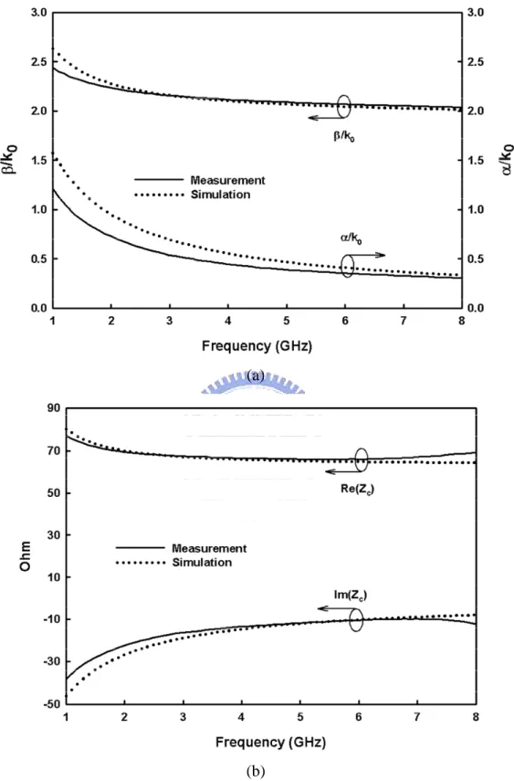
M2 (b)Fig. 2.1 CMOS monolithic 0.18 µm complementary conducting strip transmission line (CCS TL). (a) Straight and bend CCS unit cells. (b) Photograph of the 7.956 mm meandered CCS TL test structure with W equal to S. The right inset illustrates the material parameters.
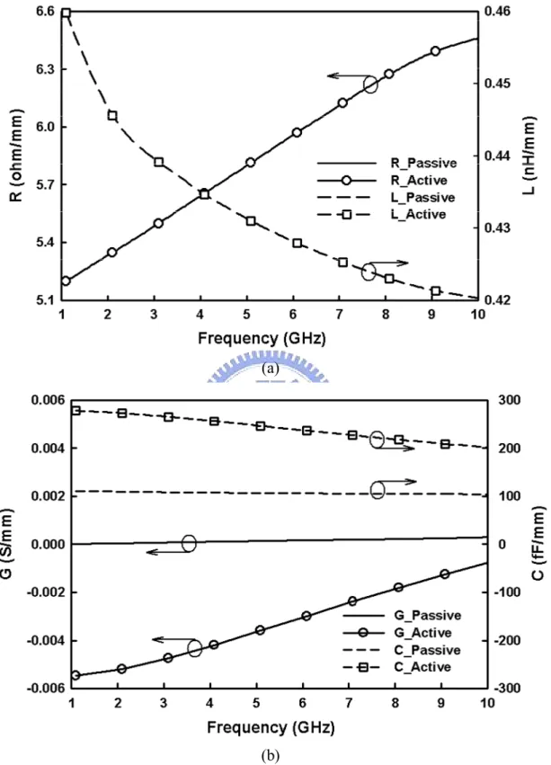
The data derived form the measurement and simulation are show in solid and dotted lines in Fig. 2.2. For clearness, the complex propagation characteristics (γ=α+jβ) were illustrated as the normalized phase constant (β/k0) and attenuation constant (α/k0),
respectively. Through the entire spectrum, the simulated propagation constants were in good agreement with the measured data, as shown in part (a) of Fig. 2.2. The maximum deviation of the normalized phase constant is 0.17 at 1.0 GHz and less than 0.03 from 4 to 8 GHz. Regarding the normalized attenuation constant, the maximum deviation is 0.34 at 1 GHz and continuously get smaller as frequency increased. For example, at 6 and 8 GHz the deviations are reduced to 0.05 and 0.02. Within the C-Band spectrum, from 4 to 8 GHz, the root-mean-square (RMS) values of the normalized phase constants derived from the measurement and simulation are 2.04 and 2.07. The corresponding values of the normalized attenuation constants are 0.36 and 0.42. Part (b) of Fig. 2.2 plots the real (Re(Zc)) and imaginary (Im(Zc)) parts of
complex characteristics impedance (Zc). The RMS values of real part characteristic
impedances derived from the measurement and simulation are 64.86 and 66.78 Ω. The corresponding values of imaginary parts are 10.57 and 11.04 Ω, respectively. In summary, the relative RMS deviations of γ and Zc are 2.65% and 2.99% across the
C-Band. The data shown in Fig 2.2, therefore, have demonstrated the software-based analysis method could predict the guiding characteristics of meandered CCS TLs in CMOS 0.18µm technology with a reasonable confidence level, a deviation less than 3 percentages.
(a)
(b)
Fig. 2.2 Measurement and simulation results of equivalent transmission line characteristics of the meandered 0.18 µm CMOS CCS TL in Fig 2.2(b) from 1 to 8 GHz. (a) Normalized attenuation (α/k0) and phase (β/k0) constants. (b) Real (Re(Zc))
2.2 Comparative Study of CCS TL against Microstrip in Meandered
Configuration
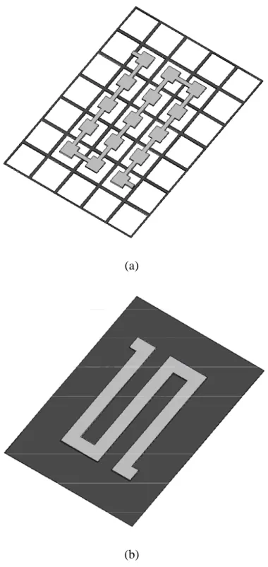
Many observations of meandered CCS TLs against microstrips (MS) in printed circuit board (PCB) technology had been reported in [28, 32]. The comparative study performed in this section, rather, emphasized on CMOS monolithic technology for compact microwave integrated circuit integration and guiding properties of meandered CCS TLs with high characteristic impedances (Zc). The particular 0.18 µm
CMOS technology applied to this study was identical to that of the validity-check experiment in Section 2.1. In order to have enough impact on guiding properties of meandered CCS TLs, the ground plane opening and the periodicity were enlarged to 40 µm and 44 µm. The width of central patch was varied from 2 µm to 30 µm corresponding to the minimum and maximum permissible width of Metal-6 layer. In additional to the meandered CCS TL cases of equal connecting arm and central patch, the cases of S unequal to W with S = 6 µm and S = 15 µm are also included. Part (a) of Fig. 2.3 indicates a 5 x 3 2D meandered CCS TL of S = 6 µm and W = 20 µm. For a fair comparison, the meandered layout pattern of the microstip is arranged the same as that of the meandered CCS TL, as demonstrated in Fig. 2.3(b). The line width of the microstrip is also set equal to the center patch (W) of the CCS TL. The software-based analysis method is applied to derive the guiding properties, real part of Zc (Re(Zc)), normalized phase constant (SWF), and loss per guiding wave length
(dB/λg), of meandered CCS TLs and microstrips at 6.0 GHz. The analyzed results are
(a)
(b)
Fig. 2.3 Meandered test structures used at the comparative study of CCS TL anagist microstrip in standard CMOS 0.18 µm technology. (a) 5 x 3 2D meandered CCS TLs with W, S, Wh, and P equal to 20, 6, 40 and 44 µm. (b) Meandered microstrip with a
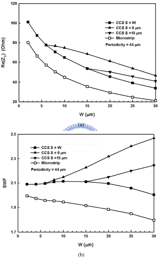
When W is 2, 10 and 30 µm, the real part of characteristic impedance (Re(Zc)) of
the meandered CCS TL of S equal to W, plotted in the solid black square symbol in Fig. 2.4(a), illustrates a 20.95, 19.89, and 12.57 ohm increase of the corresponding meandered microstrips (MS), drawn in the hollow square one. This result shows that the meandered CCS TL of S equal to W possesses a higher characteristic impedance than that of the meandered MS. Compared the meandered CCS TLs of S unequal to W with S equal to W, the increase in Re(Zc) is average 12.32 and 6.12 ohm when S = 6
µm and S = 15 µm for W varying from 20 µm to 30 µm. As expected, a wider S would results in a wider MS section within the meandered CCS TL introducing a lower value of Zc [28]. Nevertheless, the meandered CCS TL with non equal S and W
is a more efficient guiding structure for designing high characteristic impedance and suitable for compact layout integration. Regarding the sensitivity on variations in W, the Zc for meandered CCS TL of S = 6 µm decreased 8.26 ohm when W increased from 8 µm to 15 µm and decreased 6.12 for S = 15 µm and W increased from 20 µm to 30 µm. However, the decreases of Zc for the meandered microstrip against the same
variations in W were 20.0 and 8.04 ohm, respectively. These observations indicate that the meandered CCS TL with non equal W and S is less sensitive in lowering Zc due to the meanderings than the meandered microstrip.
Part (b) of Fig. 2.4 plotted the slow wave factors (SWF) of meandered CCS TLs and microstrips against W. As could be observed easily, the SWFs of the meandered CCS TLs of S equal to W are almost insensitive to the change of W across the entire range of interest. The averaged SWF of the particular case is 2.085 with a maximum deviation of only 1.37%. Since a wider S or an equivalent wider MS section would cause a decrease in the effective series inductive component. But a wider W would also results an increase in the effective shut capacitive component (C). Therefore, the
resultant phase constant, proportional to LC , has insignificant changes. However the effective Zc, proportional to
(
R+jωL) (
G+jωC)
, would be lowered which hadbeen observed in Part (a) of Fig. 2.4. Moreover, the meandered CCS TLs of S unequal to W show even slower guiding properties than S equal to W. Since their effective series inductive component (L) were not changed due to a fixed size of S. But the effective shunt capacitive part (C) were enlarged with the increase of W. Thus the resultant SWFs exhibit monotonically increases against W. On the contrary, SWFs of the meandered microstrips fall from 1.995 to 1.797 with a decrease rate of 9.9% when W increase from 2 µm to 30 µm. Therefore the meanderings of microstips cause a significant reduction in the SWF. Which reflecting the fact the propagating characteristics of meandering CCS TLs are less susceptible to the meanderings than the meandered microstrips.
Figure 2.5 depicts the loss per guiding wavelength (dB/λg) against Re(Zc). The size
of W employed in each structure was also shown beneath the corresponding symbol in the same figure. When Re(Zc) above 61.24 Ω, the meandered CCS TLs of S unequal
to W with S = 6 µm demonstrate lower loss properties than that of the meandered TLs of S equal to W. Since the average metal strip of the first structure is averagely wider than the second one. Besides the first structure also has a shorter guiding wavelength, inversely proportional to the SWF, as explained before. Therefore a better loss characteristic for high-impedance CCS TL of S unequal to W in meandered form could be expected. Compared to meandered microstrips, either meandered CCS TLs of S unequal to W or S equal to W demonstrates lower dB/λg at the same
high-characteristic-impedance region. The behind mechanism also relies on a wider metal strip and superior slow wave property. When Re(Zc) is about 80 ohm, for
TLs of S equal to W and S unequal to W are 30.89% and 44.74%, respectively. For characteristic-impedance below 57.23 ohm, the meandered microstrip has the lowest loss property, but the corresponding SWF and Re(Zc) are much sensitive to
the meanderings, as discussed previously. Base on an equal W, however, meandered CCS TLs of S unequal to W demonstrates not only higher Re(Zc), better SWF and
lower dB/λg than those of meandered CCS TLs of S equal to W. The validity of these
facts could be justified through comparing the performance among the first structure of S = 15 µm and the S equal to W cases when W varied from 20 to 30 µm. Following observations could be summarized according to Fig. 2.4 and 2.5: the averaged increase ratios on Zc and SWF are 16.03% and 7.13%, and reduction ratio on dB/λg is
4.29%, respectively. The mechanism by which the dB/λg decrease by reducing S
mainly involves an increase in the effective series inductive component, since the attenuation constant could be approximately expressed asR C L when the effective shunt conductive component is negligible. Besides, the first structure also has a superior SWF property. It is evident that meandered CCS TL of S unequal to W has more advantages than the ones of S equal to W in terms of guiding properties.
(a)
(b)
Fig. 2.4 Transmission line characteristics of meander CCS TL and meandered microstip derived from the software-based analysis method at 6.0 GHz. (a) Real part of characteristic impedance (Re(Zc)), and (b) slow wave factor (SWF).
Fig. 2.5 Loss per guiding wavelength (dB/λg) of meandered CCS TL and meandered
2.3 Discussion
In this chapter the guiding characteristics of CMOS 0.18 µm monolithic meandered CCS TL with non equal and equal connecting arm (S) and central patch (W) have been analyzed. The meandered CCS TL compared to the meandered microstrip has at least three advantageous points: (1) less sensitive to lowering characteristic impedance and slow wave factor by meanderings, (2) better loss characteristics for high-impedance lines, (3) higher characteristic impedance value for wide metal strip. Of more interest is the fact that the meandered CCS TL with non equal S and W even shows a better transmission line performance than the one with equal S and W on the same advantageous points.
CHAPTER 3
Approaches of Microwave Active Filters
This chapter investigates an innovating approach of fully monolithic CMOS active filters incorporating meandered complementary-conducting-strips transmission line aimed for filtering functions commonly required by the radio receiver front end. Conventionally these functions are performed by off-chip SAW filters. Recently, on-chip BAW filters had also been proposed to overcome this impediment with an additional payment of process modifications. However, by introducing integrated active elements compensating or emulating the on-chip passive components, active filters exhibiting good frequency selectivity, low passband attenuation, and small in size show considerable interest. Section 3.1 gives a general overview of active inductor and active resonator techniques traditionally employed in active filter deisgns. Then a preliminary experiment of a 5 GHz active bandpass filter based on active CCS transmission lines is introduced in Section 3.2.
3.1 Overview on Active Inductor and Active Resonator Techniques
Analog LC-Ladder filter, in 1966, had been discovered to be highly insensitive to component variation [33]. In integrated circuit (IC) technology, planar or stacked spiral inductors are usually applied for implementing large inductances. However, several fundamental problems such as excess series resistance, high-frequency resonances, and mutual coupling limit its usefulness. Therefore, active inductors have been developed to replace the passive ones.
Since the gyrator network has an impedance inversion property. An active gyrator with a capacitive load, therefore, could simulate an active inductor and be
used in realizing inductorless active filters [34]. Monolithic active gyrators could also be constructed with op-amp or transconductor circuits [35]. Overlap capacitance between the input and output of the monolithic CMOS transconductor, however, normally introduces phase lag in the transconductance function and limits the maximum usable frequency of this active inductor [36]. Canceling of this overlap capacitance by a balanced gyrator topology had been successfully applied in the VHF (up to several hundreds of MHz) active filter design [37]. For the use of active gyrator in monolithic microwave integrated circuit, several active notch filter designs had been reported in GaAs technoloy [38-40].
Using a common-source cascode-FET with resistive feedback topology to implement a relatively lossy broadband monolithic GaAs active inductor had been report in [41]. A significant reduction in the series resistance of this active inductor with the use of common-gate cascode-FET feedback arrangement was lately published in [42]. To realize a broadband flat inductive response, however, either configuration requires the two Cgs capacitances of each FETs must be identical to
cancel each other out. The required transconductance (gm) of each FET must larger
than (ωCgs)1.5, and the maximum operating frequency of this active inductor is ideally
about one-half of the small-signal unity frequency (ft= gm/2πCgs) of the FET. The
related applications in monolithic GsAs tunable narrow-band active filters were reported in [43-46].
As a well-known approach, the negative resistance (-R) circuit could be used to compensate the loss in passive transmission line, lump inductor, or lump capacitor to realize an active filters. For an active LC resonator, the –R circuit is an integral part of the lumped LC resonator to cancel out the dissipative loss. This technique had been used in monolithic CMOS, SiGe, and GaAs technologies [7-8, 19-24, 47-54]. For
spiral inductor usually has a lower resonance frequency and could not provide a broadband flat inductive response. Thus a Q factor tuning circuit has to be adopted within the filtering system [18, 23-24]. In contrary, transmission line is a distributed element and demonstrates a broader and much stable characteristic against frequency. Therefore monolithic CCS TL is applicable for active filter designs for its advantageous guiding property and less sensitive to meandering as discussed in Chapter 2. The remaining challenge is how to compensate its propagating loss in the CMOS monolithic approach. To date, several design techniques had been developed to integrate the negative resistance circuit with distributed transmission lines in hybrid and GaAs technologies [55-58]. For example, C. Y. Chang et al. had used coupled line resonators and coupled negative resistance to realize a hybrid tunable 200-MHz wide active bandpass filter at 10.5 GHz [55]. M. Ito at al. had implemented a monolithic 2.6-GHz wide active bandpass filter at 65 GHz by applying two CPW transmission line quarter-wave resonators terminated by negative resistances in GaAs technology [56]. To get a clear insight in the restrictions and feasibilities of the negative resistance circuits used both in active LC and transmission-line resonator, some negative resistance circuits commonly appeared in the literature would be surveyed in the following subsection.
Apart from the techniques mentioned above, some bandpass or notch amplifiers have been built by cascading a passive bandpass or notch segment with the low noise amplifier (LNA) [10, 59-61]. However, these filter have restricted frequency selectivity and not applicable for the general filter synthesis methods. Nevertheless, this approach is advantageous for its compactness and design simplicity. In contract, the transverse or recursive typed active bandpass filter usually requires 3-dB coupler, power combiner, and LNAs to perform analog signal processing [62-67]. The general filter synthesis methods could neither be applied to this filter.
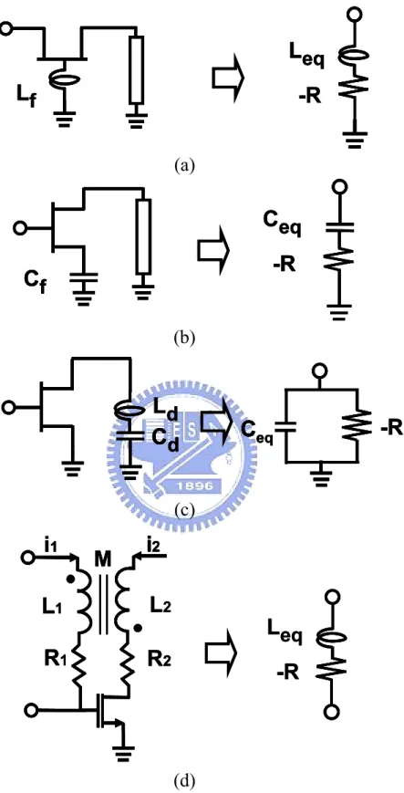
3.1.1 Negative Resistance Circuits
In the circuit topologies requiring single active device, the circuit can be in common gate configuration with an inductive feedback, in common-source configuration with a capacitive feedback, or in common-source and common-drain inductive and capacitive series feedback, as shown in Fig. 3.1(a), (b) and (c). In the ideal case, the negative resistance circuit of Fig. 3.1(a) has an input impedance at the source terminal given by
gs m gs f 2 in C j g C L 1 Z ω + ω − = (1)
This circuitry is fist introduced in [68] and also called the active inductor. By considering the gate resistance and other parasitics of a real transistor, this circuit could not achieve negative resistance without introducing an additional inductance in the drain terminal. Another drawback is the requirement of large Lfresulted from the
high frequency phase shift introduced by the transconductance of a real device [53, 69]. For the ideal case of Fig. 3.1(b), the input impedance at the gate terminal is expressed as ¸ ¸ ¹ · ¨ ¨ © § ω + ω − ω − = f gs f gs 2 m in C 1 C 1 j C C g Z (2)
As can be observed, the higher frequency the more transconductance or power consumption is required to generative an equivalent negative resistance. Besides, the Cgs capacitance from the real device has a negative impact on the resulting negative resistance. Which could set inherent limitations for its usefulness in CMOS technology. The negative resistance circuit shown in Part (c) of Fig. 3.1 is also called the active capacitor. This circuit has demonstrated a superior noise performance in hybrid topology [70]. However, the bandwidth of negative resistance usually involves
a tradeoff between the value of Ld and parasitic resistance within the series feedback network at the drain terminal [71]. Which may enhance the design complexities and increase iteration times.
Part (d) of Fig.3.1 illustrates the coupled-inductor negative resistance circuit. The ideal effective input impedance seen at the primary inductor could be expressed as
) ( R 1 1 2 1 1 1+ ω + ω = + ω + ω θ = j in R j L j M Ae i i M j L j Z (3)
where Aejθ is the current ratio between the primary and secondary inductor, and M is the mutual inductance between the two inductors. When θ equals to 900 or 2700, a negative resistance is generated and could be used to cancel the series resistance R1 of the primary inductor L1. This technique has been applied in CMOS technology for several active bandpass filters design [7, 19]. Notably, the capacitive coupling between the two inductors could cause phase difference in Aejθ and additional capacitive loss. Besides, CMOS on-chip transformer also suffers from the substrate loss [7]. In other words, this negative resistance circuit also has to compromise with the parasitic effects of on-chip inductive lump components.
In contrast, the small-signal resistance at the drain terminal of a Λ-type MOSFET, as illustrated in Fig. 3.2 (a), is inherently negative requiring no inductive component. Since under proper biasing conditions, the slop of its source-drain current (IDS) is inversely proportional to the increase of the source-drain voltage (VDS). The detailed physics of this voltage-controlled single-ended negative resistance device had been reported in [72]. For high frequency applications the bandwidth and tuning capability of a Λ-type MOSFET realized in a typical 0.18 µm CMOS technology is further investigated through circuit simulation. The transistor size (width/length) of N1, N2
and N2 NMOS are 0.5/0.18, 0.35/0.18, and 1.88/0.18 µm, and the VD potential of the Λ-type MOSFET is set at 1.05 volt. For clearness, the output impedance was transformed to equivalent shunt elements, as shown in Fig. 3.2(b). Both the magnitudes of negative conductance (-G) and intrinsic capacitance (C) were proportional to the DC potential at the gate terminal (VG). The total power consumptions were 163.5 and 520.2 µW when VG is 1.4 and 1.8 volts, respectively. Besides, the negative conductance worked at least up to 10 GHz. Thus a Λ-type MOSFET has demonstrate its advantageous features in terms of requiring no passive component, low power, and low complexity and applicable to loss compensation in 0.18 µm CMOS technology.
L
f
-R
L
eq
L
f
L
f
-R
L
eq
-R
L
eq
(a)
C
f
-R
C
eq
C
f
C
f
-R
C
eq
-R
C
eq
(b)
C
d
L
d
-R
C
eqC
d
L
d
C
d
L
d
-R
C
eq-R
C
eq(c)
L
2R
2L
1R
1i
1i
2M
-R
L
eq
L
2R
2L
1R
1i
1i
2M
L
2R
2L
1R
1i
1i
2M
L
1R
1i
1i
2M
-R
L
eq
(d)
Fig. 3.1 Several circuit topologies of negative resistance circuit. (a) common-gate inductive feedback. (b) common-source capacitive feedback. (c) common-source and common-drain inductive and capacitive series feedback. (d) Coupled-inductor negative resistance generator.
-G
V
DC
V
DV
GN
1N
2N
3-G
V
DC
V
DV
GN
1N
2N
3 (a) (b)Fig 3.2 (a) The Λ-type MOSFET and its equivalent small signal circuit. (b) The input susceptance (Y=-G+jωC) of a typical 0.18 µm Λ-type MOSFET when VD biased at 1.05 volt and VG biased at 1.8 and 1.4 volt. The geometrical size (width/length) of N1, N2 and N2 NMOS transistors are 0.5/0.18, 0.35/0.18, and 1.88/0.18 µm, respectively.
3.2 CMOS Active CCS Transmission Line
To compensate the loss in a passive transmission line via negative resistance circuit, conventional approach is by using the negative resistance at the desired frequency band as introduced in Section 3.1. This section will explore the innovating approach of changing the transmission line characteristics fundamentally. At high frequency, as already known, the signal wavelength is comparable to the physical dimension of a transmission line. Thus one could utilize a negative resistance device to amplify the voltage and current along the lossy transmission line within periodic distance much smaller than the guided wavelength. Therefore the complete guiding structure is active in nature. The concept is illustrated in Fig. 3.3(a). The original per-unit-length shut conductance component within the distributed transmission line model is replaced by negative conductance. By using Λ-type MOSFETs as the negative resistance device, the complete schematic including biasing voltages and a passive transmission line is shown in Fig. 3.3(b). The DC potential VD of all Λ-type MOSFETs is carried at the signal trace of the original passive transmission line. The negative resistance tuning mechanism of Λ-type MOSFET is used to adjust the gain of this active transmission line by set the DC potential of VG.
The guided wavelengths of the particular CMOS meandered CCS TL analyzed in Section 2.1 range from 34.72 to 18.20 mm when frequency varies from 4 to 8 GHz. Using an negative resistance to distributed compensate the loss within this TL, therefore, the negative resistance device should be inserted along the TL in a periodic distance much smaller than the guided wavelength at the highest frequency. For the first active CCS TL design, the Λ-type MOSFET was attached in every 3 CCS unit cells, a periodic distance of 102 µm, approximately five-thousandths of the guided wavelength of the passive CCS TL at 8 GHz.
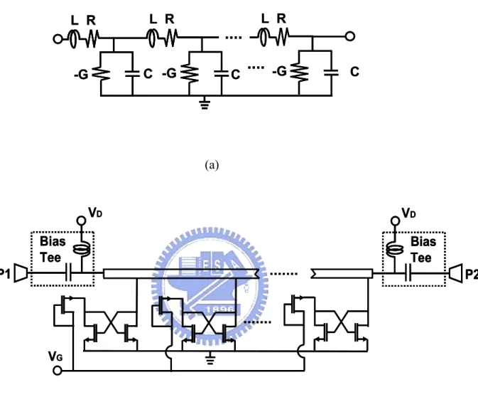
-G -G -G L R L R L R C -G C -G C -G L R L R L R C C C (a) VD VD VG Bias Tee P2 Bias Tee P1 VD VD VG Bias Tee P2 Bias Tee P2 Bias Tee P1 Bias Tee P1 (b)
Fig 3.3 (a) The distributed transmission line model of the proposed active transmission line circuit. (b) The schematic of the proposed active transmission line adopting Λ-type MOSFETs.
The validity of this concept is checked by the same complex propagating characteristics and characteristic impedance extraction procedure from two-port scattering parameters described in Section 2.1. For clearness, the inductance (L), capacitance (C), resistance (R), and conductance (G) per unit length (mm) of the passive and active CCS transmission lines are illustrated in part (a) and (b) of Fig. 3.4. As expected, the series impedance (Z=R+jωL) per unit length of the transmission lines had not been changed, but the shunt susceptance (Y=G+jωL) element had been affected after the Λ-type MOSFETs are inserted. The sign of the unit-length conductance had been changed from positive to negative and the unit-length capacitance had also been increased. These observations match to the proposed concept of active transmission line. Apart from the lossless transmission line whose characteristic impedance is real and equal to L C, the unit-length resistance and conductance of this active transmission line could not be neglect after attaching the negative resistance device. As shown in Fig. 3.5(a), the resultant characteristic impedance still possesses an imaginary part, and the magnitude is dropped due to the increase of unit-length conductance and capacitance. Regarding propagating characteristics, illustrated in part (b) of Fig. 3.5, the slow wave factor was increased from 2.09 to 3.28 and the gain per guiding wavelength increased from -8.5 to 0.025 dB/λg around 5.5 GHz. The active transmission line now has gain from 1 to 6 GHz. Thus, this distributed loss compensation approach applied in monolithic CMOS technology had been theoretically validated and could be further applied to the active filter design.
(a)
(b)
Fig. 3.4 The extracted distributed transmission line parameters of passive and active CCS TLs from 1 to 10 GHz. (a) Series resistance and inductance per millimeter. (b) Shunt conductance and capacitance per millimeter.
(a)
(b)
Fig. 3.5 The guiding characteristics of passive and active CCS TLs from 1 to 10 GHz. (a) Characteristic impedances (Zc). (b) Gain per guiding wavelength (dB/λg) and slow wave factors (β/k0).
3.3 A 5.5 GHz Active Bandpass Filter
Conventional transmission line based active bandpass filters either use passively coupled active resonators [55-58]. This section investigates the actively coupled active resonators approach based on the architecture of the so-called dual-behavior resonator (DBR) transmission line bandpass filter [32]. The active transmission lines presented in Section 3.2 are applied to realize the required DBRs and impedance inverters (J inverters) within the active bandpass filter.
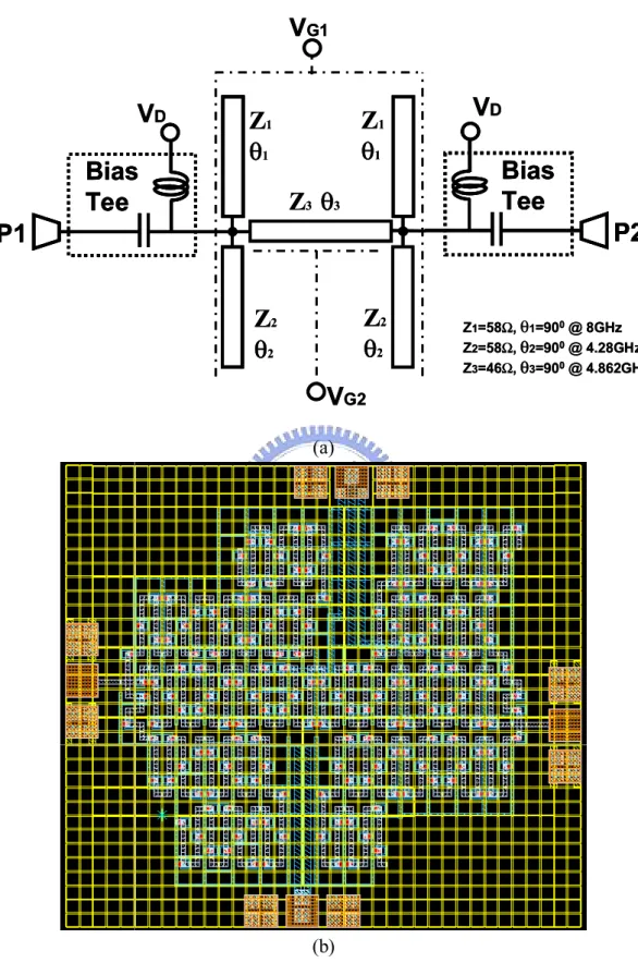
The ideal equivalent circuit of a second-order 5.5 GHz DBR active transmission line (TL) bandpass filer is illustrated in Fig. 3.6(a). Each DBR is realized by one 900 active transmission line with Re(Zc) equal to 58 ohm at 8 GHz and another at 4.28 GHz. The series J inverter is realized by one 900 active transmission line with Re(Zc) equal to 46 ohm at 4.862 GHz. The size of periodicity, mesh ground plan, central path, and connecting arms for the CCS unit cell employed by all the CCS TLs are 34µm, 30µm, 6µm, and 6 µm, respectively. The Λ-type MOSFETs with the transistor size reported in Section 2.2.1 were attached to the CCS TL in every three CCS unit cells. Regarding the N3 NMOS transistor used at the Λ-type MOSFET for the J inverter is 1.5 µm larger than those used at two DBRs to achieve the desired Re(Zc). For simplicity, the DC potential required by drain terminals of Λ-type MOSFETs are all set to 1.0 volt and biased through the two ports of the prototype filter. The VG1 and VG2 voltages are 1.8 and 1.45 volt, respectively. The chip area is 1.19 x 1.19 mm2 including right and left-side ground-signal-ground pads for the two ports of the prototype filter and up and lower-side ones for VG1 and VG2.
Z
3θ
3Z
1θ
1Z
2θ
2Z
1θ
1Z
2θ
2V
DV
DV
G1V
G2 Z1=58Ω,θ1=900@ 8GHz Z2=58Ω,θ2=900@ 4.28GHz Z3=46Ω,θ3=900@ 4.862GHzBias
Tee
P2
Bias
Tee
P1
Z
3θ
3Z
1θ
1Z
2θ
2Z
1θ
1Z
2θ
2V
DV
DV
G1V
G2 Z1=58Ω,θ1=900@ 8GHz Z2=58Ω,θ2=900@ 4.28GHz Z3=46Ω,θ3=900@ 4.862GHzBias
Tee
P2
Bias
Tee
P2
Bias
Tee
P1
Bias
Tee
P1
(a) (b)Fig. 3.6 (a) The schematic of the 5.5 GHz active bandpass filter based on the active CCS TLs. (b) The layout diagram of the 5.5 GHz active bandpass filter.
Figure 3.7(a) plots the simulated two-port scattering parameters based on 50 Ω reference impedance from 1 to 10 GHz. Two reflection zeros can be observed at 4.5 and 5.7 GHz. The central frequency is 5.5 GHz with a 3-dB bandwidth from 4.5 to 6.2 GHz and the simulated passband gain is 1.6 dB from 5.0 to 6.0 GHz. The return loss is below 9.0 dB from 4.3 to 5.7 GHz with an out-band rejection below 30 dB from 8 and 20 dB at 3.3 GHz. The total power consumption of this prototype active filter is about 35.70mW and the simulated input referred noise figure at the central frequency is 15.37 dB. However, the reflection coefficient is above zero dB from 1 to 1.8 GHz and from 6 to 8 GHz. Examining the real part of susceptance from the input of the prototype active filter, as illustrated in Fig. 3.7(b), an extremely large negative conductance is observed below 1 GHz. Further lowering the tuning voltages, VG1 and VG2, could not totally remove the negative conductance from the input of the active filter unless the Λ-type MOSFET introduces no negative resistance anymore. Since the particular device generate more negative resistance at lower frequencies than at high-frequency band. Lowering VG does not change this trend against frequency but result in an overall decrease in the generated negative resistance and consequently deteriorating the filtering characteristics of the active CCS TL based filer.
After powering on the fabricated prototype active filter and performing on-wafer scattering parameter measurements with Agilent 8510C VNA, the measured results, as shown in Fig 3.8 (a), are not a filter responses but tremendous reflecting signals from the active filter. The measured input frequency spectrum from DC to 1 GHz is also shown in part (b) of Fig 3.8. The strongest oscillating signal is observed at 10.1 MHz with a power level of -8.3 dBm. Examining the inset of Fig 3.7 (b), one could easily recognize that the most negative input conductance of the active filter is -46 mS at 40 MHz. This frequency shift is caused by the parasitic within the measurement
(a)
(b)
Fig. 3.7 The small signal characteristics of the 5.5 GHz second-order DBR bandpass filter based on active CCS TLs incorporating Λ-type MOSFETs. (a) Two-port scattering parameters from 1 to 10 GHz. (b). Real part on input susceptance (Re(Yin)) at P1 from DC to 10 GHz.
(a)
m1
freq=
TraceA=-8.333
10.10MHz
m1
freq=
TraceA=-8.333
10.10MHz
0.2 0.4 0.6 0.8 0.0 1.0 -100 -80 -60 -40 -20 -120 0 freq, GHz TraceAm1
dB mm1
freq=
TraceA=-8.333
10.10MHz
m1
freq=
TraceA=-8.333
10.10MHz
0.2 0.4 0.6 0.8 0.0 1.0 -100 -80 -60 -40 -20 -120 0 freq, GHz TraceAm1
dB m (b)Fig. 3.8 Measured results of the 5.5 GHz second-order active bandpass filter. (a) Small-signal scattering parameter from 1 to 10 GHz. (b) The frequency spectrum at P1 from DC to 1 GHz.
3.4 Discussion
In this chapter several microwave active filter techniques employing the active inductor and the active resonator have been reviewed. Conventionally these techniques rely on the active transistor with low intrinsic capacitance (Cgs), high quality inductively feedback network, good transconductance efficiency, or good matching properties. To make monolithic CMOS active filters without these restrictions, an active CCS TL based approach had been chosen for its favorable lossless guiding characteristics and low complexity so that general filter synthesis methods could be used. However, the preliminary experiment was failed for instability issues at 10.1 MHz. Therefore the design philosophy must apply adequate loss compensation in order to make the active filter stable through the entire frequency spectrum. This strategy will be explored in Chapter 4 in view of the filter’s architecture.
CHAPTER 4
Miniaturized C-Band Active Bandpass Filter
This chapter presents a C-Band monolithic active bandpass filter based on Q-enhanced half-wavelength resonators in a standard CMOS 0.18 µm technology. The quality factor of the complementary-conducting-strips transmission line (CCS TL) based half-wavelength resonator is reported in Section 4.1. Section 4.2 describes the design philosophy of the composite Q-enhanced resonator incorporating the cross-coupled pair circuit with the CCS-TLs based half-wavelength resonator. Within this novel architecture, the loss-composition mechanism could be well controlled both in architecture level and circuitry level. The two operation modes of the Q-enhanced resonator are theoretically investigated. Section 4.3 presents the realization of the second-order prototype bandpas filter based on the proposed Q-enhanced resonator in great detail. When consumes 3.0 mA from a 1.8 V supply, the active filter demonstrates a 2.2-dB insertion loss. Theoretically analyzed two-port scattering parameters are in good agreements with the measured results. The trend of the active bandpass filter with a 0.56-dB transmission gain is also theoretical and experimentally investigated. For this particular case, however, the reflection coefficient is greater than 0 dB from 6.5 GHz to 7.9 GHz. Based on a set of 50-Ω terminations, the noise and nonlinear properties of the prototype filter with a 2.2-dB insertion loss are further analyzed in Section 4.4 and 4.5. The stability analysis of the proposed active filter is performed in Section 4.6. Section 4.7 compares the filter performance with other published works and indicates the direction for further improvements.
4.1 CCS TL Half-Wavelength Resonator
In view of miniaturizing the size of complementary-conducting-strips transmission line (CCS TL) based half-wavelength resonator, the meandered CCS TL of the largest slow wave factor (SWF) should be employed. But there will be both DC and microwave signals carried in the top layer strip of the meandered CCS TL. Therefore the one with equal W and S of 30 µm is the best candidate for lowering the power dissipation introduced by the DC resistance. Base on the studies performed in Section 2.2, one can quickly estimate the physical length of a half-wavelength resonator by using CCS unit cells of W = S = 30 µm, P = 44.0 µm, and Wh= 40 µm at 6.0 GHz to be 12,480 µm and such meandered transmission line can be compacted in an chip area of 748 x 748 µm2. In contract, if the similar meandered microstip of a 30-µm width is applied, there will be an additional length requirement of 1.42 mm corresponding to a 12.1 % increase in the chip area. Though the loss property of meander microstrip is about 1.5 dB lower than the meandered CCS TL for a half-wavelength resonator at 6.0 GHz. But it would be clearer in Section 4.2 that this impediment could be easily overcome by applying negative resistance circuit.
However, for example, the meandered CCS TL of W=30 µm and S = 15 µm posses a better loss characteristic, better slow property, and modest average width in the top layer strip compared to the one of W = S = 30 µm. With the CCS TL of unequal W and S, a passive half-wavelength resonator could be further optimized in respect to the DC-resistance, high-frequency loss, and chip area. But for simplicity and for the same reason about the loss issue, the meandered CCS TL of S = W = 30 µm is employed for designing the prototype active bandpass filter.
For clearness, the guiding characteristics of CCS TL of S = W = 30 µm from 1 GHz to 8 GHz is derived by using the same software-based analysis method described in Chapter 2. Figure 4.1 illustrates the extracted results of the particular CCS-TL design example. From 1.0 GHz to 8.0 GHz, the real part of the characteristics impedance (Zc), which is the solid line plotted in Fig. 4.1(a), nearly keeps at a constant value of 34.2 Ω. The imaginary part of Zc is capacitive, ranging from -11.7 Ω to -2.04 Ω. The normalized phase constant shown in solid line in Fig. 4.1(b) illustrates the value of 2.0 at the desired operating frequency. The normalized attenuation constant, which is plotted by the dotted symbol in Fig. 4.1(b), however, shows relatively high loss aspect of the transmission line. In the low frequency limit (1 GHz), the metal thickness employed in the CCS-TL is smaller than the skin depth, thus we observe larger attenuation losses. Figure 4.2 plots the Q-factor of CCS-TL against frequency, showing 2.19, 2.94, and 3.40 at 3.0GHz, 5.0GHz, and 6.53GHz, respectively. Therefore the Q-factors our resonator design are comparable but smaller than those of inductor-based design in [18-20, 22-24].
(a)
(b)
Fig. 4.1 Guiding characteristics of the meandered CMOS CCS TL with W = S = 30 µm, P = 44 µm, and Wh = 40 µm from 1 to 8 GHz. (a) Complex characteristic impedance. (b) Normalized complex propagation constant.
Fig. 4.2 The Q-factor of the CCS TL-based half-wavelength resonator from 1 to 8 GHz.
4.2 Q-Enhanced Monolithic Half-Wavelength Resonator
Figure 4.3 illustrated the concept of a Q-enhanced complementary-conducting- strips (CCS) half-wavelength resonator. A cross-coupled pair, which consists of two identical NMOS transistors, is integrated into a passive CCS-TL based half-wavelength resonator. The Drain terminal of N1 is directly connected to the Gate terminal of N2 and vise versa. Two transistors are biased at the same DC potential (VG), and the Drain terminals of both N1 and N2 are directly loaded with CCS half-wavelength resonator, forming a new composite resonator.
CCS
λ
g/2
Resonator
A
B
N1
N2
V
GV
GCCS
λ
g/2
Resonator
A
B
N1
N2
V
GV
GFig. 4.3 Q-enhanced CCS half-wavelength resonator incorporating a NMOS cross-coupled pair.