Dependence of luminescence efficiency on dopant concentration and sintering
temperature in the erbium-doped Ba 0.7 Sr 0.3 TiO 3 thin films
Shou-Yi Kuo, Chin-Sheng Chen, Tseung-Yuen Tseng, S.-C. Chang, and Wen-Feng Hsieh
Citation: Journal of Applied Physics 92, 1868 (2002); doi: 10.1063/1.1492870
View online: http://dx.doi.org/10.1063/1.1492870
View Table of Contents: http://scitation.aip.org/content/aip/journal/jap/92/4?ver=pdfcov Published by the AIP Publishing
Articles you may be interested in
Phase separation and direct magnetocaloric effect in La 0.5 Ca 0.5 MnO 3 manganite J. Appl. Phys. 113, 123904 (2013); 10.1063/1.4794179
Magnetoresistive properties of p - La 0.78 Mn 0.99 O 3.5 and p - La 0.80 Mn 1.04 O 3.5 nanocomposites at temperatures 4.2 – 300 K and magnetic fields to 140 kOe
Low Temp. Phys. 34, 757 (2008); 10.1063/1.2973716
Modeling the crystal-field splitting of energy levels of Er 3 + ( 4 f 11 ) in charge-compensated sites of K Pb 2 Cl 5 J. Appl. Phys. 100, 043108 (2006); 10.1063/1.2244416
Evidence of electronic phase separation in Er 3+ -doped La 0.8 Sr 0.2 MnO 3 Appl. Phys. Lett. 82, 2865 (2003); 10.1063/1.1570001
Electrical characterization of the p- Hg 1x Zn x Te interface after anodic sulfidization treatments J. Vac. Sci. Technol. A 16, 2300 (1998); 10.1116/1.581344
Dependence of luminescence efficiency on dopant concentration and
sintering temperature in the erbium-doped Ba
0.7Sr
0.3TiO
3thin films
Shou-Yi Kuo
Institute of Electro-Optical Engineering, National Chiao Tung University, 1001 Ta-Hsueh Road, Hsinchu, Taiwan 30050, Republic of China
Chin-Sheng Chen and Tseung-Yuen Tseng
Department of Electronics Engineering and Institute of Electronics, National Chiao Tung University, 1001 Ta-Hsueh Road, Hsinchu, Taiwan 30050, Republic of China
S.-C. Chang and Wen-Feng Hsieha)
Institute of Electro-Optical Engineering, National Chiao Tung University, 1001 Ta-Hsueh Road, Hsinchu, Taiwan 30050, Republic of China
共Received 22 February 2002; accepted for publication 20 May 2002兲
We found the dependence of luminescence efficiency on Er3⫹ concentration and sintering temperature in the Er-doped Ba0.7Sr0.3TiO3共BST兲 thin films is governed by crystallinity and ion–ion
interaction. X-ray diffraction and Raman studies of the sol-gel prepared samples show that the BST polycrystalline phase occurred when the sintering temperature reaches 700 °C, whereas, it becomes worse for temperature above 700 °C resulting from phase separation and the Er3⫹ concentration exceeding 3 mol % due to charge compensation mechanism. The observed green emission reaches maximum at sintering temperature 700 °C and 3 mol % Er3⫹ions concentration. We also showed the Er dopant does not affect the dielectric property of BST thin films in C–V measurement and the Ba0.7Sr0.3TiO3films doped with Er3⫹ions may have potential use for electroluminescence devices.
© 2002 American Institute of Physics. 关DOI: 10.1063/1.1492870兴
I. INTRODUCTION
Study on the luminescent properties of rare-earth 共RE兲-doped materials is strongly motivated because of their tech-nological applications in photonic devices and next-generation flat-panel displays. Rare-earth ions exhibit a characteristic intra-4f shell luminescence which is nearly both host material and temperature independent. This feature can be used to tune the emission spectra for specific appli-cations. Thus, it is important for systematic research of the RE ions doped in different kinds of host materials with good mechanical, thermal, electrical and electro-optical properties. Recently, many Er3⫹-doped materials have been extensively studied because of the blue 共2H9/2→4I15/2兲, green 共4S
3/2,2H11/2→4I15/2兲 and red 共4F9/2→4I15/2兲 upconversion
emissions and the laser actions having been realized in a variety of glasses and fluoride crystals.1– 4 In comparison with the previously mentioned materials, barium strontium titanate is a dielectric material with excellent dielectric prop-erties such as high dielectric constant, small dielectric loss, low leakage current, and large dielectric breakdown strength. Therefore, it is a good candidate for a RE doped host mate-rial.
Thin films of the high dielectric material Ba0.7Sr0.3TiO3 共BST兲 have been intensively studied in recent years of
appli-cations in high density dynamic random access memories
共DRAMs兲, monolithic microwave integrated circuit used for
decoupling capacitors, tunable microwave filters, and phased
array antennas.5–17 The high dielectric constant of BST of-fers the potential of producing denser memories with simpler capacitor structures than those fabricated with conventional silicon dioxide or silicon nitride dielectrics. Combining with the merits of electricity, BST:Er will be a promising candi-date for optoelectronic devices.
BST thin films have been fabricated using various meth-ods, including metalorganic chemical vapor deposition
共MOCVD兲,18 rf sputtering,19 thermal evaporation,20 MBE,21
and laser ablation.22Among those, sputtering and laser abla-tion are the most widely used. However, there are still some difficulties in using these processes to fabricate homoge-neous films on large substrates 共more than 50 mm in diam-eter兲. Due to the variation in composition and thickness the quality of films is often degraded. In contrast, the sol-gel process has the advantage of large area deposition, in addi-tion to its low cost and convenience process control.23
In this article, we report the effect of Er concentration with sintering temperature on photoluminescence共PL兲 prop-erties in sol-gel derived Er-doped Ba0.7Sr0.3TiO3 共BST:Er兲
thin films and discuss the mechanism of emission quenching.
II. EXPERIMENT
The starting materials used for sol-gel processes were barium acetate, strontium acetate, titanium isopropoxide, and erbium acetate. Acetic acid and ethylene glycol were used as solvents. Formamide was selected as an additive to adjust the solution viscosity in order to reduce the cracks of BST thin films. Ba(CH3COO)2and Sr(CH3COO)2with molar ratio of
7:3 and proper amount of erbium acetate were fits dissolved
a兲Author to whom correspondence should be addressed; electronic mail: [email protected]
1868
0021-8979/2002/92(4)/1868/5/$19.00 © 2002 American Institute of Physics [This article is copyrighted as indicated in the article. Reuse of AIP content is subject to the terms at: http://scitation.aip.org/termsconditions. Downloaded to ] IP:
in heated glacial acetic acid. After these starting materials were completely dissolved in heated glacial acetic acid, eth-ylene glycol was added into the solution and a condensation reaction occurred. Then a stoichiometric amount of Ti-isopropoxide was added into solution. Finally, formamide was added to adjust the viscosity of BST:Er precursor solu-tion. The BST:Er precursor solution was clear and transpar-ent.
The BST:Er precursor solution was spin coated on the Pt/TiO2/SiO2/Si substrates and silicon substrates at 3000
rev./min for 30 s. After each spin coating, the samples were heated at 200 °C for 10 min to dry the gel and then pyrolyzed at 500 °C for 30 min in furnace. A suitable heating rate was used to avoid cracking of the BST films. Thicker films can be obtained by repeating the spin-coating process. Finally the samples were sintered at different temperature. All the sin-tered samples were studied by x-ray diffraction, Raman, and photoluminescence spectroscopy.
X-ray diffraction patterns共XRD兲 were carried out to ex-amine the structure of the films by using a Siemens D5005 diffractometer 共Cu target with a working voltage of 40 kV and current of 40 mA兲 in a scanning rate of 4°/min. For photoluminescence共PL兲 and Raman measurements, the 488 nm line of an Ar⫹ laser was used as the excitation source. The emission was then analyzed using a SPEX 1877C triple grating spectrograph equipped with a cooled CCD at 140 °K. A Pt top electrode was deposited by rf sputtering for a metal/ insulator/metal 共MIM兲 structure to perform the C–V mea-surement. Capacitance–voltage analyses were performed at a frequency of 100 kHz using an HP8142 impedance analyzer.
III. RESULTS AND DISCUSSION
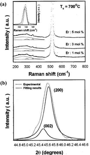
The crystalline nature of the films was identified by x-ray diffraction共XRD兲. Figure 1共a兲 shows the XRD patterns of 200-m-thick two-layer films on Pt/TiO2/SiO2/Si at
vari-ous sintering temperatures 600– 800 °C. The BST:Er thin films sintered at 600 °C show weak perovskite phase with
共100兲, 共110兲, and 共200兲 orientations. Meanwhile, the
second-ary phases Er2O3 and (Ba,Sr)2Ti2O5CO3 were also found
from XRD at 35°, 42°, and 27° indicated in Fig. 1共a兲, respectively.24,25As the sintering temperature is increased to 700 °C, the peaks of the XRD patterns become sharper and more intense, indicating better crystallinity and larger grain size. The 700 °C sintered films possess good perovskite crys-tallinity without the existence of second phase and are con-sistent with the previous report.24,25However, when the sin-tering temperature is above 750 °C, the diffraction lines at 27.5° and 29° due to Er2Si2O7 consistent with the JCPDS data were recognized. It is believed that Er2Si2O7phase ap-peared at the interface between BST:Er thin films and silicon substrate during the process of the high temperature sintering.26 In addition, the minor line at 31° that has been ascribed to Er2Ti2O7phase was observed as well.27,28 We
show the XRD patterns of BST films doped with various Er concentrations sintered at 700 °C in Fig. 1共b兲. It indicates that the BST thin film doped with Er 1 mol % has the best crystallinity and the largest grain size共57 nm兲 and the grain size decreases to 28 nm while the Er concentration increases
to 5 mol %. The origin of the worst crystallinity was attrib-uted to the Er3⫹ substitution for Ba2⫹, which will be dis-cussed later.
The Raman spectra of BST:Er films with various Er con-centration sintered at 700 °C are plotted in Fig. 2共a兲. We found a broad band centered at 260 cm⫺1 corresponds to A1(TO2) phonon mode, the 300 cm⫺1 peak is attributed to
the B1 and E共TO⫹LO兲 modes, and the asymmetric broad
band near 520 cm⫺1 corresponds to E共TO兲 and A1(TO3) modes.29A comparison of these Raman modes with various Er doping shows the increase of FWHM for the higher Er concentration. It indicates the higher Er concentration is the worse crystallinity, which is consistent with the XRD results. The appearance of sharp Raman peak at 300 cm⫺1is a sig-nature of the tetragonal phase BaxSr1⫺xTiO3 polycrystalline
as described in Ref. 30. This specific Raman mode becomes broadened and weakened while phase transition from the te-tragonal to cubic occurs. It is known that one can control the Curie temperature TCof bulk BaxSr1⫺xTiO3by adjusting the
ratio of Ba/共Ba⫹Sr兲 by an approximate relation: TC(K)
⫽360x⫹40,31of which a structural change from
centrosym-metric cubic to noncentrosymcentrosym-metric tetragonal phase at room FIG. 1. XRD patterns of BST:Er thin films sintered at various temperatures
共a兲 and doped with various Er concentrations at sintering temperature
700 °C共b兲.
1869
J. Appl. Phys., Vol. 92, No. 4, 15 August 2002 Kuoet al.
temperature when x⬃0.75. Because it has been reported that the Curie temperature of BaTiO3 film is much higher than
the bulk,32 our Ba0.7Sr0.3TiO3 films should belong to the
te-tragonal rather than the cubic phase that is confirmed by the expanded XRD data around 45.5° shown in Fig. 2共b兲.
The 3 mol % Er ions doped BST thin films sintered at 600, 700, and 800 °C show dielectric constants共⑀兲 of around 230, 320, and 440 as shown in Fig. 3. The dielectric constant raised with increasing sintering temperature which is consis-tent with the previous report.33Hence, the addition of the Er dopant in this range did not affect the dielectric constant, characteristics of a good capacitor for BST.
The mechanism of emission of Er3⫹-contained materials
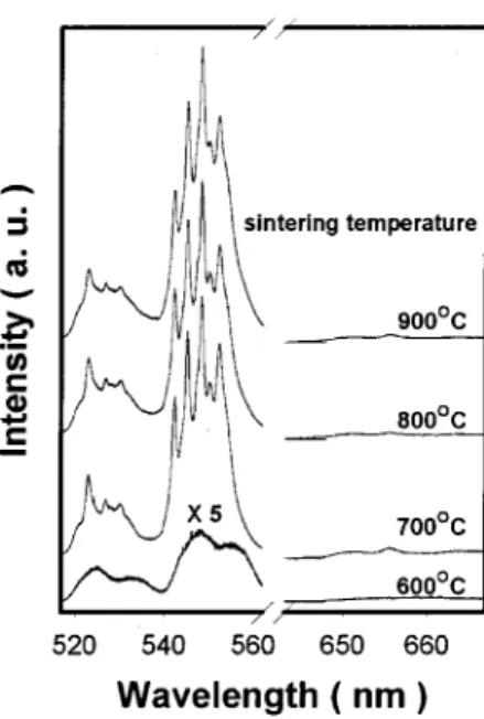
has been well established in the literature34,35and the energy diagram is schematically shown in Fig. 4. The PL spectra of Ba0.7Sr0.3TiO3 films doped with 3 mol % of Er are shown in
Fig. 5 for sintering temperatures at 600, 700, 800, and 900 °C under the 488-nm-laser excitation at room temperature. Since the host material has tetragonal rather than cubic struc-ture, the transition selection rules of the Er ions are relaxed and the Er-related emission can be observed. The green peaks at 530 and 550 nm are attributed to the Er3⫹ inner shell 4f 2H11/2 and 4S3/2 to the 15I15/2 ground level,
respec-tively, and the weak red emission centered at 600 nm is ascribed to the4F
9/2→15I15/2.
Obviously, the shapes of the PL spectra seem quite dif-ferent for the films sintered at various temperatures. There are only few broad peaks in the main emission wavelength for the film sintered at 600 °C. On the other hand, the peaks become sharper and split into several fine peaks when the films are sintered above 750 °C. The characteristic emission peaks in these films were attributed to the Stark splitting of the degenerate 4f levels under the crystalline field, and ho-mogeneous and inhoho-mogeneous broadening caused by the film’s texture structures and multidomain structures. This is consistent with the XRD analysis in which the samples sin-tered at 600 °C indicated amorphous or weak perovskite phase and polycrystalline phase while increasing the sinter-ing temperature.
In order to compare the relationship between the green emission and the crystallinity, shown in Fig. 6 are the PL intensities of 600, 700, 800, and 900 °C. For all the Er dop-ing, the green emission at 550 nm reaches its maximum at FIG. 2. Raman spectra of BST thin films doped with various Er
concentra-tions at sintering temperature 700 °C 共a兲 and typical expanded XRD data around 45.5°共b兲. The dotted and solid lines represent the experimental and fitting results, respectively.
FIG. 3. ⑀–E plot of the BST:Er film capacitors sintered at 600, 700, and 800 °C.
FIG. 4. Relevant energy levels in the PL of BST:Er thin films: excitation laser photon wavelength共488 nm兲 and Er3⫹4f energy levels.
700 °C and is partially quenched when the samples are sin-tered at temperature above and below 700 °C. The diversity of emission behavior related to Er3⫹ concentration of thin films sintered at various temperatures is apparent. The quenching of the green emission which occurred in the BST:Er films is directly related to microstructural changes caused by the crystallinity, which will be discussed in detail. From the XRD data as shown in Fig. 1共a兲, we have con-cluded that only weak crystalline phases were found in the films sintered at 600 °C and the crystallization occurred at 700 °C but formation of Er2Si2O7 and Er2Ti2O7phases form
above this temperature. Now, we concentrate on the influ-ence of sintering temperature upon emission intensities. When the films belong to the weak crystalline phase sintered at 600 °C, the luminescence efficiency is low due to high defect density. The green emission reaches maximum at sin-tering temperature 700 °C indicates that the improvement of
the crystallinity will enhance the luminescence efficiency, whereas the emission intensities decrease while the sintering temperature is above 700 °C. The quenching of the emission intensity may arise from the formation of other phases. Not only the complex compounds, e.g., Er2O3, (Ba,Sr)2Ti2O5CO3, Er2Si2O7, and Er2Si2O7suppress the
lu-minescence efficiency due to optical scattering or absorption, but the Er2O3has cubic symmetry as well. While the Er ions occupy the centrosymmetry position of Er2O3 crystal, the 4S
3/2→4I15/2 transition is forbidden and therefore would
re-duce luminescence efficiency.
For studying the effect of Er3⫹ concentration on emis-sion intensity of the BST:Er films, we found as shown in Fig. 6 the emission intensities increase with increasing Er3⫹ con-centration for 600 °C sintered BST:Er films which have the weak crystalline phase. The doped Er3⫹ ions in the weak crystalline phase are dissolvable. A noticeable difference contrast to the films in weak crystalline phase was observed while the BST:Er thin films belong to polycrystalline phase, sintered at 700, 800, and 900 °C. It can be clearly seen that the emission intensities of the BST:Er films increase as the Er doping concentration increases from 1 to 3 mol %. Mean-while, the PL intensity diminishes as Er doping concentration exceed 3 mol %.
The quenching mechanism is thought to be a cross-relaxation process between two closely placed Er3⫹ ions. In this experiment, the ion density N of 1, 3, and 5 mol % Er doping is 1.5⫻1020, 4.5⫻1020, and 7.5⫻1020/cm3, respec-tively. Ion pairs and clusters can be formed easily in the Ba0.7Sr0.3TiO3 lattice.36,37The Er3⫹ ion is likely to take the
position of the Ba2⫹or Sr2⫹due to similar ionic radius. The substitution of Er3⫹ for the nearest Ti4⫹ ion in the oxygen octahedron is difficult because of large difference in size between Er3⫹and Ti4⫹. To maintain electrical neutrality, one approach is to replace the nearest Ba2⫹ion by another Er3⫹
ion with, additionally, the formation of a Ba vacancy. As shown in Figs. 1共b兲 and 2共a兲, the increase of Er3⫹ concen-tration from 1 to 5 mol % results in the worse crystallinity. From charge compensation mechanism, the smallest Er3⫹
⫺Er3⫹distance is about 0.4 –0.5 nm in Ba
0.7Sr0.3TiO3lattice
and cross relaxation is greatly enhanced, resulting in de-crease in luminescence intensity. Very efficient cross relax-ation can occur when two or more Er ions sit close to one another to form a cluster that results in almost immediate interaction between the ions.38 The interaction strength is very sensitive to the change in ␥, which is the distance be-tween two Er3⫹ions, and is found to be proportional to 1/␥m
共m⫽6, 8, and 10兲.2
In our Ba0.7Sr0.3TiO3 thin films doped
with 1, 3, and 5 mol % Er, the mean distance between Er3⫹ ions is estimated by ␥⫽0.62⫻N⫺1/3,39 corresponding to ␥
⫽1.2, 0.81, and 0.68 nm. It is very likely the mean distance
of 0.68 nm of 5 mol % BST:Er will increase the probability of Er3⫹ ions sitting at the nearest-neighbor positions. Not only slightly structural damage was found from XRD and Raman measurement, but also enhanced luminescence quenching was observed. Consequently, the emission inten-sity diminishes while the Er concentration exceed 3 mol %. FIG. 5. Room temperature photoluminescence spectra from BST thin films
doped with 3 mol % of Er under various sintering temperatures.
FIG. 6. Dependence of the green emission intensities of BST:Er thin films on Er concentration and sintering temperature.
1871
J. Appl. Phys., Vol. 92, No. 4, 15 August 2002 Kuoet al.
IV. CONCLUSION
The BST:Er films prepared by sol-gel technique under various sintering temperatures have been studied by XRD,
C–V, Raman, and PL measurements. We found that the
BST:Er films belong to weak crystalline phase sintered at 600 °C and polycrystalline phase sintered above 700 °C. The addition of Er dopant does not downgrade the electronic property of barium–strontimum titanate. The emission effi-ciency of BST:Er thin films was found to be dominated by the mean distance between Er3⫹ ions and solubility of Er3⫹ in polycrystalline and weak crystalline phase. The emission intensities of the films reach maximum at 3 mol % Er ions dopant concentration and sintering temperature 700 °C. The presence of clusters for the Er concentration exceed 3 mol % will diminishes the emission intensity. Moreover, the im-provement of the crystallinity of BST:Er films enhances the green emission enhancement. Good performance on both electric and optical properties of the BST:Er thin films show potential applications in photonic devices.
1J. Heikenfeld, M. Garter, D. S. Lee, R. Birkhahn, and A. J. Steckl, Appl. Phys. Lett. 75, 1189共1999兲.
2
H. X. Zhang, C. H. Kam, Y. Zhou, X. Q. Han, S. Buddhudu, Q. Xiang, Y. L. Lam, and Y. C. Chan, Appl. Phys. Lett. 77, 609共2000兲.
3S. M. Takahashi, M. Kanno, and R. Kawamoto, Appl. Phys. Lett. 65, 1874
共1994兲.
4J. Heikenfeld, D. S. Lee, M. Garter, R. Birkhahn, and A. J. Steckl, Appl. Phys. Lett. 76, 1365共2000兲.
5R. Liedtke, M. Grossmann, and R. Waser, Appl. Phys. Lett. 77, 2045
共2000兲.
6N. A. Pertsev, V. G. Koukhar, R. Waser, and S. Hoffmann, Appl. Phys. Lett. 77, 2596共2000兲.
7
J. Im, S. K. Streiffer, O. Auciello, and A. R. Krauss, Appl. Phys. Lett. 77, 2593共2000兲.
8S. M. Rhim, H. Bak, S. Hong, and O. K. Kim, J. Am. Ceram. Soc. 83, 3009共2000兲.
9
A. I. Kingon, J. P. Maria, and S. K. Streiffer, Nature共London兲 406, 1032
共2000兲.
10D. E. Kotecki, J. D. Baniecki, H. Shen, R. B. Laibowitz, K. L. Saenger, J. J. Lian, T. M. Shaw, S. D. Athavale, C. Cabral, P. R. Duncombe, M. Gutsche, G. Kunkel, Y. J. Park, Y. Y. Wang, and R. Wise, IBM J. Res. Dev.
43, 367共1999兲.
11J. D. Baniecki, R. B. Laibowitz, T. M. Shaw, K. L. Saenger, P. R. Dun-combe, C. Cabral, D. E. Kotecki, H. Shen, J. Lian, and Q. Y. Ma, J. Eur. Ceram. Soc. 19, 1457共1999兲.
12
C. S. Hwang, B. T. Lee, C. S. Kang, K. H. Lee, H. J. Cho, H. Hideki, W. D. Kim, S. I. Lee, and M. Y. Lee, J. Appl. Phys. 85, 287共1999兲.
13J. D. Baniecki, R. B. Laibowitz, T. M. Shaw, P. R. Duncombe, D. A. Neumayer, D. E. Kotecki, H. Shen, and Q. Y. Ma, Appl. Phys. Lett. 72, 498共1998兲.
14G. W. Dietz, M. Schumacher, R. Waser, S. K. Streiffer, C. Basceri, and A. I. Kingon, J. Appl. Phys. 82, 2359共1997兲.
15C. Basceri, S. K. Streiffer, A. I. Kingon, and R. Waser, J. Appl. Phys. 82, 2497共1997兲.
16G. T. Stauf, C. Ragaglia, J. F. Roeder, D. Vestyck, J. P. Maria, T. Aygua-vives, A. Kingon, A. Mortazawi, and A. Tombak, Integr. Ferroelectr. 39, 1271共2001兲.
17
S. C. Tidrow, E. Adler, T. Anthony, W. Wiebach, and J. Synowczynski, Integr. Ferroelectr. 29, 151共2000兲.
18
B. S. Kwak, K. Zhang, E. P. Boyd, A. Erbil, and B. J. Wilkens, J. Appl. Phys. 69, 767共1991兲.
19
S. Kim, S. Hishita, Y. M. Kang, and S. Baik, J. Appl. Phys. 78, 5604
共1995兲.
20
K. Iijima, T. Terashima, K. Yamamoto, K. Hirata, and Y. Bando, Appl. Phys. Lett. 56, 527共1990兲.
21
R. A. McKee, F. J. Walker, J. R. Conner, E. D. Specht, and D. E. Zelmon, Appl. Phys. Lett. 59, 782共1991兲.
22
K. Nashimoto, D. K. Fork, F. A. Ponce, and J. C. Tramontana, Jpn. J. Appl. Phys., Part 1 32, 4099共1993兲.
23
F. Wang, A. Uusimaki, S. Leppavuori, S. F. Karmanenko, A. I. Dedyk, V. I. Sakharov, and I. T. Serenkov, J. Mater. Res. 13, 1243共1998兲. 24C. L. Jia, K. Urban, S. Hoffmann, and R. Waser, J. Mater. Res. 13, 2206
共1998兲.
25
S. Hoffmann and R. Waser, J. Eur. Ceram. Soc. 19, 1339共1999兲. 26K. Hafidi, Y. Ijdiyaou, M. Azizan, E. L. Ameziane, A. Outzourhit, T. A.
Nguyen Tan, and M. Brunel, Appl. Surf. Sci. 108, 251共1997兲. 27
J. H. Hwang, S. K. Choi, and Y. H. Han, Jpn. J. Appl. Phys., Part 1 40, 4952共2001兲.
28J. H. Hwang and Y. H. Han, Jpn. J. Appl. Phys., Part 1 40, 676共2001兲. 29
M. DiDomenico, S. H. Wemple, and S. P. Porto, Phys. Rev. 174, 524
共1968兲.
30R. Naik, J. J. Nazarko, C. S. Flattery, U. D. Venkateswaran, V. M. Naik, M. S. Mohammed, G. W. Auner, J. V. Mantese, N. W. Schubring, A. L. Micheli, and A. B. Catalan, Phys. Rev. B 61, 11 367共2000兲.
31
S. Y. Kuo, W. Y. Liao, and W. F. Hsieh, Phys. Rev. B 64, 224103共2001兲. 32C. L. Li, Z. H. Chen, Y. L. Zhou, H. B. Lu, C. Dong, F. Wu, and H. Chen,
J. Appl. Phys. 86, 4555共1999兲. 33
S. Ezhilvalavan and T. Y. Tseng, Mater. Chem. Phys. 65, 227共2000兲. 34C. H. Huang and L. McCaughan, IEEE Photonics Technol. Lett. 9, 599
共1997兲.
35
K. W. Kramer, H. U. Gudel, and R. N. Schwartz, Phys. Rev. B 56, 13 830
共1997兲.
36
F. Goutaland, Y. Ouerdane, A. Boukenter, and G. Monnom, J. Alloys Compd. 275-277, 276共1998兲.
37J. Zheng, Y. Lu, X. Chen, M. C. Golomb, and J. Zhao, Appl. Phys. Lett.
75, 3470共1999兲.
38W. J. Minscalco, J. Lightwave Technol. 9, 234共1991兲.
39C. Y. Chen, R. R. Petrin, D. C. Yeh, W. A. Sibley, and J. L. Adam, Opt. Lett. 14, 432共1989兲.