i
國 立 交 通 大 學
電信工程研究所
碩 士 論 文
針對開放式線段缺陷的診斷性自動測試向量產生器與其診斷流程設計
Diagnostic ATPG for Open-Segment Defects and Its Diagnosis Flow
研究生:陳彥后
指導教授:溫宏斌
ii
針對開放式線段缺陷的診斷性自動測試向量產生器與其診斷流程設計
學生:
陳彥后指導教授
:溫宏斌國立交通大學電信工程研究所碩士班
摘
要
當電路發生開放式線段缺陷,實體電路上的缺陷周圍的其他邏輯閘造成的偶
和電容及拜占庭效應對缺陷影響到的輸出會隨著缺陷的位置改變,許多先前的研
究針對開放式缺陷的測試和檢驗。這篇論文提供了一個利用兩個階段產生診斷性
測試向量的方法:首先使用布林可滿足性引擎在單一缺陷的假設下,針對發生缺
陷影響到的邏輯閘自動產生向量。另外搭配上兩階段的診斷方法,分別使用一個
修正的字典(dictionary)診斷法,去減少可能發生錯誤開放式缺陷的候選線段數
量,接著在利用注入和評估(inject-and-evaluate)診斷法使得結果能夠達到很高的
準確性。實驗執行在 ISCAS85 的電路上,結果顯示在檢測方面最後的解析度(即
對應的候選線段數量)可以達到幾乎接近 1 的準確性。
。
ii
Diagnostic ATPG for Open-Segment Defects and Its Diagnosis Flow
student:
Yan-Hou ChenAdvisors:Dr. Hung-Ping Wen
Institute of Communication Engineering
National Chiao Tung University
ABSTRACT
As an open defect occurs on one segment in the circuit, the coupling
capacitances from the neighboring nets and the Byzantine effect based on
the physical layout and cell library can result in different faulty behaviors.
Many previous researches focus on the test and diagnosis issue for open
defects. However, the diagnosability of test patterns is not well addressed.
Therefore, in this paper, we propose a high-resolution algorithm which
consists of two stages: (1) a diagnostic ATPG and (2) its diagnosis flow.
A Boolean Satisfiability solver is incorporated to generate patterns for
target driven gates of the open segment under the single defect
assumption. Later, the diagnosis flow first constructs the set of candidates
based on a dictionary-based approach followed by an inject-and-evaluate
analysis with the assistance of physical information to greatly reduce the
candidate size. Experiments are conducted on ISCAS85 benchmark
circuits and the results show that the proposed algorithm runs efficiently
and can deduce nearly 1 candidate for each individual open-segment
defect.
iii
誌
謝
論文以完成,首先要感謝是這幾年來溫宏斌老師的細心教導,從老師身上學 到許許多多的事情,他也和我們分享知識上以及生活上的一切。在我對研究徬徨 無助的時候,給予適時的協助,引領我的方向,指證我的錯誤。一路走來即使困 難重重,卻因為有老師,才會如此甘之如飴,能成為老師的學生覺得相當慶幸, 他所作的一切,對我的影響,良師益友說來相當貼切。未來職場和由研究的領域 上,我會更加努力,不辜負老師的期望。 另外,還要感謝 CIA LAB 的同仁,張佳玲學姐、高振源學長、廖千慧、陳韋 廷、郭雨欣、張家慶、吳欣恬,因為有你們實驗室也有了歡樂的學習環境,更加 有活力。可以和你們在學習和研究上互相切磋,相信我都成長了不少。 最後,將此論文謹獻給我的父母、家人和曾經幫助過我的人。
iv
Contents
LIST OF FIGURES ... V LIST OF TABLES ... VII
INTRODUCTION... 1
PREVIOUS WORKS... 6
FAULT MODEL OF OPEN SEGMENTS ... 10
DIAGNOSTIC AUTOMATION TEST PATTERN GENERATION(ATPG) FLOW ... 12
DIAGNOSIS FLOW ... 26
EXPERIMENTAL RESULTS ... 32
CONCLUSION ... 39
v
List of Figures
FIG. 1.1 SEM PHOTO OF METAL TUNNEL OPEN ... 2
FIG. 1.2 (A) OPEN CRACK IN A METAL LINE AND (B) ITS ELECTRICAL EQUIVALENT: A CAPACITOR VOLTAGE DIVIDER ... 3
FIG. 1.3 (A) TUNNELING OPEN AND (B) RESPONSE TO ELECTRON TUNNELING ... 3
FIG. 1.4 (A) LOGIC LEVEL (B) BYZANTINE EFFECT ... 4
FIG. 3.1 FAULT MODEL FOR AN OPEN DEFECT ... 11
FIG. 4.2(B) EXAMPLE OF COP ... 17
FIG. 4.4 EXAMPLE ABOUT AFFECTS OUTPUTS ... 18
FIG. 4.5(A) SORT THE COUPLING CAPACITANCES ... 19
FIG. 4.5(B) BUILD THE BRANCH AND BOUND TREE ... 20
FIG. 4.5(C) SATIFY THE THRESHOLD VOLTAGE ... 20
FIG. 4.5(D) CHANGE OTHER NETS COMBINATIONS ... 21
FIG. 4.5(E) LOGIC CONFLICT IN CHOOSING LOGIC VALUE ... 21
FIG. 4.5(F) ABORTED FAULT ... 22
FIG. 4.5(G) CHECK THE FAULT ACTIVATION ... 23
FIG. 4.5(H)CHECK THE FAULT PROPAGATION ... 24
vi
FIG. 4.5(J) EXAMPLE OF CHECK ROBUSTNESS ... 25
FIG. 5.1 DIAGNOSIS FLOW ... 27
FIG. 5.2 DIVIDE DIAGNOSIS FLOW INTO TWO STAGES... 28
FIG. 5.3(A) DEFECT OCCUR IN S2 ... 28
FIG. 5.3(B) PATTERN, P2 AND ITS OUTPUT RESULT O2 ... 28
FIG. 5.3(C) PATTERN, P3 AND ITS OUTPUT RESULT O3 ... 29
FIG. 5.3(D) PATTERN, P4 AND ITS RESULTS ... 29
FIG. 5.3(E) BACKTRACE TO THE DEFECT ... 30
FIG. 5.4 INJECT-AND-EVALUATE METHODS ... 31
FIG. 6.1 DIAGNOSIS FLOW FOR RANDOM PATTERNS AND 5-DETECTION PATTERNS ... 36
vii
List of Tables
TABLE 1 BASIC GATE TABLE ... 15
TABLE 2 ADVANCED GATE TABLE ... 16
TABLE 3 CIRCUIT INFORMATION... 33
TABLE 4 COMPARE WITH OTHER ATPG ... 34
TABLE 5 FAULT CLASSIFICATION ... 34
TABLE 6 DIAGNOSIS RESULTS ... 35
TABLE 7 RANDOM PATTERNS AND 5-DETECTION PATTERN FAULT DICTIONARY ... 37
TABLE 8 5-DETECTION PATTERNS DIAGNOSIS RESULT ... 38
1
Chapter 1
Introduction
2
Open defects can be mainly classified into two kinds of faults: (1) open-segment defects, also known as interconnect open defects, which indicate that unintended breaks or electrical discontinuities in IC interconnect lines occurring in metal, poly-silicon, or diffusion regions; (2) intra-gate opens, regarded as an open with an infinite resistance that disconnects the charge path or discharge path to the gate output, and it is also regarded as stuck-open faults. This paper mainly targets the former.
When open segment defects occur in the circuit, there are many problems. One is the
tunneling effect, which is caused by narrow cracks appearing in metal lines or in a contact or
via. Fig 1.1[1] shows such a defect. The crack is narrow enough to support quantum mechanical electron tunneling. One of famous tunneling mechanisms is Fowler-Nordheim tunneling. Those tunneling effects depend on the characters of the materials, such as the IC with that defect fails in the high temperatures. Another is the floating node. When the crack is wide enough that electrons can’t through the gap, the logic value of the gate containing the defects depends on the coupling capacitances. Fig 1.2(a) and (b)[1] illustrates that condition. The third one is open delay defect, shown in Fig 1.3[1]. If a small crack with metal material has an interesting temperature property for an IC, the frequency becomes lower and lower when temperature is dropping. This is unusual property for an IC, the defect can be difficult to detect in test. Today’s ATPG for interconnect open defects also suffers from too many neighbors’ combinations. It is hard to assign the logic values effectively and quickly. This problem makes open-segment ATPG time-consuming.
3
Fig. 1.2 (a) open crack in a metal line and (b) its electrical equivalent: a capacitor voltage divider [1]
Fig. 1.3 (a) Tunneling open and (b) response to electron tunneling [1]
When the manufacturing process scales down to the deep sub-micron, the distance between metal lines becomes narrower and the probability of defect occurrences becomes higher. When open-segment defects occur, the number of the coupling capacitances increase. To properly model the defect behaviors, the Byzantine effect needs to be considered with the
4
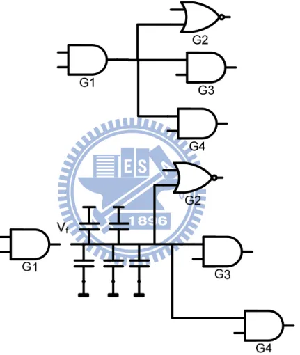
assistance of layout information and the cell library. According to the physical layout, a logical net can be divided into multiple segments as defect sources, not only the net itself[2, 3]. For example, in Fig 1.4(a), gate G1 drives gate G2, G3 and G4 through a logical net. When a defect occurs on the output of G1, all downstream gates, G2, G3 and G4, receive faulty values. However, considering the physical layout shown in Fig. 1.4(b), the net can be further divided into five segments. When an open-segment defect occurs on different segments, the faulty values propagate to different gates and result in different faulty behaviors.
G1
G2
G3
G4
Fig. 1.4 (a) logic level (b) Byzantine effect
For IC diagnosis, two core problems are fault activation and fault propagation. In addition, resolution which denotes the reported number of candidates per fault/defect is also important for the success to diagnosis. For a high-quality diagnosis, both the diagnostic algorithm and patterns needs devising particularly. Therefore, diagnostic test pattern generation (TPG) generates patterns not only with a highly fault coverage but also with different erroneous output syndromes for different defects for diagnosis. As a result, the diagnosis algorithm which ties in diagnostic patterns can reach the high diagnosability and
5
resolution[4]. The state-of-the-art TPG research for open-segment defects focuses on achieving the same fault coverage as stuck-at fault patterns do. When applying these patterns in the traditional diagnosis flow, resolution may not be satisfactory because one error syndrome can be attributed to different defects.
Automatic test pattern generation (ATPG) has been investigated in the test area where many different methods were developed specifically for different faults/defects. ATPG mainly involves three fundamental problems: justification, propagation and implication[5]. The D-algorithm, the first complete ATPG algorithm, relies on analyzing the circuit structure in the early 1960s[6]. The next important landmark is PODEM in 1981[7], which search the primary input assignments with simulation to enhance the computational efficiency. The other approach proposed in 1992 uses Boolean Satisfiability (SAT) based model to represent the logic functionality of a circuit to facilitate pattern generation[8]. In general, SAT-based approaches outperform PODEM-based approaches for most of the cases nowadays.
When a circuit fails after testing, the diagnosis process starts to analyze its behaviors. Basically, diagnosis can be classified into two types: one is cause-effect analysis which mainly uses fault simulation to build a dictionary-based paradigm for each error syndrome[7, 9-11], and the other is effect-cause analysis which focuses on error output to find the candidate as faults/defects in the circuit. As the cause-effect analysis are criticized for unpredicted diagnosis result due to different pattern qualities, most of the recent diagnostic flows belong to the effect-cause analysis and can be further divided into has three categories:
structural pruning[12], backtracing[11, 13], and inject-and-evaluate paradigms[14, 15].
However, effect-cause based diagnostic approaches still suffer from time-inefficiency when tracing error signals from primary outputs towards primary inputs.
Therefore, in this work, we apply a SAT solver to facilitate the diagnostic pattern generation under the assumption of a single defect. Effect of each open-segment defect is further decomposed and reflected on its driven gates, respectively. Moreover, a branch-and-bound algorithm is also used with COP (controllability and observability procedure) to guide the search of solutions. Later, in our diagnostic flow, a hybrid method is proposed and starts from a dictionary-based analysis followed by an inject-and-evaluate analysis. The experimental result shows that the proposed diagnosis can run efficiently and our diagnostic patterns along with the proposed diagnosis flow can achieve a high resolution. For all ISCAS 85 benchmark circuits, nearly only 1 candidate is reported and matches the injected defect.
6
Chapter 2
7
To ensure that no fault exists in the circuit, typically engineers have two ways: one is automatic-test-pattern-generation (ATPG) based approach, and the other is design-for-testability (DFT) based approach. Automatic test pattern generation (ATPG) represents the process of generating effective test patterns for specific problems in a digital circuit efficiently whereas design for testability (DFT) denotes the design techniques that add certain testability features to a circuit design. If the ATPG is powerful to capture all faults, DFT will be useless. For a good ATPG technique, fault equivalence, pattern compaction and pattern compression are the core issues. ATPG can be classified into two types: structure-based ATPG and SAT-based ATPG.
Structure-based ATPG have been investigated for a long time. In 1967, the first algorithm, D algorithm [6], was proposed by Roth and proposed D-frontier and J-frontier during its logic tracing. D-frontier consists of all the gates whose output values are X but have faulty effect values D (or ~D) on their inputs. J-frontier consists of all gates whose output values are known but are not justified by their inputs. When D-frontier and J-frontier collectively derive all values of the circuit, one pattern is found. The next landmark developed in 1981 is Path Oriented Decision Making (PODEM) [7] which only makes decisions at necessary primary inputs. In 1983, the Fanout-Oriented TG algorithm (FAN)[16] proposed by Fujiwara extended the PODEM-based algorithm to remedy these shortcomings.
Until 1992, a new type of methods for ATPG was proposed. In [8], Larrabee showed a method to generate test patterns using Boolean Satisfiability, not backtracing the circuit structure. It combines the correct and faulty circuits into one miter circuit, converts the new circuit into the corresponding conjunctive normal form (CNF), and then uses s SAT solver to find input vectors.
For diagnosing a digital circuit, we usually assume that faults only occur in the combinational part whereas flip-flops and the scan chain are fault-free. Diagnosis algorithms can be divided into two major paradigms: cause-effect analysis and effect-cause analysis [4].
Cause-effect analysis first specifies constraints for the fault type, and then uses fault simulation to build the dictionary as fault lists. Once this dictionary is built, it can be looked up for analyzing the fault syndrome. However, this type of methods mainly suffers from two shortcomings: the dictionary-size problem and the un-modeled fault problem. The former analysis that dictionary should remember all the output responses of each model fault at each clock may exceed the limit of memory size. When the number of test vectors, number of faults and the number of output syndromes are all over 10,000, the dictionary size may go up to 1012 bits [17]. The latter analysis has the fault-escape problem when different types of faults are not built in the dictionary for diagnosis [11].
Effect-Cause analysis directly analyzes the falling patterns and fault syndromes to retrieve the error information. It has several advantages over cause-effect analysis: first, it does not need to depend on a priori fault model; second, it can ne applied to multiple faults;
8
last, it can be adapted to partial-scan designs more easily. The drawback of this solution is the waste of time to explore solutions. This method mainly consists of three sub-categories: structural pruning [12], backtracing[11, 13] and inject-and-evaluate paradigm [14].
Diagnostic resolution depends on not only the diagnosis flow but also the pattern quality. In fact, a pattern set that can achieve a high defect/fault coverage from general ATPG does not necessarily guarantee a high diagnostic resolution and accuracy. Therefore, diagnosis test pattern generation (DTPG) process is needed to facilitate the diagnostic flow. P. Camurati developed a DTPG to generate patterns for the stuck-at fault model in [18] and later Hartanto from [19] targeted sequential circuit in the proposed DTPG.
The open-defect problem has drawn more attentions since the manufacturing technologies scales down to deep submicron. Many researches have addressed the importance of then open-defect problem and proposed solutions for its testing and diagnosis. Previous works for open-segment defects include diagnosis and automatic test pattern generation (ATPG). For ATPG, the core problem is that it involves many constraints from neighboring wires and different threshold voltages of gates from the design library. For diagnosis, the drawbacks of recent diagnosis algorithms are inefficiency and inaccuracy for open defects.
Xue et al showed that ISCAS’85 circuits with high probabilities have different kinds of open defects according to their experimental results [20]. Rodriguez-Montaneze R et al proposed the via also behaves like a wire or an intra-gate component where a open defect may possibly occur, and moreover the number of via may be larger than number of components in the circuits [21]. Needham W. et al also found that open defects can be escaped under the test of stuck-at fault model [22]. Further, Henderson CL et al characterized open defects: it can run correctly in the low frequencies and failed in the high frequencies. This property makes logic testing more difficult[23]. Therefore, researchers start to propose new methods using logic test and current test together. Makki et al showed experimental results to prove that 90.9% to 90.6% faults can be detected by IDDQ tests with transition-fault logic tests[24]. Konuk proposed a method that combines stuck-at fault tests and current based tests to achieve a high coverage as well[25].
More researches even use the logic tests only. S. Spinner built a aggressor -victim model for the inter-layer opens and the intra-layer opens, and generated the patterns automatically[26]. Their experimental results showed a high defected coverage with a small number of patterns. X. Lin et al proposed three methods: static dominant and dynamic dominant and double observation[27]. The former two methods are used to generate patterns while the last one is applied when the output of a gate coincides with one of the neighboring nets of such gate. S. Hillebrecht et al developed a flow that integrates the physical information such as the layout and the cell library[28]. It not only applies the aggressor-victim model for
9
pattern generation but also redefines the untestability for open defects. Their experimental results demonstrate high efficiency. N. Devtaprasanna et al gave a solution of testing intra-gate open defects and reached the complete defect coverage [29]. Roberto G’omez et al used the commercial tool to build a flow from layout extraction to ATPG for interconnect open defect [30].
For open-defect diagnosis, many previous works also take the physical information into account. Huang proposed a diagnosis flow which focuses on single interconnect-defect assumption and uses inject-and-evaluate paradigm for diagnosis, High accuracy was shown[31]. Different views of testing from the gate level down to the physical (segment) level are provided. Zou et al further considered Byzantine effect as well as physical information for their diagnosis of single open defects[3]. Kao et al targeted multiple open-segment defects and proposed a diagnosis flow which uses the falling patterns to formulate constraints for ILP solving and derives the fault combinations automatically[32].
10
Chapter 3
11
Fig. 3.1 Fault model for an open defect
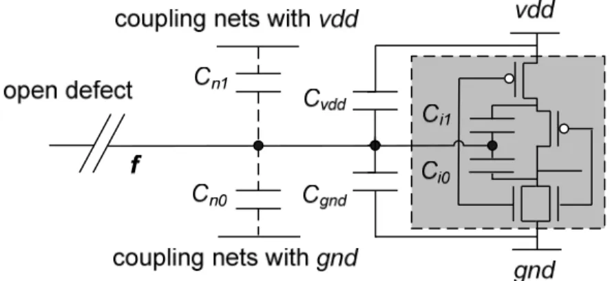
Several fault modes of open defects has already been proposed in previous researches [3, 26, 33]. We use the fault model that describes an open on a segment of net considering the impact of physical information in the paper. When a segment of one net is unintended break, the node f is regarded as an open-segment fault. The voltage of the fault is high-impedance, and the logic value of the floating node f is determined by floating node voltage and threshold voltage of the driven gates. If the floating node voltage is larger than the threshold voltage of a driven gate, the logic value for the driven gate is logic 1. Therefore, the floating nodes do not always become faulty gates.
There is an open segment fault example as Fig. 3.1.the floating node voltage Vf is
counted by the following equation:
gnd t dd f C Q C C C V V + + × = 1 0 1 (3.1)
Where Qt is the initial trapped charge of the floating node and Cgnd is the capacitance
between floating node and ground. C0 and C1 are the sum of the capacitance with logic 1 and
logic 0, respectively. Furthermore, the values of C0 and C1 can be decomposed into: 0 0 0 Cgnd Cn Ci C = + + (3.2) 1 1 1 Cvdd Cn Ci C = + + (3.3)
Where Cvdd and Cgnd are the capacitances between the floating node and the power, and
between the floating and the ground, respectively. Cn0 and Cn1 are the capacitances between
floating node and its neighboring node with logic 0 and logic 1, respectively. Ci0 and Ci1 are
the internal capacitances and reside inside the driven gate. Because Cn0 and Cn1 dominate the
major part of fault behavior, we only observe the coupling effect from Cn0 and Cn1. However,
trapped charge Qt and internal capacitances, Ci0 and Ci1 are typically hard to predict. Process
variation also makes parasitic capacitances extracted from physical layout unpredictable. Therefore, this paper adopts a simplified model similar to [26, 27] by assumption that the parasitic capacitances between the open net and its neighboring nets dominate the decision of the logic value on the following node.
12
Chapter 4
Diagnostic Automation Test Pattern
Generation (ATPG) Flow
13 Benchmark circuit Layout information Coupling capacitance Compute controllability Compute expected floating-net voltage
Decide target logic value Cell
library
Construct and explore the coupling tree
Find one coupling net combination
Satisfiability?
Sat solving of coupling net combination Satisfiability? Check robustness? Matching primary output Primary input assignnment Corresponding faulty gate More combination? Try 5-times abort No Yes No Yes Yes Yes No No More combination? (Pseudo)untestable defects Yes Yes Yes No No Fi Fig. 4.1 Diagnostic ATPG Flow
Having the open segment fault model, the next step focuses on ATPG flow shown as Fig. 4.1 for the generation of diagnostic patterns. A pre-processing step builds an open-segment list for the ATPG. Structurally untestable defects should be removed from the
14
list. Here structurally untestable defects denote those defects with no neighboring aggressor to affect Vf according to the layout and therefore can be dropped from the list.
When an open-segment defect occurs in the circuit, the corresponding voltage value, Vf,
is decided by the logic value of its neighboring combination. Besides a fault can be activated on the segment, a successful ATPG also requires that such fault can propagate and can be observed at one output of the circuits. During the process, fault activation and propagations result in many constraints which collectively make ATPG not easy to solve. The proposed ATPG flow is built upon the assumption of a single open-segment defect and modifies the original stuck-at-fault ATPG with the integration of the physical information.
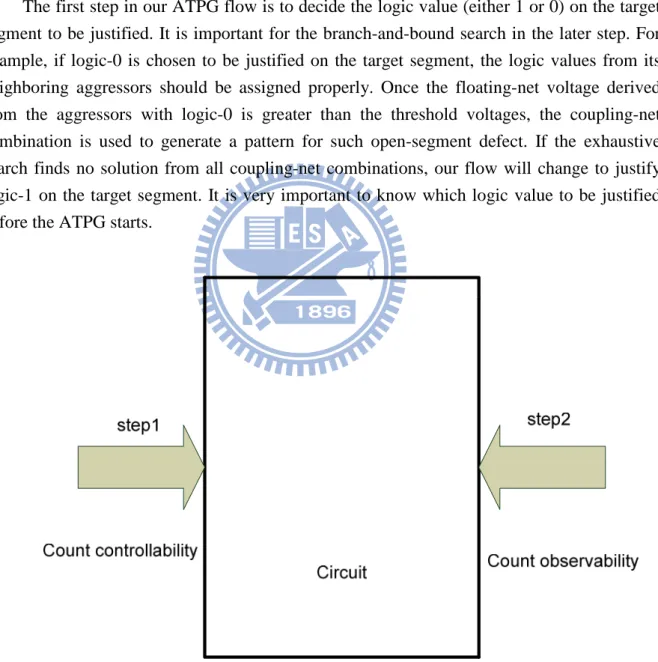
The first step in our ATPG flow is to decide the logic value (either 1 or 0) on the target segment to be justified. It is important for the branch-and-bound search in the later step. For example, if logic-0 is chosen to be justified on the target segment, the logic values from its neighboring aggressors should be assigned properly. Once the floating-net voltage derived from the aggressors with logic-0 is greater than the threshold voltages, the coupling-net combination is used to generate a pattern for such open-segment defect. If the exhaustive search finds no solution from all coupling-net combinations, our flow will change to justify logic-1 on the target segment. It is very important to know which logic value to be justified before the ATPG starts.
Fig. 4.2 (a) controllability and observability procedure COP
There exist multiple metrics such as signal probability and testability to provide information for deciding the logic value of the target segment We choose the controllability
15
and observability procedure (COP) shown as Fig. 4.2, to estimate the most likely logic value that the target segment can have.
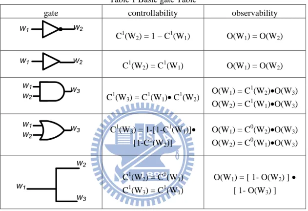
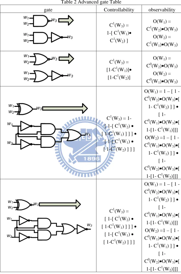
COP denotes “controllability and observability procedure,” one of the probabilistic testability analysis methods with the computing complexity of O(n). According to Table 1, Table 2 and Fig. 4.2(a), We first compute the controllability values and then use the controllability values to derive the observability values.]
Table 1 Basic gate Table
gate controllability observability
w1 w2 C1(W2) = 1 – C1(W1) O(W1) = O(W2) w1 w2 C1 (W2) = C1(W1) O(W1) = O(W2) C1(W3) = C1(W1)• C1(W2) O(W1) = C1(W2)•O(W3) O(W2) = C1(W1)•O(W3) C1(W3) = 1-[1-C1(W1)]• [1-C1(W2)] O(W1) = C0(W2)•O(W3) O(W2) = C0(W1)•O(W3) C1(W2) = C1(W1) C1(W3) = C1(W1) O(W1) = [ 1- O(W2) ] • [ 1- O(W3) ]
16
Table 2 Advanced gate Table
gate Controllability observability
C1(W3) = 1-[ C1(W1)• C1(W2) ] O(W1) = C1(W2)•O(W3) O(W2) = C1(W1)•O(W3) C1(W3) = [1-C1(W1)]• [1-C1(W2)] O(W1) = C0(W2)•O(W3) O(W2) = C0(W1)•O(W3) C1(W3) = 1- [ 1-[ C1(W2) • [ 1-C1(W1) ] ] ] • [ 1-[ C1(W1) • [ 1-C1(W2) ] ] ] O(W1) = 1 – [ 1 - C0(W2)•O(W3)•[ 1- C1(W2) ] ] • [ 1- C0(W1)•O(W3)•[ 1-[1- C1(W1)]]] O(W2) =1 – [ 1 - C0(W1)•O(W3)•[ 1- C1(W1) ] ] • [ 1- C0(W2)•O(W3)•[ 1-[1- C1(W2)]]] C1(W3) = [ 1-[ C1(W2) • [ 1-C1(W1) ] ] ] • [ 1-[ C1(W1) • [ 1-C1(W2) ] ] ] O(W1) = 1 – [ 1 - C0(W2)•O(W3)•[ 1- C1(W2) ] ] • [ 1- C0(W1)•O(W3)•[ 1-[1- C1(W1)]]] O(W2) =1 – [ 1 - C0(W1)•O(W3)•[ 1- C1(W1) ] ] • [ 1- C0(W2)•O(W3)•[ 1-[1- C1(W2)]]]
17
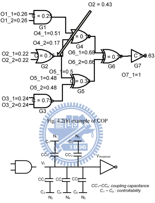
and observability values of the circuit are computed based on the former tables.
G1 G2 G4 G3 G5 G6 G7 C = 0.25 C = 0.75 C = 0.19 C = 0.75 C = 0.34 C = 0.37 C = 0.63 O1_1=0.26 O1_2=0.26 O2_1=0.22 O3_1=0.24 O4_1=0.51 O4_2=0.17 O5_1=0.5 O5_1=0.48 O5_2=0.48 O6_1=0.68 O6_2=0.66 O7_1=1 O2 = 0.43 O2_2=0.22 O3_2=0.24
Fig. 4.2(b) example of COP
threshold f
or
V
CC
CC
CC
CC
CC
CC
C
CC
C
CC
C
CC
C
CC
C
V
>
<
+
+
+
+
×
+
×
+
×
+
×
+
×
=
5 4 3 2 1 5 5 4 4 3 3 2 2 1 1Fig. 4.3 expected voltage value
The second step in our ATPG flow takes physical information including the circuit layout and extracted RC values into consideration. We reuse the controllability and observability values computed in the first step to estimate the expected voltage value for such floating net. First, every neighbor’s controllability multiplied by its coupling capacitance is summed up, then multiplied by such ratio with Vdd and the computed voltage is compared
18
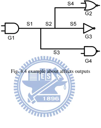
with the threshold of the driven gate to determine the logic value. If the computed voltage is bigger, logic-1 is justified on the driven gate. Otherwise, logic-0 is justified. Using the probability point of view to determine the logic value to be justified on the driven gate can speed up the ATPG process. Since the logic value of each neighboring net can be 0 or 1 with its individual probability, we incorporate the information to help determine the logic value of one driven gate. Fig. 4.4 shows an example. The target net can be coupled by five aggressors, N1 to N5, and their controllability values as well as the coupling capacitance values jointly determine the floating-net voltage, Vf.
19
The third step is to decide the target logic value to be justified. The step is different from previous open-segment ATPGs which target the segment as defect locations. We choose the branch segment connecting to a driven gate as one target to generate patterns. Fig. 4.4 shows an example. Gate G1 is connected with three fanout gates, G2, G3 and G4, and the net can be divided into five corresponding segments, S1, S2, S3, S4 and S5. Since previous open-segment ATPGs generate patterns for each segment defect, so in this example five patterns are generated. Instead, our flow generates only three patterns for G2, G3 and G4, respectively for diagnosis. The idea behind is not only to guarantee an faulty effects appearing at the input of the driven gate but also to enhance the diagnosis resolution.
20
Fig. 4.5(b) Example of a branch-and-bound tree
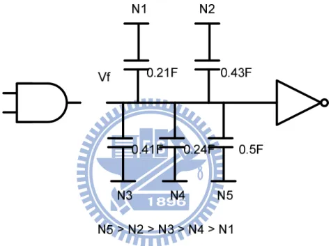
After choosing the target defect and evaluating the probabilities of logic values to be justified, a branch-and-bound algorithm is performed. The forth step of the flow is to construct and explore the coupling tree. It sorts the neighbors of the target defect by comparing their coupling-capacitance values first, and assigns the logic values in this order. The key idea is first to decide the logic value for the coupling net with a large capacitance which can save time on the exploration of the coupling tree and can derive the coupling net combination easier. Fig. 4.5(a) shows a example. If gate, G1 has five neighbors, N1 to N5 with the coupling-capacitance ranking as N5 > N2 > N3 > N4 > N1, Fig. 4.5(b) shows the assignments of logic values in the corresponding order.
N5 N2 1 1 N3 0.5 (N5) + 0.43 (N2) 0.21(N1) + 0.43(N2) + 0.41(N3) + 0.24(N4) + 0.5(N5) X1.8 = 0.935 > 0.85(threshold)
21
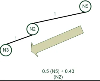
After having the order for the assignments, we start to give the logic value for the neighboring nets. The fifth step aims to find a feasible combination of all coupling nets which can induce a proper floating-net voltage bigger than the threshold voltage of the target driven gate. For example, if we choose logic-1 to be justified, a legal coupling-net combination has the sum of coupling capacitances from logic-1 neighbors divided by the sum of total coupling capacitances then multiplied by VDD bigger than the threshold voltage of the target driven gate. We show an example in Fig. 4.5(c). As both N5 and N2 are assigned logic-1, the corresponding floating-net voltage is larger than the threshold voltage of G2 and thus makes G2 receive logic-1. Then a feasible combination of coupling nets is found and shown as Fig. 4.5(d).
Fig. 4.5(d) change other nets combinations
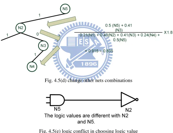
Fig. 4.5(e) logic conflict in choosing logic value
After the combination of coupling nets is decided by the previous step, then we can check whether such combination can satisfy the functionality from the circuit structure or not. The sixth step applies a SAT solver to mainly check the coupling-net combination again the functionality of the circuit. If the result return SAT, it means there is no conflict among the assignment of the coupling nets. If UNSAT is returned, the combination is infeasible. Fig. 4.5(e) indicates that N5 and N2 cannot have logic-1 at the same time. When we assign logic-1
22
to both of them, UNSAT is returned and make us check whether we explore 2N times for this type of justification or no. Note that N is the number of neighbors. If 2N is reached, we classified this defect as pseudo-untestable. If not, more combinations are explored. Fig. 4.5(b) shows the coupling tree. When assigning N5 and N2 to logic-1 is UNSAT, an alternative combination should be explored until 2N times are reached. The whole process is illustrated in Fig. 4.5(f).
Fig. 4.5(f) aborted fault
After ensuring the activation of an faulty effect induced by the combination of coupling nets, we then check if the faulty effect can propagate to any output. The seventh step is done by SAT solving of coupling-net combination over a miter circuit that combines the faulty and fault free circuits shown as Fig 4.5(g).
23
fault
Check the fault activation.
Fig. 4.5(g) check the fault activation
OX1
OX2
OXN
O = 1 Faulty circuit
Fault free circuit faults
24
Fig. 4.5(h) check the fault propagation
The miter circuit combines the faulty and fault-free circuits with proper XOR gates into a new circuit as shown as Fig. 4.5(h). A SAT engine is performed on the corresponding CNF form for such miter. If SAT is returned, the faulty effect can successfully propagate to at least one output and a legal pattern is found. If UNSAT is returned, the faulty effect is blocked during the propagation and cannot be observed at any output. When an UNSAT occurs, we repeat trying up to 2N times for this coupling-net combination.
S1 S2 S3 S4 S5 G1 G2 G3 G4
Focus on G1's output G2, generate pattern P1 and Xor results XO1 0 0 0 0 0 0 P1 golden 1 0 0 0 0 0 Sim result
25
Fig. 4.5(j) Example of check robustness
When a pattern is successfully generated, our last step will check its robustness. We use the pattern to run fault simulation with the injection of the target defect, and then check whether output responses match the expected values under this pattern or not. If yes, the pattern as well as its information is stored for diagnosis. If not, the pattern is removed. Fig. 4.5(i) and Fig. 4.5(j) illustrate the step.
26
Chapter 5
27
start
Construct open segment candidates
Error output responses
Diagnosistic pattern
Pick one net candidate defect
Simulate physical information
Match output?
Collect True candidate Until injecting last open
segment candidates True candidate open segment defects Yes No end
Fig. 5.1 Diagnosis flow
After the diagnostic ATPG, the information about patterns and its matching outputs is available. Under the single defect assumption, we can diagnose the faulty circuit by a diagnosis flow shown in Fig. 5.1 and the proposed diagnosis flow can achieve high resolution.
28
Fig. 5.2 Divide diagnosis flow into two stages
This flow mainly consists of two steps which are illustrated in Fig. 5.2: the first one is dictionary-based diagnosis and the second one is inject-and-evaluate diagnosis.
S1 S2 S3 S4 S5 G1 G2 G3 G4
Real defect occurs in S2
Fig. 5.3(a) defect occur in S2
29
Fig. 5.3(c) Pattern, P3 and its output result O3
The diagnosis flow starts after deriving the diagnostic patterns for the circuit under test. Correct logic values for all outputs can be obtained from the simulation. The first step is to construct open-segment candidates. We can get all faulty gate candidates by matching the real outputs and the patterns included in the diagnostic pattern information. Because the proposed ATPG targets the gate not the segment, we combine the faulty gate candidates to derive the corresponding faulty segments. This method can be viewed as one of the dictionary diagnosis approaches. Here shows an example. Fig. 5.3(a) shows a real defect that occurs on segment 2 (denoted as S2) driven by the gate G1. We apply all the patterns generated from our ATPG to testing and record the output responses. As S2 is open, two out of our diagnostic patterns will result in the error outputs and Fig. 5.3(b) and (c) show these two cases. Because the open S2 can affect gate G2 and gate G3 only, the pattern for G4 should not result in any error output shown as Fig. 5.3(d). With our diagnostic patterns and matching information, we can compose the defect location in Fig. 5.3(e).
30 S1 S2 S3 S4 S5 G1 G2 G3 G4 Using the faulty gates information to
backtrace the defect
X
O
X
Fig. 5.3(e) backtrace to the defect
Multiple open-segment candidates can be obtained from the first step. Next, we perform the silicon diagnosis in an inject-and-evaluate manner. During such second step, we choose one defect candidate at a time for injection and run simulation with the assistance of physical information. At the end, whether a candidate is a true or not depends on whether the simulation result matches the real silicon output result or not. If not, such defect candidate is eliminated. If yes, it remains in the defect pool as shown in Fig. 5.4 for silicon inspection in the future.
31
Real defect
Patterns Output results
Estimation defect
Patterns Output results
Estimation defect
Patterns Output results
Compare with output results
Match the estimate defect output and real defect output exactly
32
Chapter 6
33
Table 3 circuit information
circuit #net #m-f net #seg C432 203 89 443 C499 275 59 566 C880 468 125 979 C1355 619 259 1404 C1908 938 385 1893 C2670 1642 454 2821 C3540 1741 579 3781
The experiments are conducted on the ISCAS85 benchmark circuits. The ISCAS 85 benchmark circuits, layouts and coupling capacitance information are available from TAMU websites [34]. The ISCAS 85 benchmark circuits are synthesized with a 5-metal-layer TSMC 180 nm CMOS technology. The threshold voltage of each type of gate is determined through SPICE simulation. For ATPG, we use a SAT solver named MiniSat 2.0 which is one of the best SAT solvers in practice. MiniSAT 2.0 is a fast complete SAT solvers and the source code is open for public.
Table 3 shows the gate-level and physical information of the ISCAS 85 circuit: the second row denotes the total number of nets; the third row denotes the number of nets with multiple fanouts; the forth denotes the total number of segments according to the layout of the circuits.
During the ATPG step, the testability of the circuit is incorporated in the-branch and-bound method. The original version of the-branch-and-bound method is proposed by Spinner [26], and always chooses logic-1 then logic-0 to justify (1->0). If the ATPG for justifying logic-1 fails, the algorithm will change to justify logic-0. Obviously, it is not necessarily better to start with logic-1. Therefore, three other different strategies are also proposed to guide the ATPG process: (1) 0->1: logic-0 is first justified and then logic-1; (2) controllability: the controllability values of the coupling nets for the target segment can determines the expected logic value of the target segment to be justified; (3) observability: the observability value of the target segment determines the logic value to be justified.
Table 4 shows the runtime comparison of using the above 4 different strategies on some small ISCAS85 circuits. The first column shows the name of the circuits and column 2, 3, 4 and 5 shows the runtime in seconds for the 1->0, 0->1, observability and controllability strategies, respectively. As you can see, the 1->0 strategy is not necessarily superior. Especially when the circuit size goes larger, the observability and controllability strategies both have better efficiency over the 1->0 strategy. Therefore, the observability strategy is
34
chosen to be incoportated in our ATPG algorithm.
Table 4 compare with other ATPG
circuit 1->0 0->1 observation controllability
c432 46 137 75 97
c499 497 542 507 470 c880 299 330 267 312 c1355 1124 993 873 884
After the ATPG process completes successfully, defects can be further classified into different categories, and Table 5 shows the statistics. The first column shows the number of
ATPG-untestable defects which means that no pattern can be generated after trying the 2N or
all possible combinations of the coupling nets for the target segment defect. The second column shows the number of aborted defects, which are defined as after trying up to five times the generated pattern cannot result in matching output responses with those from the physical simulation. The third and forth columns show the numbers of no-coupling defects and no-segment defects, respectively. Both categories are also classified as the structurally
untestable. The last column shows the numbers for successful defects where a pattern can be
successfully generated by the ATPG process.
Table 5 fault classification
circuit ATPG-
untestable aborted no-coupling no-segment successful
c432 15 4 28 7 292 c499 79 19 36 32 303 c880 30 3 98 26 615 c1355 170 32 138 32 729 c1908 293 2 195 25 1000 c2670 243 31 198 140 1801 c3540 453 14 269 22 2170
After generating diagnostic patterns and collecting the pattern information, the diagnosis step proceeds and the experimental result is shown in Table 6. The first column represents the total runtime for diagnosis. Since the proposed diagnosis algorithm is dictionary-based, it runs efficiently. The second column represents the numbers of detected defects. In our experiments, 100 random defects are injected onto the circuit under test individually and 91 defects can be detected by our algorithm. The third column represents the number of candidate defects
35
reported by our diagnosis algorithm. For example, for c432, 91 defects are detected and only 91 candidate defects are reported, correspondingly. After checking the candidates against the injected defects, they are perfectly matched. The forth column represents the diagnosis resolution which is computed as the number of candidates divided by the number of injected defects. For example, the resolution is 1 for c432 and it means that our algorithm can find the exact defect on every defective circuit. The last column represents the total number of generated patterns. Note that we do not apply any compaction or compression technique on the pattern set and thus pattern reduction can be one of the future directions of this work.
Table 6: Diagnosis results
circuit Ddtime(s) detected candidate resolution # patterns c432 11.584 91 91 1 292 c499 16.013 73 74 1.01 303 c880 41.526 83 84 1.01 615 c1355 145.753 70 70 1 729 c1908 91.917 68 68 1 1000 c2670 259.844 70 73 1.04 1801 c3540 445.219 79 79 1 2170
To fairly compare our diagnostic patterns and the diagnosis flow with other conventional random and 5-detect stuck-at patterns, in Fig 6.1 we also develop a dictionary-based diagnosis flow which consists of two parts: (1) the generation of the defect dictionary and (2) dictionary comparison.
36
Fig. 6.1 diagnosis flow for random patterns and 5-detection patterns
The first part of such flow applies the patterns set for simulation with the assistance of physical information against all possible defects. All the falling patterns and the related information including faulty driven gates, faulty segments and output syndromes are recorded to build a dictionary for diagnosis.
The second part of the flow is dictionary diagnosis. We first sample 100 same circuits with random injection of defects. After defect injection, we run the simulation with physical information. The third step validate whether the defect dictionary matches the output responses from the physical simulation on each pattern. If yes, the counts of defects are checked. Otherwise, we skip to the next pattern. If the count for one defect is equal to the expected value from the dictionary, such defect is saved as a true defect. Otherwise, it is removed.
Table 7 shows the information about the pattern sizes and their dictionary sizes for random patterns and 5-detect patterns. The total numbers of random patterns used in our experiments are 1000 while the 5-detect patterns are generated by a commercial tools with proper modifications.
37
Table 7: random patterns and 5-detection pattern fault dictionary
circuit # random patterns random pattern dictionary # 5-detection patterns 5-detect pattern dictionary c432 1000 42688 617 29033 c499 1000 92501 794 105195 c880 1000 168376 476 92055 c1355 1000 197062 1272 432926 c1908 1000 290561 1725 643695 c2670 1000 500262 786 410883 c3540 1000 429523 1465 638965
After applying the diagnosis flow, we can obtain the following two tables. Table 8 shows the diagnosis results for 5-detect patterns whereas Table 9 shows the results for random patterns. Column 1 shows the circuit name and column 2 shows the runtime required by the diagnosis process. Column 3 and 4 reports the numbers of defected defects and reported candidates whereas resolution in column 5 is computed by column 4 divided / column 3. Column 5 shows the total number of patterns used for diagnosis.
38
Table 8: 5-detection patterns diagnosis result
circuit Ddtime(s) # detected #
candidates resolution #patterns c432 107.883 92 148 1.6 617 c499 613.446 77 262 3.4 794 c880 340.501 86 123 1.43 476 c1355 4093.384 80 232 2.9 1272 c1908 7565.367 75 240 3.2 1725 c2670 3126.143 75 182 2.43 786 c3540 6898.963 83 208 2.51 1465
Table 9: random pattern diagnosis results
circuit Ddtime(s) # detected #
candidates resolution #patterns c432 265.441 92 148 1.6 1000 c499 792.886 75 396 5.28 1000 c880 1260.463 85 125 1.47 1000 c1355 1480.233 80 291 5.74 1000 c1908 1942.933 70 419 5.99 1000 c2670 4624.633 64 267 4.17 1000 c3540 3070.196 70 392 5.6 1000
By comparing Table 8 and Table 9 with Table 6, we can observe that the proposed diagnosis with the diagnostic patterns run much faster than the dictionary-based diagnosis using random and/or 5-detect stuck-at patterns. Also, the result in Table 7 is worse than the other two on the numbers of detected defects. Besides the limitation due to the SAT solving in the ATPG process, there are two more limitations in the proposed flow: one is the success out of 2N trials in the-branch-and-bound search to derive a feasible coupling-net combination and the other is the success out of 5 trials in fault propagation of physical simulation to observe expected output responses. Both failures create extra un-diagnosable defects which are excluded from the defect dictionary. Comparing with the forth and the fifth columns in Table 7, apparently our diagnostic patterns with the proposed diagnostic flow can reach better resolutions for all benchmark circuits.
39
Chapter 7
Conclusion
40
When an open defect occurs on a segment of the circuit, physical characteristics of the circuit such as the layout and the cell library cause dynamic faulty behaviors under different input patterns. Such phenomenon is called Byzantine effect which makes open-segment defects not easy to be detected. Previous researches about open-segment defects mainly focus on ATPG and the diagnosis techniques and do not address the diagnosability of test patterns properly. The test set with high defect coverage does not necessarily accompany good diagnosability. Therefore, we are motivated to develop a two-stage algorithm including diagnostic ATPG and its diagnosis flow in the thesis.
The first stage for diagnostic ATPG aims to generate the patterns for all open-segment defects and consists of three steps: (1) finding a feasible coupling-net combination, (2) justifying a pattern conforming to the coupling-net combination, and (3) validating output responses through physical simulation. Branch-and-bound search, testability analysis and SAT solving techniques are integrated during this stage. Particularly, our indirect diagnostic ATPG targets each driven gate of the open segment instead of the segment itself, and greatly reduces the pattern size as well as the total runtime. In the second stage for diagnosis, defect candidates are composed according to information obtained during the previous stage in a dictionary fashion. As a result, only very few candidates are reported. Last, a inject-and-evaluate approach is applied to remove those candidates failing to match output responses against all patterns.
Experiments are conducted on ISCAS85 benchmark circuits and the result explains the effectiveness and efficiency of the proposed algorithm. For all ISCAS85 circuits, nearly 1 candidate that exactly matches the injected defect can be reported for each defective sample. Due to the indirect diagnostic ATPG, the pattern size as well as the total runtime (including ATPG and diagnosis) is greatly reduced. The overall performance in terms of time is about 10X better than that from previous researches. However, some aborted defects may escape from our diagnostic ATPG pattern set and thus become our future work.
Other future directions include: (1) extending our algorithm to handle multiple defects, (2) applying pattern compaction and compression to further reduce pattern size, and (3) improving the timing performance by the replace of a better SAT solving engine.
41
Bibliography
1. Jaume, S. and F.H. Charles, CMOS Electronics: How It Works, How It Fails. 2004: John Wiley \& Sons.
2. Huang, S.Y., Diagnosis of Byzantine Open-Segment Faults, in Test Symposium, 2002.
Proceedings. 11th Asian. 2002. p. 248-253.
3. Wei, Z., C. Wu-Tung, and S.M. Reddy. Interconnect Open Defect Diagnosis with
Physical Information. in Test Symposium, 2006. ATS '06. 15th Asian. 2006.
4. Laung-Terng, W., C.-W. WU, and X. WEN, eds. VLSI Test Principles and
Architectures: Design for Testability. 2006, Elsevier Morgan Kaufmann Publishers:
Boston.
5. Tafertshofer, P. and A. Ganz. SAT based ATPG using fast justification and
propagation in the implication graph. in Computer-Aided Design, 1999. Digest of Technical Papers. 1999 IEEE/ACM International Conference on. 1999.
6. Roth, J., Diagnosis of automata failures: A calculus and a methods. 1966, IBM. p. 278-291.
7. Goel, P., an implicit enumeration algorithm to generate tests for combinational logic
circuits. IEEE Trans. Comput, 1981: p. 215-222.
8. Larrabee, T., Test pattern generation using Boolean satisfiability. Computer-Aided Design of Integrated Circuits and Systems, IEEE Transactions on, 1992. 11(1): p. 4-15.
9. Chess, B. and T. Larrabee, Creating small fault dictionaries [logic circuit fault
diagnosis]. Computer-Aided Design of Integrated Circuits and Systems, IEEE
Transactions on, 1999. 18(3): p. 346-356.
10. Jue, W. and E.M. Rudnick, Bridge fault diagnosis using stuck-at fault simulation. Computer-Aided Design of Integrated Circuits and Systems, IEEE Transactions on, 2000. 19(4): p. 489-495.
11. Abramovici, M., P.R. Menon, and D.T. Miller, Critical Path Tracing: An Alternative
to Fault Simulation. Design & Test of Computers, IEEE, 1984. 1(1): p. 83-93.
12. Waicukauski, J.A. and E. Lindbloom, Failure diagnosis of structured VLSI. Design & Test of Computers, IEEE, 1989. 6(4): p. 49-60.
13. Kuehlmann, A., et al. Error Diagnosis for Transistor-Level Verification. in Design
Automation, 1994. 31st Conference on. 1994.
14. Shi-Yu, H., et al. ErrorTracer: a fault simulation-based approach to design error
diagnosis. in Test Conference, 1997. Proceedings., International. 1997.
15. Shi-Yu, H. On improving the accuracy of multiple defect diagnosis. in VLSI Test
Symposium, 19th IEEE Proceedings on. VTS 2001. 2001.
16. Fujiwara, H. and T. Shimono, On the Acceleration of Test Generation Algorithms. Computers, IEEE Transactions on, 1983. C-32(12): p. 1137-1144.
17. Pomeranz, I. and S.M. Reddy. On the generation of small dictionaries for fault
location. in Computer-Aided Design, 1992. ICCAD-92. Digest of Technical Papers., 1992 IEEE/ACM International Conference on. 1992.
18. Camurati, P., et al. A diagnostic test pattern generation algorithm. in Test Conference,
1990. Proceedings., International. 1990.
19. Hartanto, I., et al. Diagnostic test pattern generation for sequential circuits. in VLSI
42
20. Xue, H., C. Di, and J.A.G. Jess. Probability analysis for CMOS floating gate faults. in
European Design and Test Conference, 1994. EDAC, The European Conference on Design Automation. ETC European Test Conference. EUROASIC, The European Event in ASIC Design, Proceedings. 1994.
21. Rodriguez-Montanes, R., et al. Diagnosis of Full Open Defects in Interconnecting
Lines. in VLSI Test Symposium, 2007. 25th IEEE. 2007.
22. Needham, W., C. Prunty, and Y. Eng Hong. High volume microprocessor test escapes,
an analysis of defects our tests are missing. in Test Conference, 1998. Proceedings., International. 1998.
23. Henderson, C.L., J.M. Soden, and C.F. Hawkins. THE BEHAVIOR AND TESTING
IMPLICATIONS OF CMOS IC LOGIC GATE OPEN CIRCUITS. in Test Conference, 1991, Proceedings., International. 1991.
24. Makki, R.Z., S. Shyang-Tai, and T. Nagle. Transient power supply current testing of
digital CMOS circuits. in Test Conference, 1995. Proceedings., International. 1995.
25. Konuk, H., Voltage- and current-based fault simulation for interconnect open defects. Computer-Aided Design of Integrated Circuits and Systems, IEEE Transactions on, 1999. 18(12): p. 1768-1779.
26. Spinner, S., et al. Automatic Test Pattern Generation for Interconnect Open Defects. in VLSI Test Symposium, 2008. VTS 2008. 26th IEEE. 2008.
27. Xijiang, L. and J. Rajski. Test Generation for Interconnect Opens. in Test Conference,
2008. ITC 2008. IEEE International. 2008.
28. Hillebrecht, S., et al. Extraction, Simulation and Test Generation for Interconnect
Open Defects Based on Enhanced Aggressor-Victim Model. in Test Conference, 2008. ITC 2008. IEEE International. 2008.
29. Devtaprasanna, N., et al. Test Generation for Open Defects in CMOS Circuits. in
Defect and Fault Tolerance in VLSI Systems, 2006. DFT '06. 21st IEEE International Symposium on. 2006.
30. Gomez, R., A. Giron, and V.H. Champac, A Test Generation Methodology for
Interconnection Opens Considering Signals at the Coupled Lines. J Electron Test,
2008: p. 529-538.
31. Shi-Yu, H. Diagnosis of Byzantine open-segment faults [scan testing]. in Test
Symposium, 2002. (ATS '02). Proceedings of the 11th Asian. 2002.
32. Chen-Yuan, K., L. Chien-Hui, and C.H.P. Wen. An ILP-Based Diagnosis Framework
for Multiple Open-Segment Defects. in Microprocessor Test and Verification (MTV), 2009 10th International Workshop on. 2009.
33. Renovell, M. and G.N. Cambon, Electrical analysis and modeling of floating-gate
fault. Computer-Aided Design of Integrated Circuits and Systems, IEEE Transactions
on, 1992. 11(11): p. 1450-1458.
34. Lu, X. and W. Shi. Layout and Parasitic Information for ISCAS Circuits. 2004 [cited; Available from: http://dropzone.tamu.edu/~xiang/iscas.html.