行政院國家科學委員會補助專題研究計畫成果報告
※※※※※※※※※※※※※※※※※※※※※※※※※
※ ※
※
高均勻載子移動率之低溫複晶矽薄膜電晶體研製
※
※ ※
※
※
※※※※※※※※※※※※※※※※※※※※※※※※※
計畫類別:■個別型計畫
□整合型計畫
計畫編號:NSC 90-2215-E-009-068
執行期間: 90 年 8 月 1 日至 91 年 10 月 31 日
計畫主持人:鄭晃忠 國立交通大學電子工程學系
共同主持人:
計畫參與人員:林敬偉、張原熏、常鼎國
國立交通大學電子工程學系
本成果報告包括以下應繳交之附件:
□赴國外出差或研習心得報告一份
□赴大陸地區出差或研習心得報告一份
□出席國際學術會議心得報告及發表之論文各一份
□國際合作研究計畫國外研究報告書一份
執行單位:國立交通大學電子工程學系
中
華
民
國
91 年 10 月 31 日
高均勻載子移動率之低溫複晶矽薄膜電晶體研製
Fabrication of Uniform and High Mobility
Low Temperature Poly-Si TFTs
計畫編號:NSC
90-2215-E-009-068
執行期限:90 年 8 月 1 日至 91 年 10 月 31 日
主持人:鄭晃忠 國立交通大學電子工程學系
計畫參與人員:林敬偉、張原熏、常鼎國
國立交通大學電子工程學系
中文摘要 為了要進一步改善複晶矽薄膜的結晶 性、低溫複晶矽薄膜電晶體之電特性及避 免傳統準分子雷射結晶與鎳金屬催化結晶 法的缺點,我們提出一種新穎的結晶方 式。當適當的控制雷射能量,結合準分子 雷射與鎳金屬催化結晶法可製作出高品質 之複晶矽薄膜。經由鎳金屬催化結晶法製 備出之複晶矽薄膜具有較大的晶粒但其內 部所含缺陷較多,而利用準分子雷射後處 理可以減少這些缺陷同時維持原有晶粒的 大小。利用這種方式做出之低溫複晶矽薄 膜 電 晶 體 其 載 子 移 動 率 可 以 到 達 300 cm2/V*s 同時具有較佳的均勻性。 AbstractIn order to further improve the quality of crystallized poly-Si thin films and the performance of LTPS TFTs, and avoid the drawbacks of conventional ELC and Ni-MILC process, a novel crystallization method is subsequently proposed. A high-quality poly-Si thin film with large grains could be produced by a combination of Ni-MILC and ELA processes if the post ELA process is properly controlled. The Ni-MILC process is initially used to produce a poly-Si thin film with very large but defect-rich grains and the post ELA process subsequently reduces the intra-grain defects while keeping the grain size large. LTPS TFTs with field-effect mobility exceeding 300 cm2/V*s have been fabricated by using this method, while exhibit good uniformity.
Reasons and Purposes
Nickel metal-induced lateral crystallization (Ni-MILC) of amorphous silicon (a-Si) thin film has been utilized to fabricate good-performance low-temperature polycrystalline silicon (LTPS) thin film transistors (TFTs). By means of proper selection of device layout and process parameters, such as film thickness, shape and length of Ni seeding window, and distance between Ni seeding window and TFT channel, LTPS TFTs with improved performance and good uniformity have been fabricated. However, in spite of the above, the electrical characteristics of LTPS TFTs fabricated by Ni-MILC process are still inferior to those fabricated by excimer laser annealing (ELA) process. Besides the metal contamination in poly-Si, the possible reason should be attributed to the high defect density still existing in Ni-MILC poly-Si.
A post high-temperature annealing has been adopted to reduce the defect density in Ni-MILC poly-Si and enhance grain growth, and poly-Si TFTs fabricated using this method exhibited excellent performance [1][2]. However, such a high temperature annealing process (generally > 900°C) is not compatible with glass substrates, which is against the essential requirement for LTPS TFT technology.
In this report, a conceptual basis for the two-step annealing is first introduced, along with the experiments for the fabrication of LTPS TFTs by applying post laser annealing on Ni-MILC poly-Si thin film. Electrical
performance of the resulting devices is then reviewed, placing emphasis on the improvement in performance accompanying with good uniformity.
Experiments
The procedure of fabricating LTPS TFTs is illustrated in Fig. 1. A 450Å amorphous silicon layer was first deposited on an oxidized silicon substrate by LPCVD at 450°C. Ni-MILC was carried out subsequently at 550°C for several hours. The remaining Ni and capping oxide were removed completely after crystallization. After clean process, the wafer was then subjected to KrF excimer laser annealing at room temperature. Several laser energy densities and shot densities per area were adopted to investigate their effects on the TFT performance. After defining the device active layer, a 1000Å TEOS gate oxide was deposited by PECVD. A 3000-Å TaN film was then deposited by sputtering for gate electrode. The TaN and gate oxide were etched by reactive ion etching (RIE) to form gate electrodes. A self-aligned phosphorous implantation with dose of 5×1015 cm-2 was carried out to form source and drain regions. A passivation oxide layer was then deposited and the implanted dopants were activated by thermal annealing at 550°C for 12 h. Contact holes formation and metallization were carried out after dopants activation.
Results and Discussion
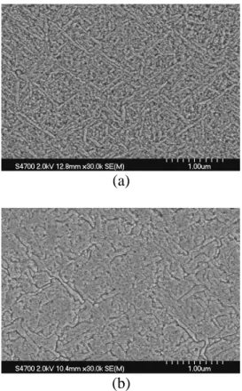
Figure 2 shows the SEM image of Secco-etched poly-Si thin film produced by Ni-MILC followed by post laser annealing. Only one distinct grain boundary is observed in the graph, and the actual grain size observed by SEM is tens of micrometers long. For comparison of the intra-grain microstructure, Fig. 3(a) and 3(b) show the magnified SEM images of Secco-etched poly-Si thin films produced by Ni-MILC and Ni-MILC followed by post laser annealing, respectively. It is observed that the Ni-MILC poly-Si thin film was full of defects and
low-angle grain boundaries. However, after laser annealing, most of the defects and low-angle grain boundaries between needlelike crystallites disappeared. Laser irradiation made the Ni-MILC poly-Si melting and subsequently re-solidify from the un-melted poly-Si, which provided the energy to repair the defects generating in Ni-MILC process and to merge the small grains separated by low-angle grain boundaries. Besides, as the applied laser energy density did not completely melt the crystallized poly-Si thin film, poly-Si would re-grow from the un-melted poly-Si seeds, and as a result, the microstructure of the laser-annealed poly-Si resembles that of un-annealed one.
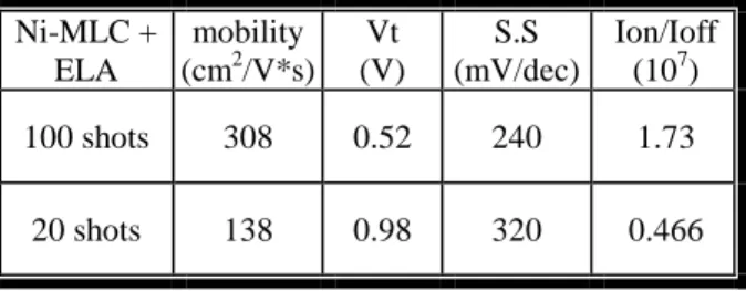
Figure 4 shows typical transfer characteristics of LTPS TFTs fabricated by applying laser annealing on Ni-MILC poly-Si thin films, in which the number of applied laser-shot per area was 20 and 100, and the laser energy density was optimized to obtain the best TFT performance. Table 1 also lists some importance electrical characteristics of the two devices. Increasing the number of applied laser-shot per area from 20 to 100 promoted the field effect mobility of LTPS TFTs from 138 to 308. Low threshold voltage and subthreshold swing were also obtained in both.
Figure 5(a)~5(b) display the dependence of electrical characteristics of LTPS TFTs on the applied laser energy density, in which the field effect mobility, threshold voltage, and subthreshold swing are included, respectively. In this case, the applied laser shot density per area was 100 and TFT dimension of W/L = 20 µm / 20 µm was measured. There is an optimal range of laser energy density for obtaining the best TFT performance, which is similar to the results reported by Murley et al. [4]. Field effect mobility of exceeding 200 cm2/V*s can be achieved when the applied laser energy density was controlled at 270 ~ 280 mJ/cm2. They imply that the performance of TFTs is related to the melting depth of poly-Si thin films. In order to obtain the best quality of poly-Si thin films, defects in poly-Si must be
removed entirely by melting most of the poly-Si thin film. As a result, precise control of applied laser energy density is also indispensable for this new process
Fig. 6(a) and 6(b) show the statistical distribution of the threshold voltage (VT) and
field effect mobility (µFE) of LTPS TFTs
fabricated by different crystallization manners, respectively. Twenty TFTs were measured in each case, and the laser energy density was controlled at nearly optimal value for those requiring laser annealing. Among the five crystallization manners used, the LTPS TFTs fabricated by a combination of Ni-MILC and ELA show much better performance and uniformity than those fabricated merely by either Ni-MILC or ELA of a-Si.
Conclusions
High-performance LTPS TFTs with good uniformity have been fabricated by combining the Ni-MILC and ELA process. The SEM image has shown that the grain size of the poly-Si thin film produced by the proposed method was tens of micrometers long, and the microstructure resembled the Ni-MILC one excluding the reduction of defect density. Laser energy density and number of laser shot have been shown to have a profound influence on the performance of resulting LTPS TFTs. By optimizing the laser process conditions, LTPS TFTs with field-effect mobility exceeding 300 cm2/V*s were fabricated. The performance and uniformity of LTPS TFTs fabricated by combining the Ni-MILC and ELA process were shown to be much superior to those of LTPS TFTs fabricated by merely either ELA or Ni-MILC process.
Reference
1.Hongmei Wang, Mansun Chan, SinghJagar, Vincent M. C. Poon, Ming Qin, Yangyuan Wang, and Ping K. Ko,IEEE Trans. Electron Devices, vol. 47, pp. 1580-1586, 2000.
2. Victor W. C. Chan, Philip C. H. Chan, and Mansun Chan, IEEE Trans. Electron Devices, vol. 48, pp. 1394-1399, 2001.
3. Victor W. C. Chan, Philip C. H. Chan, and Mansun
Chan, IEEE Trans. Electron Devices, vol. 48, pp. 1394-1399, 2001.
4. Darren Murley, Nigel Young, Michael Trainor, and David McCulloch, IEEE Trans. Electron Devices, vol. 48, pp. 1145-1151, 2001.
Table 1 Measured electrical characteristics of LTPS TFTs fabricated by applying laser annealing on Ni-MILC poly-Si thin films.
Ni-MLC + ELA mobility (cm2/V*s) Vt (V) S.S (mV/dec) Ion/Ioff (107) 100 shots 308 0.52 240 1.73 20 shots 138 0.98 320 0.466 a-Si oxide oxide Ni silicon wafer poly-Si oxide silicon wafer
excimer laser irradiation
poly-Si oxide silicon wafer oxide TaN N+ N+
Fig. 1 The process procedure of fabricating LTPS TFTs by applying post laser annealing on Ni-MILC poly-Si thin films.
Fig. 2 SEM image of Secco-etched poly-Si thin film produced by Ni-MILC followed by ELA.
(a)
(b)
Fig.3 Magnified SEM images of Secco-etched poly-Si thin films produced by (a) Ni-MILC and (b) Ni-MILC followed by post laser annealing.
-10 -5 0 5 10 15 20 10 -12 10 -11 10 -10 10 -9 10 -8 10 -7 10 -6 10 -5 10 -4 10 -3 Vds = 5.1V Vds = 0.1V W/L = 20µm/20µm Laser shots = 100 Laser shots = 20 Fi el d Ef fect M obi lit y (cm 2 /V*s ) D rai n C ur rent I d s ( A) Gate Voltage Vgs (V) 0 100 200 300 400 500
Fig. 4 Transfer characteristics of Ni-MILC + ELA LTPS TFTs
Fig. 5(a) The dependence of field effect mobility on the applied laser energy density
Fig. 5(b) The dependence of threshold voltage on the applied laser energy density.
Fig. 6(a) Statistical distribution of the threshold voltage of LTPS TFTs fabricated by different crystallization manners.
Fig. 6(b) Statistical distribution of the carrier mobility of LTPS TFTs fabricated by different crystallization manners.