566 IEEE ELECTRON DEVICE LETTERS, VOL. 16, NO. 12, DECEMBER 1995
the overlap between the gate and the n- region are about
0.08 pm and 0.03 pm, respectively. Both of the conventional S/D and the DDD MOSFET's have a n+ arsenic implant dose of 2.5 x cm-2. The n- phosphorus implant is
ffect
on
Band-Trap-Band Tunneling
A maximum substrate current stress method was adopted to obtain maximum interface trap generation and to minimize the oxide charge effects [SI. The stress conditions in the LDD,
conventional SD, and DDD MOSFET's were 1)
V,,
= 2.5 V, V& = 6.5 V, respectively. It should be mentioned that both of the S/D and DDD devices were stressed under approximately the same substrate current.Vd,
= 6v,
2)v,,
= 2.5v,
vds = 5.5v,
and 3)v,,
= 2.5v,
111. RESULTS AND DISCUSSIONS
Under a trap-assisted tunneling dominant condition, the increased drain leakage current can be derived as follows [ 6 ] : '
C e
rain Leakage in n-MOSFET's
Tahui Wang, Senior Member, IEEE,
T. E.
Chang,C.
Ne
Abstract-The structural dependence of the hot carrier stress
incurred drain leakage current via band-trap-band tunnelting
in off-state has been modeled and characterized in conven- tional S/D, DDD, and LDD n-MOSFET structures. The results
shows that lateral field enhanced band-trap-band tunneling b primarily responsible for an increased drain leakage current after hot carrier stress in LDD structures while vertical field induced tunneling is dominant in conventional S/D and DDD structures.
I. INTRODUCTION
ATE induced drain leakage (GIDL) current attributed to band-to-band tunneling has been found to be a major reliability issue in off-state MOSFET's [l], 121. Recently, much research interest has been attracted to the study of hot carrier stress effects
on
the GIDL [3]-[5]. In our earlier work, an interface trap-assisted tunneling and thermionic emis-sion model [6] has been developed to evaluate an increased drain leakage current after hot carrier stress. In the model, a complete band-trap-band leakage path is formed at the Si/SiOz interface by hole emission from interface traps to a valance band and electron emission from interface traps to a conduction band. It has been shown that, at a sufficiently large vdg, both electron and hole transitions are made through quantum tunneling. The two-step band-trap-band tunneling becomes increasingly important as the device dimension is further reduced since the vertical and the lateral electrical fields are continually increased in each generation of device scaling according to the generalized MOSFET scaling theory [7]. The trap-assisted leakage mechanism can be further divided into vertical field dominant tunneling and lateral field dominant tunneling. The features of these two tunneling processes are quite different. In this letter, the drain leakage currents via these two processes are characterized and modeled in a variety of MOSFET structures.
11. EXPERIMENT
To investigate the structural dependence of the band-trap- band tunneling process, three types of MOSFET structures, a Manuscript received February 27, 1995; revised August 29, 1995. This work was supported by the National Science Council, R.O.C., under Contract NSC84-2215-E009-006.
T. Wang, T. E. Chang, J. Y. Yang, K. M. Chang, and L. P. Chiang are with the Department of Electronics Engineering, Institute of Electronics, National Chiao-Tung University, Hsinchu 300, Taiwan, R.O.C.
C. M. Huang is with Macronix International Company, Technology Devel- opment Department, Hsinchu 300, Taiwan, R.O.C.
IEEE Log Number 9415618.
U
€hang,
J.
Y.
Yang,
K. M.
Chang,and L. P. Chiang
-5 -4 -3 -2 -5 -4 -3 -2 -5 -4 -3 -2 . Gate-to-Source Bins, Vgs (V)
Fig. 1.
leakage CurrentS due to interface traps in LDD, S D , and DDD MOSFET's. Measured (solid lines) and calculated (dashed lines) additional drain
0741-3106/95$04 00 0 1995 IEEE I
WANG et a1 STRUCTURAL EFFECT ON DRAIN LEAKAGE IN n-MOSFET’s 561 3 1 h
E
5
E
z
E
U W Q, 0 L# U Q, .I .y2
L:
LDDn-MOSFETv
= - 4 v :
25 2015
10
50
0.45
0.41
0.49 0.51
0.53 0.55
Position
(pm)
(a) h Y .r(I
e
2
A
E
8
Q h W Y .r(a
b
Q cr Ll Q) c) Uc
n 5100
2
S/D n-MOSFETv
=-4v
1 8060
40
20 01.8
1.84 1.88
1.92
1.96
2
Position
(pm)
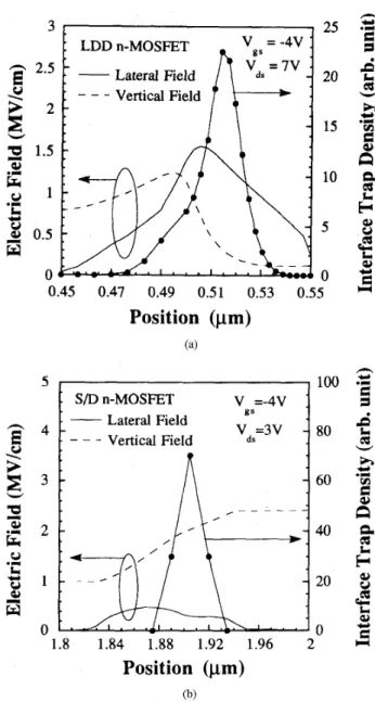
(b)Fig. 2. Vertical and lateral field distributions in (a) LDD and (b) S/D MOSFET’s. The gate edge is at 0.5 p m in the LDD device and at 2.0 pm in the S/D device.
(3)
where A is proportional to the interface trap density, F; is a
lateral field, F is a total field, and Et is the energy level of interface traps which are most effective in the band-trap-band tunneling process. Other variables have their usual definitions. It should be pointed out that if the lateral field is much greater than the vertical field, a theoretically lower limit of Btt about 13 MVkm is obtained and the corresponding Et is 0.5 ( E ,
+
Ew).
In the other extreme, if the vertical field is much larger than the lateral field,BZt
has a maximum value of 36 MVkm which is the same as the GIDL [9]. Thus, the valueDevice Structures B (MV/cm)
c
( X : interface traps) 31 - I G mI
35 DDD Post-stress--
Bit (MV/c:m) 1 3 - 15 23-
25 21 - 2 5 Dominant Reid in tunneling lateral field vertical field vertical field Fig. 3. MOSFET structures.Comparison of the band-trap-band tunneling characteristics in various
of B,t may vary significantly in different MOSFET structures depending on the relative strength of the vertical and lateral fields.
Fig. 1 shows the hot carrier stress induced drain leakage currents in the three structures. The soLid lines are from measurement and the dashed lines are from calculation (1). In the calculation, the field distributions are obtained from
a two-dimensional device simulation. The vertical and the lateral field distributions in the LDD and the S/D devices are plotted in Fig. 2. The gate edge is at 0.5 pm in Fig. 2(a) and at 2.0 pm in Fig. 2(b). The spatial ilistributions of the interface traps in the figure are evaluated from a numerical simulation [lo]. The schematic cross-sections of the structures, together with some important results, are compared in Fig. 3. In the LDD MOSFET, the interface traps are generated in the spacer region (i.e., outside the gate), where the lateral field is much larger than the vertical field. Thus, the lateral field induced tunneling is dominant and the obtained Btt is close to its theoretically lower limit 13 MV/cm. This value is
much lower than the pre-stress result. In the S/D MOSFET, however, the generated traps are located under the gate where the vertical field is stronger. As a result, the vertical field induced tunneling plays a more important role. The B,t reaches
a higher value about 23-25 MV/cm. In the DDD MOSFET, the interface traps are also generated under the gate during stress. The vertical field enhanced tunneling is dominant and the Btt value is again about 21
-
25 MV/cm. Furthermore, our study reveals that the interface traps in the DDD structure are located farther away from the maximum electric field than in the S / D structure in a measurement bias condition. This fact explains why the increased drain leakage current in the DDD MOSFET is much lower than that of the S/D MOSFET in Fig. 1 even though both devices were stressed under the same substrate current.In addition, the oxide charge effect on the drain leakage is evaluated through a device simulation. In the simulation, a certain amount of negative oxide charge (2 x 10” cm-’) is placed in the LDD spacer region. The simulation shows that the enhancement of the drain leakage current due to the oxide charge only is no more than 15% in the current structure. This
568
quantity is much smaller than the band-trap-band tunneling induced drain leakage current.
ACKNOWLEDGMENT
The authors would like to thank MXIC, UMC, and NDL for technical support.
REFERENCES
[ l ] J. Chen, T. Y. Chan, P. K. KO, and C. Hu, “Subbreakdown drain leakage current in MOSFET,” IEEE Electron Device Lett., vol. EDL-8,
pp. 515-517, 1987.
[2] T. Y. Chan, J. Chen, P. K. KO, and C. Hu, “The impact of gate-induced drain leakage current on MOSFET scaling,” IEDM Tech. Dig., pp. 721-124, 1981.
[3] H. Sasaki, M. Saitoh, and K. Hashimoto, “Hot-carrier induced drain leakage current in n-channel MOSFET,” IEDM Tech. Dig., pp. 726729,
1987.
[4] C. Duvvury, D. J. Redwine, and H. J. Stiegler, “Leakage current degradation in N-MOSFET’s due to hot-electron stress,” IEEE Electron Device Lett., vol. 9, pp. 579-581, 1988.
IEEE ELECTRON DEVICE LETTERS, VOL 16, NO 12, DECEMBER 1995
[5] G . Q. Lo, A. B. Joshi, and D.-L. Kwong, “Hot-carrier-stress effects on gate-induced drain leakage current in n-channel MOSFET’s,” IEEE Electron Device Lett., vol. 12, pp. 5-7, 1991.
[6] T. Wang, T. E. Chang, and C. Huang, “Interface trap induced thermionic and field emission current in off-state MOSFET’s,” IEDM Tech. Dig.,
pp. 161-164, 1994.
[7] G. Baccarani, R. H. Dennard and M. R. Wordeman, “Generalized scaling theory and its application to a 114 micrometer MOSFET design,” IEEE Trans. Electron Devices, vol. ED-31, pp. 452-462, 1984.
[SI B. Doyle, M. Bourcerie, J. C. Marchetaux and A. Boudou, “Interface state creation and charge trapping in the medium-to-high gate voltage range during hot-camer stressing of n-MOS transistors,” IEEE Trans. Electron Devices, vol. 37, pp. 744-154, 1990.
[9] S. A. Parke, J. E. Moon, H. C. Wann, P. K. KO, and C. Hu, “Design for suppression of gate-induced drain leakage in LDD MOSFET’s using a quasi-two-dimensional analytical model,” IEEE Trans. Electron Devices,
vol. 39, pp. 1694-1703, 1992.
[lo] T. Wang, C. Huang, P. Chou, S . Chung and T. E. Chang, “Effects of hot carrier induced interface state generation in submicron LDD MOSFET’s,” IEEE Trans. Electron Devices, vol. 41, pp, 1618-1622,