國立交通大學
材料科學與工程學研究所
博士論文
一維氧化鋅奈米結構之製備及其應用
Synthesis of One Dimensional Zinc Oxide
Nanostructure and their Applications
研 究 生:姚奕全
指導教授:曾俊元 博士
指導教授:林 鵬 博士
一維氧化鋅奈米結構之製備及其應用
Synthesis of One Dimensional Zinc Oxide Nanostructure and their
Applications
研 究 生:姚奕全 Student:I-Chuan Yao
指導教授:曾俊元 博士 Advisor:Dr. Tseung-Yuen Tseng
指導教授
林 鵬 博士 Advisor:Dr. Pang Lin
國立交通大學
材料科學與工程學系
博士論文
A Thesis
Submitted to Department of Materials Science and Engineering
College of Engineering
National Chiao Tung University
in Partial Fulfillment of the Requirements
for the Degree of
Doctor of Philosophy
in
Materials Science and Engineering
April 2012
Hsinchu, Taiwan, Republic of China
一維氧化鋅奈米結構之製備及其應用
研究生:姚奕全 指導教授:曾俊元 博士
研究生:姚奕全
指導教授:林 鵬 博士
國立交通大學
材料科學與工程學系博士班
摘 要
一維奈米材料由於其卓越的物理與化學特性使其成為近幾年重要之研究領 域,在許多一維材料中,氧化鋅由於獨特的光、電及壓電特性而具有廣泛的應用 性,成為近年來受矚目的研究方向,於本論文中,我們加入新的製程方法或技術 改善一維氧化鋅奈米結構之應用。實驗中,利用掃描式電子顯微鏡(SEM)和穿透 式電子顯微鏡(TEM)研究材料之微結構,並使用發光光譜儀(PL)與電流-電壓量測 系統分析其光性與電性。本論文依氧化鋅奈米結構之應用與實驗設計分成四部份。 第一部分,我們所提出的一個簡單的方法製備氧化鋅奈米尖錐陣列,使奈米尖錐 於 25-100 ℃的環境中具備有低的啟動電場、高的場效增益因子與穩定的場發射 特性。而優異的場發射特性主要來自於降低氧化鋅發射子本身的氧空缺濃度與小 角度的尖錐角度,此簡單的製程方法展現了極大的潛力應用於場發射元件與發光 元件上。第二部份,我們所提出的一個有趣的方法來製作氧化鋅-氧化錫核-殼奈 米線結構應用於氣體感測器上,此氧化鋅-氧化錫核-殼奈米線具備高的氫氣感測 特性,如在溫度 250 ℃時通入 200 ppm 的氫氣其敏感度高達 89%,而高敏感性主 要來自於氧化錫膜對於氫氣的完全反應所造成,我們認為利用兩階段成長的方式所製備的氧化鋅-氧化錫核-殼奈米線具備在氣體感測使用的潛力。第三部份,成 功的製備垂直佳且分布均勻的氧化鋅奈米柱於低成本、可撓的聚對苯二甲酸乙二 酯(PET)基板上,該元件能夠重複且穩定操作於強度 25-70 μW/cm2的紫外光的照 射且具備有快的反應時間與回覆時間。此外,元件具備機械可撓性、高可靠度與 不同層級的光反應,因而具備有極大的潛力應用於紫外光感測器上。第四部份, 成功的製備緻密且均勻的的鎵摻雜氧化鋅奈米柱薄膜/金/鈦/二氧化矽/p-型矽基 板的電阻式記憶體元件,此種記憶體元件具備可逆與穩定的操作於開/關狀態間 且具備有超過一百次的穩定度特性,而元件的轉態機制主要跟鎵摻雜氧化鋅奈米 柱與柱之間的氧空位細絲形成與斷裂有關。結果顯示,此一緻密的鎵摻雜氧化鋅 奈米柱薄膜在電阻式記憶體的研究中具備有極高的應用價值。
Synthesis of One Dimensional Zinc Oxide Nanostructure and their
Applications
Student: I-Chuan Yao Advisor: Dr. Tseung-Yuen Tseng
Student: I-Chuan Yao
Advisor: Dr. Pang Lin
Department of Materials Science and Engineering
National Chiao Tung University
ABSTRACT
One-dimensional nanostructers are a new class of advanced materials that have been receiving a lot of research interest in the last decade due to their superior physical and chemical properties. Among one-dimensional materials, zinc oxide (ZnO) is one of the most important materials and has attracted much interest in recent years, due to its unique optical, electrical, and piezoelectric properties and versatile applications. In this dissertation, we propose new methods or technologies to improve the applications of 1D ZnO nanostructure. Macrostructure of the samples was characterized by scanning electron microscopy (SEM) and high resolution transmission electron microscopy (HRTEM). The optical and electrical properties were investigated by photoluminescence (PL) and current–voltage (I–V) characterization. The main focus of this dissertation can be divided into four parts. In first part, we demonstrate a simple method to fabricate ZnO nanotip array, which exhibit low turn-on field, high field enhancement factor and stable field emission properties at 25-100 ℃. The good field emission properties are attributed to reduced oxygen vacancy concentration and small tip angle of ZnO emitters, which shows good
potential for developing field emission and light emiting devices. In the second part, we provide another interesting route of fabricating ZnO-SnO2 core-shell nanowires
for gas sensor applications. The ZnO-SnO2 core-shell nanowires exhibited good
hydrogen sensor performance, such as the sensitivity is up to 89% against 200 ppm hydrogen at 250℃. Such high sensitivity was believed to be controlled by the nanoscale SnO2 layer, which was determined from pinch-off and fully conductive
state. The ZnO-SnO2 core-shell nanostructures made by two-step chemical growth
have high potential for gas sensor application. In the third part, vertical well-aligned and uniform ZnO nanorods were successfully prepared on low cost and flexible PET polymer substrate by aqueous solution method under various growth conditions. The photocurrents can be repeatly and reproducibly switched by modulating UV exposure with power densities of 25-70 μW/cm2. The fast response time (100 sec) and rapid recovery time (120 sec) are achieved in UV turn-on/off switching measurements. Owing to the mechanical flexibility, nondestructive properties, high reliability and multilevel photoresponse, the well-aligned ZnO nanorods grown on transparent and flexible PET polymer substrates have high potential for UV photodetector applications. In the fourth part, vertically well-aligned and uniform Ga-doped ZnO (GZO) nanorod thin films were successfully grown on Au/Ti/SiO2/p-Si substrates,
which used to make resistive switching memory devices. Such memory devices can be reversibly switched between ON and OFF states, with a stable resistance ratio of 10 times, narrow dispersion of ON and OFF voltages, and good endurance performance of over 100 cycles. The resistive switching mechanism in this design is related to the formation and rupture of conducting filaments consisting of oxygen vacancies, occurred at interfaces between GZO nanorods (grain boundaries). Results show that the resulting compact GZO nanorod thin films have a high potential for
Acknowledgements
時光飛逝,求學的生涯轉眼間就告一段落,回首求學之路,心中沒有不捨, 有的只是說不盡的感激與祝福。因人生道路上所經歷的人、事、物的影響與引領, 逐步建構出現在與未來的我。 首先衷心地感謝指導教授曾俊元博士,在我求學的過程中所給予的教導和鼓 勵,並提供良好的學習環境與自由的空間,使我得以開拓視野學習新知,除了在 學識上有所增長之外,對於人生的規劃及待人處事的態度方面,亦受益良多,僅 此表達最誠摯的感謝與敬意。另外,也特別感謝另一位指導教授林鵬博士在不同 思考邏輯方面的啟發指導,增加我個人的思考層面與研究邏輯,使我能順利完成 學業。也感謝百忙之中抽空參加我論文口試的委員們,有了委員們專業的建議與 熱心的指導,才能使我的論文更佳的完備。 本篇論文之所以能順利完成,心中最想感謝的人是交大奈米中心的鍾怡娟小 姐除了在 TEM 上的教導之外,對於我遭遇困難與煩惱時給予我最大的幫助與建議, 著實讓我博士班的生涯中充滿許多能量與衝勁,對於妳的幫助心中充滿無限的感 謝之意;另外也要感謝交大奈米科技中心提供了一流的分析儀器與充滿歡笑的研 究團隊:劉翊筑小姐、李良箴小姐、賴良一先生與徐武達先生,有你們的陪伴真 的讓我的求學生涯中充滿了許多的歡笑與回憶。 此外,感謝 TTY LAB 與材料所的學長、同學與學弟妹在生活上與研究上的協 助,令我在交通大學的學生生活更加地豐富。群傑、志洋、孟漢學長與岱螢同學 在研究上的經驗與日常生活中的相處使我受惠良多;材料所的國璋、峻彥、雲閔 學長與伊茹學姐在實驗的討論與教導令我能更順利進行相關研究;博班的崇榮、 文碩與駿揚學弟希望你們多加把勁,早日聽到你們的好消息; TTY LAB 的宏全、 啟翔、志文、昱廷、盈賢、政漢、聖和與佑書等碩士班學弟妹們,求學生涯中你 們的陪伴都是我最珍貴的回憶;材料所的車牧龍、諶昱涵、徐明義、王智、涂弘 恩、李孝謙、許書豪、蔡沁穎、陳奎岳、胡勝翔及邱維剛等球友們,在生活中所帶給我的歡笑與陪伴,我都銘記在心,也衷心的祝福你們凡事順利、心想事成, 並願我們的友誼長存。同時也要感謝所有曾經幫助及關心我的朋友們,謝謝你們 的幫忙。 再者感謝交大奈米中心所提供設備與服務。其中特別感謝陳聯珠、鄭淑娟與 劉悅恩小姐在量測與材料分析技術上所提供的服務與討論,以及行政人員何惟梅 小姐在行政事務上的協助。另外也要感謝國科會在研究計畫經費上的補助。 最後我要感謝我父母-姚錫勳先生與姚黃麗卿女士,因為你們多年來的辛苦 教導與栽培才能有今天的我,讓我無生活上的負擔與壓力,能專心地完成學業。 也感謝哥哥-姚鈞譯,無時無刻地給予我溫暖的關懷,讓我在灰心與氣餒的時候 不被眼前的困難所打倒。 相信我對於自己的未來,會繼續保持的好奇心與努力, 創造出屬於自己的一片天空。 謹以此論文獻給所有在人生道路上幫助過我的人 姚奕全 壬辰 春 於 風城 交通大學
Chapter 1 Introduction
1-1.
Nanosturcture and nanotechnology………..
11-2.
ZnO material characteristics………
21-3.
Synthesis of zinc oxide nanostructures………
41-3-1
Vapor-liquid-solid method………...
41-3-2
Aqueous solution (Hydrothermal) growth method
61-3-3
Electrodeposition growth method……….
71-4.
Properties, potential applications of ZnO nanorod arrays
81-4-1
Field emission properties………...
91-4-2
Gas sensor and ultraviolet photodetectors…………
121-4-3
Resistive random access memory (RRAM)……….
141-5.
Optical properties of zinc oxide………...
171-6.
Outline of dissertation
17Chapter 2 Nano Tip Fabrication of Zinc Oxide Nanorods and
their Enhanced Field Emission Properties
Contents
Abstract (in Chinese)……….
iAbstract (in English)……….
iiiAcknowledgments……….
viContents……….
viiiTable Lists……….
xii2-1.
Introduction...
292-2.
Experimental method………...
302-3.
Results and discussion………...
312-3-1
Morphology and crystalline of ZnO seed layer……
312-3-2
Morphology and crystalline of ZnO nanorod
structure………
312-3-3
Field emission properties………...
332-4.
Conclusions...
35Chapter 3 Electrical Properties and Reliability of ZnO-based
Nanorod Current Emitters
3-1.
Introduction...
433-2.
Experimental method...
443-3.
Results and discussion………
453-3-1
Morphology, crystal structure, composition and
optical properties of ZnO nanorod array…………..
453-3-2
Field emission properties……….
483-4.
Conclusions...
50Chapter 4 Field Emission Properties and Reliability of ZnO
Nanorod, Nanopagoda, and Nanotip Current Emitters
4-1.
Introduction...
574-2.
Experimental method………...
584-3.
Results and discussion………...
594-3-1
Morphology, crystal structure, composition and
optical properties of ZnO nanorod, nanopagoda
4-3-2
Field emission properties……….
614-4.
Conclusions……….
64Chapter 5 Hydrogen Gas Sensors using ZnO-SnO
2Core-Shell
Nanostructure
5-1.
Introduction...
715-2.
Experimental method………...
725-3.
Results and discussion……….
735-3-1
Crystal structure, morphology and chemical
composition of as-grown ZnO and ZnO-SnO
2core-shell nanowires……….
735-3-2
Gas sensing properties of as-grown ZnO and
ZnO-SnO
2core-shell nanowires………..
755-4.
Conclusions...
77Chapter 6 ZnO Nanorods Grown on Polymer Substrates as
UV Photodetectors
6-1.
Introduction………..
856-2.
Experimental method………...
866-3.
Results and discussion……….
876-3-1
Morphology, crystal structure, composition and
optical properties of ZnO nanorod array………….
876-3-2
UV sensing properties of ZnO nanorods………….
886-4.
Conclusions………..
91Chapter
7
Fabrication
and
Resistive
Switching
Characteristics of High Compact Ga-Doped ZnO Nanorod
Thin Film Devices
7-1.
Introduction………..
1017-2.
Experimental method………....
1027-3.
Results and discussion………..
1037-3-1
Morphology and crystalline structure………..
1037-3-2
Resistive switching properties………..
1057-4.
Conclusions………...
109Chapter 8 Summary and Conclusions………...
123Chapter 9 Future Works………...
127References………..
130Vita……….
150Table Lists
Chapter 1
Table 1.1 Properties of zinc oxide (ZnO) material
………...
19 Table 1.2 Summary of different methods for aqueous solution growth……... 19 Table 1.3 The comparison with the Flash memory and next-generationNVM candidates……….. 20
Chapter 6
Table 6.1 Comparison of photodetector characteristic for various ZnO
nanostructures……….. 93
Chapter 7
Table 7.1 Relationship of Ga/Zn molar ratio in solution, pH of the solution
and real Ga/Zn atomic ratio in GZO nanorod……… 111 Table 7.2 Comparison of RS characteristic for various ZnO nanostructure
Figure Captions
Chapter 1
Figure 1.1 The scale of nanoscale………... 21
Figure 1.2 The dimesionality of confinement and its effects on the density of states………... 21
Figure 1.3 The wurtzite structure model of ZnO………. 22
Figure 1.4 SEM images of various ZnO nanostructures………. 22
Figure 1.5 SEM images of various ZnO nanostructures………. 23
Figure 1.6 Diffusion models for the source atoms to the growth front of the nanowires: (a) classical VLS with diffusion through a liquid seed, (b) a partially molten particle with liquid surface and interface and solid core and (c) a solid growth seed with a liquid particle wire interface and additional surface diffusion area……. 23
Figure 1.7 Aqueous solution growth mechanism of ZnO nanorods………… 24
Figure 1.8 (a) Field emission of electrons from metal or semiconductor surfaces. (b) Band diagram of a semiconductor field-emitter under biasing……….. 24
Figure 1.9 Schematic diagram of charge carrier concentration in gas sensor 25 Figure 1.10 (a) Schematic of a ZnO nanoparticle film device structure. (b) Current versus voltage for a ZnO nanoparticle film device in the dark and under 0.83 mW/cm2 illumination at 370 nm………….. 25
Figure 1.11 The typical I-V curve of unipolar resistive switching. LRS and HRS are switched by applying the same voltage polarity but the amplitude of the turn-off voltage is always smaller than that of the turn-on voltage………. 26
Figure 1.12 The typical I-V curves of bipolar resistive switching. The turn-on process occurs on one voltage polarity while the turn-off process is triggered by the opposite voltage polarity……….. 26 Figure 1.13 The typical I-V curve of nonpolar resistive switching. The
amplitude of the turn-on voltage is always higher than the voltage at which the turn-off process occurs………. 27 Figure 1.14 Optical spectrums………... 28 Figure 1.15 Mechanism of ultraviolet and visible emission………. 28
Chapter 2
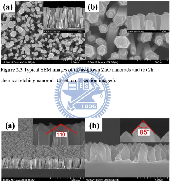
Figure 2.1 The XRD patterns of ZnO seed layer which is annealed at
different temperature……….. 36 Figure 2.2 The SEM images of annealed ZnO seed layer on Si substrate. (a)
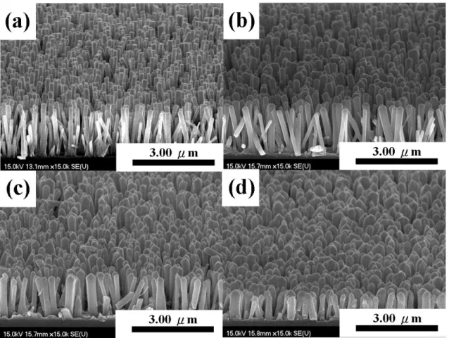
Top and (b) cross view………... 36 Figure 2.3 Typical SEM images of (a) as-grown ZnO nanorods and (b) 2h
chemical etching nanorods (inset: cross section images)………... 37 Figure 2.4 Typical SEM images of (a) the ZnO nanorods after plasma
etching and (b) the ZnO nanorods after two-step etching……….. 37 Figure 2.5 Schematic illustration of the two-step etching process………….. 38 Figure 2.6 Cross section TEM image and EDS spectrum of Si, ZnO seed
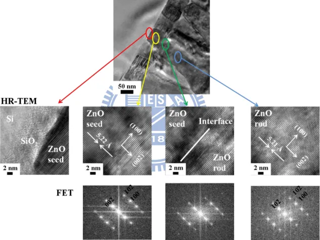
layer, and as-grown ZnO nanorods……… 39 Figure 2.7 HR-TEM images and FET patterns of Si, ZnO seed layer, and
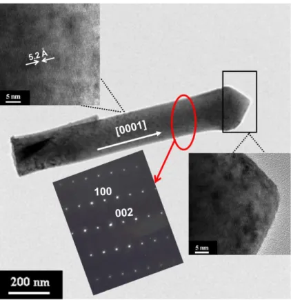
as-grown ZnO nanorods………. 40 Figure 2.8 TEM image of the single ZnO nanorod after plasma etching, the
insets show the corresponding SAED pattern and high resolution
Figure 2.9 (a) J-E curves (inset is F-N plots) and (b) Stability test of the
nanorod emitters………. 42
Chapter 3
Figure 3.1 Typical FE-SEM images of ZnO nanorod with various oxygen plasma treatment times (a) 0 s (as-grown), (b) 30 s, (c) 60 s and (g) 120 s. respectively……….... 51 Figure 3.2 (a) XRD analysis of ZnO nanorod emitters with the various
oxygen plasma eching times. (b) TEM bright field image, corresponding SAED pattern, HR-TEM image and (c) EDS analysis of as-grown ZnO nanorod after 60 s oxygen plasma
etching……… 52 Figure 3.3 Room temperature PL spectra of ZnO nanorod emitters with the
various oxygen plasma etching times (inset show magnify of green emission areas) ……… 53 Figure 3.4 (a) J-E curves and (b) F-N plots of ZnO nanorod emitters with
various oxygen plasma treatment times………. 54 Figure 3.5 Stability at 25 ℃ of ZnO nanorodwith oxygen plasma etching
for 60 s: (a) Turn-on and threshold fields, (b) Field emission enhanced factor, (c) 1st, 100th, 200th and 400th cycle respective J-E curves and (d) FE-SEM images of tip structured ZnO
nanorod emitters for stability tests………. 55 Figure 3.6 Stability at various temperatures of tip structure ZnO nanorod
emitters: (a) J-E curves, (b) Turn-on and threshold fields and (c) Field emission enhancement factor……… 56
Figure 4.1 (a) XRD analysis of ZnO nanorod, nanopagoda, and nanotip emitters. Typical FE-SEM images of (b) nanorod, (c) nanopagoda, and (d) nanotip emitters; (insets of (b), (c) and (d) are their top view images) ………... 65 Figure 4.2 Schematic descriptions of the formations of ZnO nanopagoda
and nanotip emitters………... 66 Figure 4.3 TEM cross section images, corresponding SAED patterns and
HR-TEM images of (a) ZnO nanopagoda and (b) ZnO nanotip
emitters………... 67 Figure 4.4 Room temperature PL spectra of ZnO nanorod, nanopagoda, and
nanotip emitters……….. 68 Figure 4.5 (a) J-E curves (inset shows the F-N plots) of ZnO nanorod,
nanopagoda, and nanotip emitters. (b) Stability at room temperature of ZnO nanopagoda and nanotip emitters………….. 69 Figure 4.6 Stability at various temperatures of ZnO naontip emitters: (a)
J-E curves and (b) turn-on and threshold fields………. 70
Chapter 5
Figure 5.1 Typical FE-SEM images of (a) as-grown ZnO nanowires, (b) ZnO-SnO2-5, (c) ZnO-SnO2-10 and (d) ZnO-SnO2-20 core-shell
nanowires; (insets of (a), (b), (c) and (d): a side images of
as-grown and core-shell nanowires……… 79 Figure 5.2 TEM bright field image, EDS analysis and SAED pattern of the
(a) as-grown ZnO nanowire and (b) ZnO-SnO2-20 core-shell
nanowire………. 80 Figure 5.3 HRTEM images of (a) As-grown ZnO nanowires, (b)
ZnO-SnO2-5, (c) ZnO-SnO2-10 and (d) ZnO-SnO2-20 core-shell
nanowires. ………. 81 Figure 5.4 XPS Spectra of as-grown ZnO and ZnO-SnO2 core-shell
nanowires, (a) Zn spectrum, (b) O spectrum and (c) Sn spectrum 82 Figure 5.5 Dynamic response of (a) as-grown ZnO nanowires, (b)
ZnO-SnO2-5, (c) ZnO-SnO2-10 and (d) ZnO-SnO2-20 core-shell
nanowire sensors at 250 ℃……… 83 Figure 5.6 Plots of sensitivity versus hydrogen concentration at 250 ℃ of
the ZnO-SnO2 core-shell nanowires………... 84
Chapter 6
Figure 6.1 Schematic structure of ZnO nanorod photodetector……….. 94 Figure 6.2 Typical FE-SEM images of (a) ZnO-60, (b) ZnO-30, (b) ZnO-20
and (d) ZnO-10 nanorods, respectively……….. 95 Figure 6.3 (a) XRD patterns and (b) PL spectra of the ZnO nanorods with
various growth times. Inset is the ratios of UV emission to visible light emission as a function of growth time………... 96 Figure 6.4 (a) TEM bright image and (b) EDS analysis of the ZnO-10
nanorod. Inset is the SAED pattern and HRTEM image of the
ZnO-10 nanorod. ………... 97 Figure 6.5 (a) Low magnification SEM image of high bent ZnO-10/PET
structure (b) convex and (c) concave geometric side views and (d) I-V characteristics measured at different bending
morphologies……….. 98 Figure 6.6 UV photodetective properties (a) I-V plot of ZnO-10 nanorods
with power densities of 25, 35 and 70 μW/cm2, respectively. (b) Reversible switching properties of ZnO-10 nanorods. (c) Sensitivity vs time plots under 100 sec illuminations of ZnO nanorods grown with various times at power density of 25 μW/cm2
. (d) Sensitivity vs growth time curves of the nanorods at 0.5 V bias under 100 sec illuminations. (e) Sensitivity vs time plots of longer (ZnO-60) and shorter (ZnO-10) nanorod photodetectors under longer time illumination……….. 99 Figure 6.7 Stability measurements of ZnO-10/ PET photodetector: (a)
different orientation UV illumination (b) retention properites, (c) stability characteristics at UV power density of 25 μW/cm2 and (d) Multilevel photoresponse performed by various UV power density illuminations……….. 100
Chapter 7
Figure 7.1 Schematic structure of the Au/GZO nanorod thin films/ ZnO/Au device structure……….. 113 Figure 7.2 Typical FE-SEM cross sectional images of (a) Device 1, (b)
Device 2, (c) Device 3 and (d) Device 4; (insets of (a)-(d) are top view of the Devices 1, 2, 3, and 4, respectively)………... 114 Figure 7.3 (a) XRD analysis and (b) a-axis and c-axis lattice parameters of
the GZO nanorod thin films with various Ga/Zn molar ratios in
the solutions………... 115 Figure 7.4 (a) TEM bright field image of Device 4 (the inset is EDS
analyzed result of the point indicated) and (b) EDS element line profiles of Device 4……… 116
Figure 7.5 Photoluminescence spectra of the Devices 1, 2, 3, and 4……….. 117 Figure 7.6 (a) and (b) Typical bipolar RS I-V curve of Device 4. (c) The
yield of the Device 2, 3, and 4, respectively……….. 118 Figure 7.7 (a) Pattern size dependence of the resistance value in the ON and
OFF states. (b)-(d) Schematic diagrams of bipolar RS mechanism of GZO nanorod film devices through the formation/rupture of conducting filaments formed between GZO nanorod side wall and ZnO seed layer………... 119 Figure 7.8 Endurance cycle plots of VON and VOFF of Devices (a) 2, (b) 3,
and (c) 4……….. 120 Figure 7.9 Endurance cycle plots of the ON and OFF resistances of Devices
(a) 2, (b) 3, and (c) 4……….. 121 Figure 7.10 Dynamic pulse-induced resistive switching of Device 4.
Applying a -8 V 1μs to switch the memory state to ON state and applying a +6 V 1μs pulse to switch it back to the OFF state…… 122
Chapter 9
Figure 9.1 The illustration of the new ZnO nanotip field emission device…. 128 Figure 9.2 The schematic illustration of the metal oxide/GZO nanorods
double layer RRAM device……… 128 Figure 9.3 The schematic illustration of the single ZnO nanowire device….. 129
Chapter 1
Introduction
1-1. Nanosturcture and nanotechnology
Nanostructures, which are defined with at least on dimension is smaller than one micrometer (μ m), normally between 1-100 nanometer (nm), have been given a lot of attention due to their new physical and chemical properties superior to those of their bulk materials. Figure 1.1 gives a size of nanoscale objects and phenomenon a compared with the size of small everyday objects, feeling for the nano-world in natural [1.1]. Nanotechnology deals with small structures from sub-nanometer to several hundred nanometers. Generally, the nanotechnology is a technology of fabrication and applications of nanomaterials. Nanoscience not only includes fundamental understanding of physical and chemical properties of nanomaterials but also discussion the fundamental relationships between properties, phenomena and dimensions in the nanometer scale. It is widely felt that nanoscience will lead to the next industrial revolution.
Figure 1.2 indicates the nano-dimension and the corresponding density of states of nano and bulk material [1.2]l. Nanomaterials and nanostructures can be defined as zero-dimensional (0D) (nanodots and quantum dots), one-dimensional (1D) (nanowires, nanotubes and nanorods), and two-dimensional (2D) (nanobelts and nanosheets) systems in which at least one dimension is smaller 100 nm.
0D nanomaterials have been extensively studied because of the confinements in all three dimensions. A large number of physical and chemical methods have been developed to fabricate 0D nanomaterials with controlled size and pattern from a rich variety of materials [1.3-1.4]. Many progresses has been made not only in size dependent
physical and chemical properties but also in fabricating devices using 0D nanomaterials as key components, such as sensor, nanodot lasers and biological detectors [1.5-1.7].
1D nanomaterials includes nanowires, nanotubes, nanofibers, and nanorods have attracted much attention [1.8-1.9]. Nanowires and nanorods are the main issues and have attracted marvelous interest over the past years. The nanowire and nanorod provides ideal structures for studying transport processes of one-dimension confined objects and related fundamental phenomena, and they also developing new generation nanodevices with high performance in the future [1.10]. In comparison with 0D and 2D nanomaterials, 1D nanomaterials provide a better model system for investing the dependence of electrical and optoelectronic properties on size reduction and dimensionality. Nanowires and nanorods are a new class of quasi 1D nanomaterials that have been attracting great research interest in the past few years and their superior electrical, mechanical, optical and thermal properties permit them to be used as fundamental building blocks for nanoscale science and technology in fields of electronic devices, such as gas sensor, field emission emitters and photodetector
[1.11-1.13]
.
1-2. ZnO material characteristics
Zinc oxide (ZnO) is a Ⅱ-Ⅵ group semiconductor, has a stable wurtzite structure (P63mc space group) with lattice spacing a=0.325 nm and c=0.521 nm with a c/a ratio of 1.633 as shown in Figure 1.3 [1.8]. It is composed of a number of alternating planes with tetrahedrally-coordinated O2- and Zn2+ ions, stacked alternately along the c- axis. Along the c-axis, the positively charged Zn-(0001) polar surface and negative charged O-(000
ī
) polar surface are the strongest polarity surfaces. The polar surfacescontribute to the variety of ZnO nanostructures by surface reconstruction to maintain a stable structure. ZnO material exhibits high melting temperature (1975℃), high thermal stability and their specific heat is 0.125 cal/gm. ZnO materials with great potential for a variety of practical applications, such as piezoelectric transducers, optical waveguides, surface acoustic wave devices, transparent conductive oxides, chemical sensors, and UV-light emitters [1.14-1.16]. ZnO is a wide direct bandgap (~3.37 eV at room temperature) compound semiconductor that is suitable for photonic applications in the UV or blue spectral range. The high exciton-binding energy (60 meV) allows efficient excitonic emission even at room temperature [1.8]. In addition, ZnO doped with transition metals shows great promise for spintronic applications. It has also been suggested that ZnO exhibits sensitivity to various gas species, namely ethanol (C2H5OH), carbon monoxide (CO) and hydrogen (H2), which makes it
suitable for sensing applications [1.17]. Moreover, it’s piezoelectric (originating from non-centrosymmetric structure) property makes it suitable for electromechanical sensor or actuator applications. The properties of ZnO are listed at Table 1.1 [1.18]. Last but not least, ZnO is a chemically stable and environmentally friendly materials and considerable interest in studying ZnO in the form of powders, single crystals, films, or nanostructures.
A variety of ZnO nanostructure morphologies, such as nanowires [1.19-1.21], nanorods [1.22-1.24], tetrapods [1.25-1.26], and nanoribbons/belts [1.27-1.28], have been reported. ZnO nanostructures have been fabricated by various methods, such as thermal evaporation [1.29-1.32], metal–organic vapor phase epitaxy (MOVPE) [1.33-1.34], laser ablation [1.35-1.36], hydrothermal (aqueous solution) synthesis [1.37-1.40], and template-based synthesis [1.41]. Recently, novel morphologies such as hierarchical nanostructures, bridge-/nail-like nanostructures, tubular nanostructures, nanosheets, nanopropeller arrays, nanohelixes and nano-rings have, amongst others, been
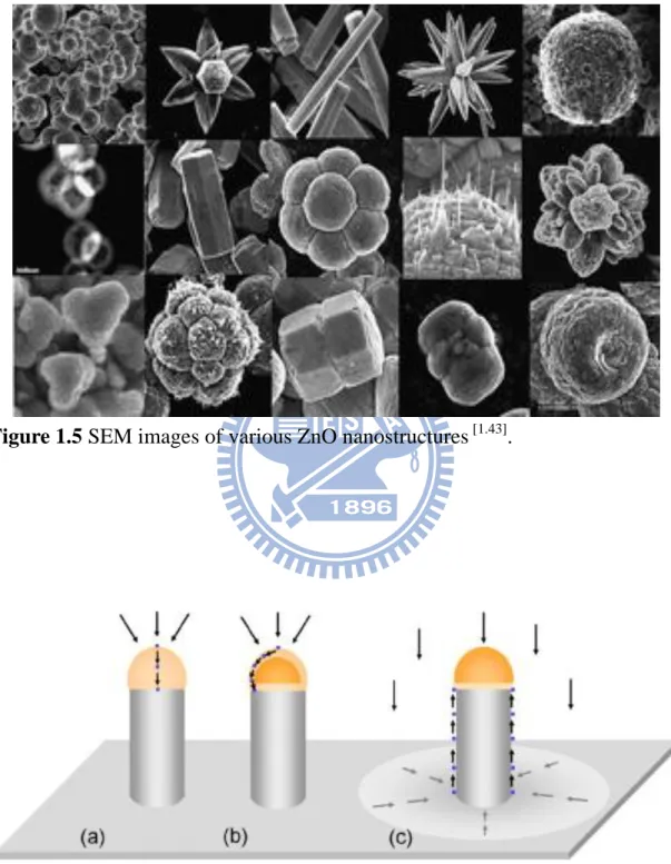
demonstrated. Some of the possible ZnO nanostructure morphologies are shown in Figures 1.4 and 1.5 [1.42-1.43]. The growth and properties of ZnO nanostructures have been extensively studied, but there are still a number of unanswered questions concerning the relationship between fabrication conditions and optical properties.
1-3. Synthesis of zinc oxide nanostructures
ZnO has probably the richest variety of different nanostructures. Its range includes highly ordered nanowires [1.19-1.21], nanorods [1.22-1.24], nanobelts [1.44-1.45], nanotubes [1.46-1.47], nanohelixes [1.48-1.49], and nanorings [1.50-1.51] as shown in Figure 1.4 and 1.5. ZnO nanostructures have been fabricated by various methods, such as thermal evaporation [1.29-1.32], metal-organic vapor phase epitaxy (MOVPE) [1.33-1.34], laser ablation [1.35-1.36], aqueous solution synthesis [1.37-1.40] and electrodeposition
[1.52-1.53]
. Among them, three common growth mechanisms, vapor growth (VLS), aqueous solution growth and electrodeposition, are well established and detail described as follow.
1-3-1 Vapor-liquid-solid method
The VLS growth mechanism was first proposed by Wagner and Ellis in 1964 for Si whisker by hydrogen reduction of SiCl4. The growth mechanism including three
main steps: the formation of the small liquid droplet, nucleation and growth of the nanorods, as shown in Figure 1.6 [1.54-1.55]. In the case of ZnO nanostructures, the thermal evaporation process is realized in a horizontal tube furnace with at least 2 temperature zones. Metal Zn or ZnO powder and graphite are mixed appropriately and load into an alumina boat, and then the boat is placed in the high temperature zone of the furnace under gas flow. As the temperature is increased to the reactive temperature (800-1000 ℃), the ZnO reacts with graphite to form Zn and CO vapor
(equation (1-1)-(1-2)), the gaseous would and condense on the catalyst (low temperature zone) such as Au, Sn and Cu particles [1.56-1.57]. The nucleation is starting and the single crystalline ZnO nanorods grow by the equation (1-3)-(1-4) [1.58-1.59] :
) ( ) ( ) ( ) (s CS Zng COg ZnO (1-1) ) ( 2 ) ( ) ( ) (g ZnOs Zng CO g CO (1-2) ) ( ) ( ) ( ) (g COg ZnOs Cs Zn (1-3) ) ( ) ( 2 ) (s CO g 2COg C (1-4) There are several processing parameters such as temperature, pressure, carrier gas (including gas species and its flow rate), substrate and evaporation time period, which can be controlled and need to be selected properly before and/or during the thermal vaporization [1.60]. The source temperature selection mainly depends on the volatility of the source material. Usually, it is slightly lower than the melting point of the source material. The pressure is determined according to the evaporation rate or vapor pressure of the source material. The substrate temperature usually drops with the distance of its location from the position of the source material. The local temperature determines the type of product that will be obtained. Based on above conditions, the high aspect ratio and large-scale arrays with vertically aligned nanostructure have been produced by this method [1.61].
In additions, some groups have reported combination the VLS and template to synthesis the highly aligned and uniform density ZnO nanorod arrays [1.41, 1.62]. For template materials, anodic aluminum oxide (AAO) is the most popular and highest efficient candidate. The AAO occupied hexagonal ordered porous structure with the porous diameter ranging from 10-200 nm, porous density in the range 1010-1020 /cm2, and high aspect ratio of the channel, which is difficult to achieve with conventional
lithography technology.
1-3-2 Aqueous solution (Hydrothermal) growth method
Aqueous solution growth method is a cheapest method to synthesize ZnO nanorods and has been developed to produce functionalized thin films and coating of metal oxide materials on various substrates, such as single crystalline, polycrystalline and plastic substrates. This method does not require any template or epitaxial substrate to control their orientation and it have many advantages over other growth methods such as low cost, environmental friendliness, catalyst-free, large-scale production and low reaction temperature [1.63-1.65].
The synthesis involves the hydrolysis-condensation of hydrated metal ions and complexes and their heteronuleation onto substrates. Experimentally, the aqueous solution growth simply consists of heating an aqueous solution of metal precursors (salts or complexes) at a given ionic pH, in the presence of substrates at mild temperatures (below 100 ℃). Therefore, such method does not require expensive and complicated equipment. It is entirely recyclable, safe and environmental-friendly, since only water is used as solvent. In addition, since no organic solvents are present, the purity of the as-prepared thin films is substantially improved. The residual salts are easily washed out by water due to their high solubility [1.64].
Verges et al. report the aqueous solution growth method for the first time in 1990
[1.66]
and Greene et al. demonstrated a seeded growth process that was used to synthesize ZnO nanowire arrays in water scale production [1.67]. Recently, there are extensive reports on fabrication of different nanostructures by aqueous solution growth method, such as nanorods [1.38], nanoflowers [1.68], nanoneedles [1.69], nanotubes
[1.70]
, and nanoplates [1.71]. Prevous works of aqueous solution growth were focused on controlling the reaction, concentration of solution, different pH value and synthesis
different morphology. The Table 1.2 summarizes some of aqueous solution growth method and the resulting structures [1.72-1.75]. Based on the above result, the growth solution usually use the zinc nitrate hexahydrate (Zn(NO)3. 6H2O) and the
hexamethylenetetramine (HMT, C6H12N4) in a vessel. The zinc nitrate hexahydrate
which is used as source of zinc and HMT is used to control the pH value. The aqueous solution growth method can be shown in Figure 1.7. These can be represented by the following reactions [1.63, 1.76-1.78]: 3 2 4 6 2) 6 6 4 (CH N H O HCHO NH (1-5) H O NH OH NH3 2 4 (1-6) 2 4 2 ( ) 4OH Zn ZnOH (1-7) OH O H ZnO OH Zn( )24 (s) 2 2 (1-8) The aqueous solution method is based on the formation of solid phase from a solution, which involves two steps about nucleation and growth. In the nucleation, the clusters of molecules are formed undergo rapid decomposition and particles combine to grow up to a certain thickness of the film by heterogeneous reactions on the substrate surface. When zinc nitrate tetrahydrate and HMT are mixed together, no precipitation accrues initially. With the increase of reaction temperature, the HMT begins to decompose into ammonia and the Zn(OH)2 occurs. For the solution is heated,
ZnO nuclei are formed on the substrate. As soon as the ZnO nuclei are formed, the ZnO nanorods begin to grow. This synthesis of ZnO nanorods without catalysts or templates provides a promising option for the large-scale production of well-dispersed one-dimension nanostructure materials.
1-3-3 Electrodeposition growth method
Various groups have used the F-doped SnO2 (FTO), Sn-doped In2O3 (ITO), and Zn
foil substrates to prepare the ZnO nanostructures and by controlling the electrodeposition parameters, such as solution temperature, current density, and deposition time can formation different morphology of ZnO nanostructures [1.79-1.81]. Other groups have reported electrodeposition of thin films and indicate that more positive electrodeposition potentials favor high-quality film growth and additional annealing results in significant enhancement and sharpening of the excitonic emission bands [1.82]. Wong et al. have shown the influence of the substrate surface on the nucleation of nanorods. Electropolishing of Zn foil prior to electrodeposition hinders the nucleation of nanorods. Nonelectropolished films show much narrower and denser growth of ZnO nanorods. The groups conclude that a native surface oxide enhances nucleation [1.81].
In additions, some groups have reported combination the electrodeposition and template to synthesis the uniform density ZnO nanostructures. Liu et al. used electrodeposition and polystyrene (PS) array to synthesis the order-porous ZnO films on Sn-doped In-oxide (ITO) glass substrates and the process. This template is created by self-assembly of an ordered PS array from a suspension of PS spheres and then the ZnO is electrodeposited into the pores of this array. After dissolution of the PS matrix, a stable porous ZnO film is fabricated [1.83]. Le et al. synthesis ordered nanowires uses anodic alumina templates. ZnO nanowires are electrodeposited with diameters of 15-90 nm into the pores of the alumina template and oxidized to ZnO in air at 300 °C
[1.84]
.
1-4. Properties, potential applications of ZnO nanorod arrays
Nannostructures can be defined as systems in which at least one dimension is smaller than 100 nm; that is reducing 1, 2, or 3 dimension (D) of a bulk material to the
nanoscale produces 2D films, 1D nanowires, or 0D nanoclusters, respectively. It well known the dimension of materials continuously shrinks down to nanometer or even smaller scale, some physical properties undergo changes known as the “quantum size effects” [1.85]
. For example, the band gap of ZnO nanoparticles also demonstrates on size dependence. In the past few years, 1D nanostructures materials, such as nanowires, nanorods, nanotube, nanobelts, and nanotip have drawn much attention in basic scientific research and technology applications [1.86-1.90]. In general, the nanorods and nanowires have diameter of 1-200 nm, length of several micrometers with high aspect ratio (length/diameter). Many singular characteristics have been reported including fundamentals of mesoscopic phenomenon and the potential in the buildup of functional electronic [1.91]. In addition, the nanowires and nanorods can provide a material system to experimentally test fundamental quantum mechanical concepts. This section will focus on the physical properties of ZnO nanostructures, including field emission, sensing and resistive switching properties.
1-4-1 Field emission properties
In physics, the characteristic of field emission was first observed by Wood more than one hundred years ago [1.92] and theoretically explained by Fowler and Nordheim in 1928 [1.93]. Generally, the phenomenon of taking electrons from the surface of materials and making them available as free electrons is called as electron emission. The electrons cannot normally escape from the surface of materials at room temperature. The electron field emission depends on a very high electric field at the emission surface. As the electric field at the surface is increased, the potential barrier and the width are reduced. The decrease in barrier width allows the electrons having energy less than electric field at vacuum level to tunnel through (as shown in Figure 1.8). They derived the current-voltage characteristic of field emission process, which
can be written as the follow: heE m e h E e J 3 2 8 2 3 2 3 8 (1-9) where J is the current density (A/cm2), e is the electron charge, E is the electric field (V/cm), h is Plank’s constant, m is the electron mass and φ is the work function (eV) of materials. After that, a modification of the Fowler-Nordheim law to take into account a sharpened emitter-tip shape has been suggested earlier as list in the follow
[1.94-1.97] : ) exp( 2 3 2 2 E B E A J (1-10) E B A E J 2 3 2 2) ln( ) ln( (1-11) 2 3 B Slope (1-12) ) ln( 2 A Intercept (1-13) where β is the field enhancement factor, A (1.56×10⁻¹⁰ AV-2‧eV) and B (6.83×10³ (eV)-3/2V‧μm-1) are constants. In experiment, β could be determined from the slope in plots of ln( 2) E J vs. E 1
when the work function (φ) of material is known as shown in equation (1-12).
The tunneling approach to the electron field emission implies the knowledge of the potential energy barrier to the vacuum. This in turn is essentially determined by the strength of the electric field on the emission tip. For a single nanorod the problem can be modeled by a rounded conductive cylinder immersed in a uniform electric field, that is the single nanorod case:
0 r V E (1-14) where α is conveniently chosen as coefficient. For the case of the nanotubes, the value α=5 is most usual. According the Filip model [1.97]
, when many cylindrical emitters (cathode) are brought together, a neighborhood screening effect appears and the local field on every tip decreases sharply with decreasing distance between the nearest neighbors. In the extreme situation when many emitters (cathode) of equal length are brought into tight contact one actually gets a grounded flat surface facing an anode that is the plane condenser case:
d V
E
(1-15) where d is the cathode-anode gap, V is the cathode voltage. Clearly, the field on the emission sites of real emitters has to be a compromise between those limiting cases. Therefore, V. Filip et al. propose the following phenomenological formula for the strength of the electric field on the cap of a emitter of radius r0 belonging to a
cathode film whose average gap to the anode is d:
d V s r V s E (1 ) 0 (1-16) The screening effect is entirely embedded in the parameter s; whose range is between 0 (for very densely arranged uniformly oriented tubes) and 1 (for a single emitter). Obviously the most realistic values of s for emitters have to be found near 0 since the ratio d=r0 is usually of the order of 1000 and the equation ca simply
formation for the extraction field:
0 F d V E (1-17) where F0 is defined as the apparent field. Nevertheless it should be remembered
that in practice the parameter β is not a characteristic of the emitters but of the entire setup, since it depends on the gap distance d: This fact can be seen from a direct
comparison between equation (1-16) and (1-17): 0 0 1 ) 1 ( 1 r d s r d s (1-18) From the viewpoint of applications, it should be noted that the major requirements for a good field emitter are low turn-on/threshold fields, high current density, high enhancement factor and good reliability. Therefore, in order to get good field emission properties, the emitters should possess a low work function, small dimension of emitter and uniform emitters distribution. In Chapter 2, the plasma etching methods are proposed to control the emitter tip angle to enhance the operating time of the ZnO nanorod emitters.
Generally, two main problems of reliability for the field emission devices are observed, an abrupt variation of turn-on field and a gradual degradation of emission current for a long operating time. These two phenomena might result from different destruction induced from applied electric field or the field emission current. As a speculation, the electrostatic force and the Joule heat generated by high current might be the major factors that degrade the reliably of the field emission properties.
1-4-2 Gas sensor and ultraviolet photodetectors
Oxygen vacancies on metal-oxide surfaces are electrically and chemically active. It is well known that oxygen molecules in an air environment are adsorbed onto the surface of the metal-oxide nanowires to be ionized to O2,
O and O2 ions by
extracting electron from the conduction band of the oxides [1.98-1.100]. The degree of ionization depends on the temperature. O2 is chemisorbed at low temperature
(commonly below 100℃) while O and O2 are chemisorbed at high temperature
(commonly above 100 ℃ ). These vacancies function as n-type donors and significantly increase the conductivity of oxide. When the adsorption of charge
accepting molecules at the vacancy sites, such as NO2 and O2 (oxidation gas),
electrons are effectively depleted from the conduction band, leading to a reduced conductivity of the n-type oxide. On the other hand, molecules, such as H2 (reduction
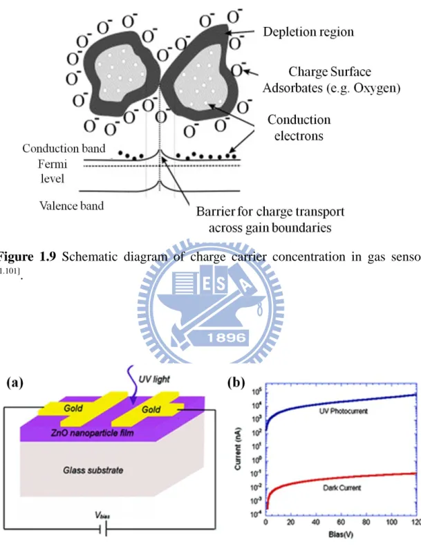
gas), would react with surface adsorbed oxygen and consequently remove it, leading to an increase of conductivity, as shown in Figure 1.9 [1.101].
Most metal-oxide gas sensors operate based on this principle. As one of the major materials for solid state gas sensor, bulk and thin films of ZnO have been proposed for NH3, alcohol and H2 sensing under elevated temperature (~400 °C) [1.102-1.105]
. From the aspect of sensing performance, 1D ZnO nanostructure, such as nanowires and nanorods, is expected to be superior to its thin film counterpart. Since their diameter is small and comparable to the Debye length, chemisorption induced surface states effectively affect the electronic structure of the entire channel, thus confer 1D ZnO nanorods and nanowires have higher sensitivity than thin film.
Ultraviolet (UV) light irradiation of the nanopaticles device of ZnO in air observed to result in a significant increase of the conductivity, as shown in Figure 1.10 [1.106]. These processes could be observed by introducing ON/OFF switch between light source and the ZnO nanostructure as list in the follow:
Initial state ) ( 2 ) ( 2g e O ad O (1-19) Switch ON e h h (1-20) ) ( 2 ) ( 2 ad O g O h (1-21) Switch OFF ) ( 2 ) ( 2g e O ad O (1-22)
Upon illumination, photogenerated holes discharge surface chemisorbed O2
-through surface electron-hole recombination, while the photogenerated electrons significantly increase the conductivity. When illumination is switched off, O2
-molecules re-adsorb onto nanostructure surface and reduce the conductivity. In general, the properties of the photodetector were demonstrated to be improved through nanostructure. Some critical performance parameters of the photodetector are include responsively, photocurrent, recovery time and reliably.
1-4-3 Resistive random access memory (RRAM)
Semiconductor memory has played an important role in the modern electronic devices. It is always a major driver for the development of semiconductor industry during the last few decades. According to the storage property, the modern memory devices are mainly classified into two groups. The first group is the volatile memory (VM), which can hold the stored data only when the system power is supplied. The widely-used VM devices are dynamic access memory (DRAM) and staticrandom access memory (SRAM). The other group is nonvolatile memory (NVM), whose the stored data can be held for a long time without any power supply. For ideal NVM devices, it is expected to possess the properties of low operation voltage, low power consumption, high operation speed, high endurance, long retention time, nondestructive readout, simple structure, small size, and low cost [1.107]. However, there is no NVM device completely including the above properties up to now. Flash memory has been the mainstream of NVM devices nowadays, and it can be divided into the NOR flash and NAND flash. The NOR flash has high operation speed, which is suitable for the computer coding and mobile phone applications. On the other hand, the NAND flash possesses higher density property and is extensively used for the application of the large data storage.
However, the flash memory suffers some severe issues including high operation voltage, high power consumption, and low operation speed. In addition, as the continuous device scaling down, it will meet the physical scaling limitation in the near future, further leading to poor retention time and coupling interference effect [1.108]. Therefore, some modified flash memories, such as charge-trapping (SONOS) flash and band-engineered SONOS flash are proposed to replace the traditional flash memory. Moreover, many researchers are aggressively making their efforts to find the emerging NVM devices with the advantages of DRAM, SRAM, and flash memory. Several high-potential candidates for the next-generation NVM application, including ferroelectric random access memory (FeRAM) [1.109], magnetroresistive random access memory (MRAM) [1.110], phase change random access memory (PCRAM) [1.111], and resistive random access memory (RRAM) have been extensively investigated, respectively. Compared with other NVM, RRAM is based on a large change in electrical resistance between low resistance state (LRS) and high resistance state (LRS) when it is exposed to voltage or current pulses. Both LRS and HRS memory states can be hold for a long time without any power supply and utilized to storage digital data. Table 1.3 illustrates the comparison between DRAM, SRAM, Flash, and the other next-generation NVM candidates [1.107]. As can been seen, RRAM possesses the better advantages, including low operation voltage, low operation power, high operation speed, high scalability, good endurance, and small size, than the other memory devices. As a result, it has been aggressively investigated to replace the present flash memory and extensively considered as the most potential candidate for the next-generation NVM application.
An RRAM device consists of one resistor and one corresponding transistor or diode. The resistor, fabricated in the back-end process, is in the structure of metal/insulator/metal (MIM) with the property of resistance changes for data storage.
During the RRAM operation, applying voltage bias on a thin insulator film (100 nm) sandwiched between two metal electrodes, the electrical characteristics of the MIM device are permanently changed. The device is then said to be formed or electroformed, which is called forming process. Before the resistive switching behavior is observed, forming process, similar to soft dielectric breakdown, is needed to active pristine RRAM devices [1.112-1.113]. This was reported to generate a critical number of point defects, such as oxygen vacancies and metallic defects, in the thin insulator film by applying external electrical signal. These defects will be align to form high leaky paths (conducting filaments) connecting top electrode and bottom electrode [1.114], leading to the reproducible and repeatable resistive switching phenomenon. Therefore, the forming voltage is not only dependent on the thickness of the resistive thin film but also associated its film quality (i.e., defect concentration).
The basic RRAM operational principles, we need to distinguish the relation between the electrical polarity and the resistive switching phenomenon. The switching operation is called unipolar when the switching procedure is dependent on the amplitude of the applied voltage but independent of the voltage polarity. As shown in Figure 1.11, the unipolar switching is switched from HRS to LRS by sweeping voltage bias to the turn-on voltage (i.e., turn-on process), and the current is limited by the current compliance. The resistive switching back to LRS (i.e., turn-off process) takes place at a current higher than current compliance and the amplitude of turn-off voltage is smaller than that of the turn-on voltage. In contrast, the characteristic is called bipolar when the turn-on process occurs at one voltage polarity and the turn-off process at the reversed voltage polarity (Figure 1.12). As shown in Figure 1.13 [1.115], in combination with the unipolar and bipolar switching, the nonploar switching operation is independent of the polarity of the applied voltage and current biases, which both positive and negative voltages can switch its memory state from LRS to
HRS, and vice versa.
1-5. Optical properties of zinc oxide
ZnO generally reveals n-type conduction with a typical carrier concentration of 1017 cm-3, which is smaller than the carrier concentration of 1018 to 1020 cm-3 in ultraviolet light-emitting and laser diode applications. Compared with other direct wide band gap materials, ZnO exhibits a larger exciton binding energy (~60 meV) which assures more efficient exciton emission [1.8]. In addition, the binding energy of ZnO is larger than its thermal energy (~26 meV). For these reasons, ZnO has attracted considerable attention for optical applications such as ultraviolet light-emitting devices and optoelectronic devices. The optical spectrum is shown in Figure1.14 [1.116].
In ZnO, it is noted that the identities of the recombination centers and mechanisms for the luminescence properties are still a matter of controversy. There are two general kinds of emission manners in ZnO. One is the ultraviolet emission (UV emission), and the other is the visible emission. The UV emission is related to the conduction band and valence band of zinc oxide and the visible emission is related to the electron transition from the energy band of impurities and defects (oxygen vacancies) to the valence band. The optical properties of ZnO would be changed by dopant, structure, and annealing [1.117-1.118]. The mechanism of the ultraviolet and visible emission is shown in Figure1.15.
1-6. Outline of dissertation
In the first chapter, the relative backgrounds of this dissertation are introduced briefly including the field emission theory, the sensor theory, and the RRAM devices. Here the motivation and main ideas for the design of our experiment are also described simply.
In the chapter 2-4, the novel methods (plasma etching, chemical etching and two-step aqueous solution growth) are proposed to decrease amount of the oxygen vacancy to enhance the operating time of the ZnO nanotip emitters. The ZnO nanotip emitters have high potential for applications in electron field emission and light emitting devices in the future.
In the chapter 5, the novel spin-coating methods are proposed to prepare SnO2-ZnO core-shell nanostructure to enhance the sensitivity of hydrogen. The
electrical properties of the core-shell nanowires in 0-200 ppm of hydrogen (H2) were
measured at temperature of 250 ℃. The ZnO-SnO2 core-shell nanostructures made by
two-step chemical growth have high potential for gas sensor application.
In chapter 6, the ultra-fast growth method is proposed to prepare short length and uniform ZnO nanorod array on flexible substrate to use in UV photodetector application. Owing to the good performance including mechanical flexibility, nondestructive properties, high reliability and multilevel photoresponse, the well-aligned ZnO nanorods grown on transparent and flexible PET polymer substrates have high potential for UV photodetector applications.
In chapter 7, the ultra-fast growth method is proposed to prepare dense and uniform Ga-ZnO nanorod array on Au/Ti/SiO2/Si substrate to use in RRAM
application. This study also investigates the resistive switching behavior and conduction mechanisms of nanorod thin films without any embedding. Results demonstrate that the films exhibit excellent bipolar resistive switching behavior, including low operation voltage and good endurance property.
Finally, all experimental results in the previous chapters and all the suggested works for futher researches are summarized in chapter 8 and chapter 9, respectively.
Table 1.1 Properties of zinc oxide (ZnO) material [1.18]. Property Value Lattice parameter a0 (300K) 0.32495 nm Lattice parameter c0 (300K) 0.52069 nm Ratio c0/a0 1.633 Density 5.606 g/cm3
Stable phase at 300K Wurtzite (Hexagonal)
Melting point 1975 ℃
Static dielectric constant 8.656
Refractive index 2.008
Energy gap 3.4 eV
Exciton binding energy 60 meV Electron effective mass 0.24 Electron Hall mobility at 300 K for low
n-type conductivity
200 cm2/V‧s Hole effective mass 0.59 Hole Hall mobility at 300 K for low
p-type conductivity
5-50 cm2/V‧s
Table 1.2 Summary of different methods for aqueous solution growth [1.72-1.75]
Growth solution Resulting morphology Focus of investigation Zinc nitrate + HMT Nanorods
Nanotubes
Influence of substrate and seed layer.
Zinc nitrate or zinc acetate + HMT
Highly aligned nanorods Influence of substrate and seed layer. Zinc nitrate + thiourea + ammonium chloride + ammonia Nanowires Tower-like nanowires Flower-like nanowires Tube-like nanowires Influence of growth temperature, reactants and
growth time. Zinc acetate + Sodium hydroxide + Citric acid Disk-like nanorods Flower-like nanorods Nanorods
Influence of reactants and pH value of growth solution.
Table 1.3 The comparison with the Flash memory and next-generation NVM candidates [1.107].
Function DRAM SRAM Flash OUM MRAM RRAM Non-volatility No No Yes Yes Yes Yes
Program power
Low Low High Low High Low
Program voltage
Low Low High Medium Low
Read dynamic margin 100-200 mV 100-200 mV Delta Current 10-100X 20-40 % 10-1000X Write-Erase time 50ns-50ns 8ns-8ns 1μs−1-100 ms 12ns-50ns 30ns-30ns 10ns-30ns Read time 50ns 8ns 50ns 20ns 30ns 20ns Program power
Medium High High Low Medium Low
Multi-bit storage
No No Yes Yes No Yes
Scalability limits
Capacitor 6T T-Ox/HV Litho Current Litho
Endurance ∞ ∞ 1012 >1012 ?1015 ?1015
The Scale of Things-Nanometers
Figure 1.1 The scale of nanoscale [1-1].
Figure 1.2 The dimesionality of confinement and its effects on the density of states [1.2].
Figure 1.3 The wurtzite structure model of ZnO.
Figure 1.5 SEM images of various ZnO nanostructures [1.43].
Figure 1.6 Diffusion models for the source atoms to the growth front of the nanowires: (a) classical VLS with diffusion through a liquid seed, (b) a partially molten particle with liquid surface and interface and solid core and (c) a solid growth seed with a liquid particle wire interface and additional surface diffusion area [1.55].
Figure 1.7Aqueous solution growth mechanisms of ZnO nanorods [1.78].
Figure 1.8 (a) Field emission of electrons from metal or semiconductor surfaces. (b) Band diagram of a semiconductor field-emitter under biasing.
Figure 1.9 Schematic diagram of charge carrier concentration in gas sensor
[1.101].
Figure 1.10 (a) Schematic of a ZnO nanoparticle film device structure. (b) Current versus voltage for a ZnO nanoparticle film device in the dark and under 0.83 mW/cm2 illumination at 370 nm [1.106].
Figure 1.11 The typical I-V curve of unipolar resistive switching. LRS and HRS are switched by applying the same voltage polarity but the amplitude of the turn-off voltage is always smaller than that of the turn-on voltage.
Figure 1.12 The typical I-V curves of bipolar resistive switching. The turn-on process occurs on one voltage polarity while the turn-off process is triggered by the opposite voltage polarity.
Figure 1.13 The typical I-V curve of nonpolar resistive switching. The amplitude of the turn-on voltage is always higher than the voltage at which the turn-off process occurs [1.115].
Figure 1.14 Optical spectrums [1.116].
Chapter 2
Nano Tip Fabrication of Zinc Oxide Nanorods and their
Enhanced Field Emission Properties
2-1. Introduction
One dimensional (1D) ZnO nanomaterials have recently received much attention for their potential applications in field emission displays, solar cells and other nanodevices [2.1-2.3]. So far, among several kinds of fabrication techniques including thermal evaporation, vapor-liquid-solid (VLS) growth [2.4], metal-organic chemical vapor deposition (MOCVD) [2.5] and aqueous solution method [2.6] used for synthesizing 1D ZnO nanomaterials, aqueous solution synthesis has the advantages of low temperature, pressure, simple equipment and ambient being achievable for large area fabrication of different nanosturctures. Efficient electron field emission is one of the unique properties of many low dimensional nanomaterials. Especially, ZnO nanorods have been investigated as electron field emitters due to their high temperature stability, large scale application, high aspect ratio and low working function [2.7-2.11]. The recent field emission analysis result of the 1D ZnO nanomaterials indicates that electrons are more easily emitted from the nanostructures with sharp tips than the nanostructures with a uniform diameter. Therefore, it is necessary to control the morphologies of the nanorods for improving their field emission properties. In this chapter, we fabricate ZnO nanorods by using aqueous solution method and develop a new technique to form ZnO nanotip structure from the as-grown ZnO nanorods by using the chemical etching and plasma etching combination process. Base on the two-step etching process, we could develop
![Table 1.3 The comparison with the Flash memory and next-generation NVM candidates [1.107] .](https://thumb-ap.123doks.com/thumbv2/9libinfo/8030529.161374/41.892.130.768.377.917/table-comparison-flash-memory-generation-nvm-candidates.webp)
![Figure 1.7 Aqueous solution growth mechanisms of ZnO nanorods [1.78] .](https://thumb-ap.123doks.com/thumbv2/9libinfo/8030529.161374/45.892.138.756.239.1062/figure-aqueous-solution-growth-mechanisms-zno-nanorods.webp)