行政院國家科學委員會專題研究計畫 成果報告
子計畫一:新穎光電材料與奈米結構元件光學性質之研究
(2/2)
計畫類別: 整合型計畫
計畫編號:
NSC90-2215-E-002-021-執行期間: 90 年 08 月 01 日至 91 年 09 月 30 日
執行單位: 國立臺灣大學光電工程學研究所
計畫主持人: 詹國禎
共同主持人: 林浩雄
報告類型: 精簡報告
處理方式: 本計畫可公開查詢
中
華
民
國 92 年 5 月 12 日
行政院國家科學委員會專題研究計畫成果報告
新穎光電材料與奈米結構元件之研究(2/2)─
子計畫一:新穎光電材料與奈米結構元件光學性質之研究
計畫編號:NSC 90-2215-E-002-021
執行期限:90 年 8 月 1 日至 91 年 10 月 31 日
主持人:詹國禎 執行機構及單位名稱:台灣大學光電所
共同主持人:林浩雄 執行機構及單位名稱:台灣大學電機系
一、中文摘要
在不同溫度下,以光調制反射率光譜及光激發螢光光譜術量測砷化銦鎵/砷化鎵量子點結構 的光學特性,此量子點結構樣品表面經由場發射電子掃描顯微術及原子力顯微術量測分析,其量 子點面密度約為每平方公分 1×10¹⁰個。在光激發螢光光譜中顯現五個光學躍遷能譜,其中較低 的兩個為量子點內能階躍遷,其次為伴隨形成之超薄量子井的躍遷,最高的兩個能階則為砷化鎵 位障及緩衝層所產生。從溫度與躍遷能值關係可推論,兩個量子點的躍遷能譜的來源應是兩群由 不同銦成分所構成之量子點的最低能態間光學躍遷所造成。 關鍵詞: Abstr actThe optical properties of InGaAs/GaAs quantum dots (QDs) were investigated by temperature-dependent photoluminescence (PL) and photoreflectance (PR) spectroscopies. The surface morphology and structure analysis of InGaAs QDs were also examined and characterized by a field emission scanning electron microscope (SEM) and an atomic force microscope (AFM). The area density of the QDs is on an order of magnitude about 1×10¹⁰ dots/cm2. The PL results exhibited 5 major energy peaks, two of which are attributed to InGaAs QDs, one is attributed to the InGaAs wetting layer and the other two are attributed to GaAs band-gap transitions. Two of the low energy features are identified to the optical transitions of the ground state. They were originated from the two kinds of InGaAs QDs which might be formed with slight change of the indium composition. The results of PR measurements which reveal energy features on the high energy side contributed by GaAs is also reported.
Keywor ds: InGaAs, Quantum dots, Photoluminescence, SEM, AFM
Ⅰ. Introduction
Low dimensional semiconductor systems have been widely studied in many laboratories over the past two decades. These nanostructure materials and devices have attracted considerable attention during the last decade both from fundamental and technological points of view. Self-assembled
the charge carriers and consequently have a discrete energy spectrum with δ-like density of states1-2. These zero-dimensional systems can be employed for quantum device applications such as in lasers3, single electron transistors4, and optical memory structures5, which promise performance improvements of the devices compared to conventional technology. Self-assembled QDs can be formed and derived by strain in highly lattice-mismatched semiconductor materials via heteroepitaxy. The coherent islands appear beyond a critical thickness of the deposited layer during Stranski-Krastanow (SK) strained layer epitaxial growth mode6-8. Many workers have concentrated their efforts on the study of the structureal9-14, optical15-19 and electronic properties20-22 of the InAs/GaAs self-assembled QDs. However, the overall performance of devices has remained inferior to that of quantum wells (QWs) mainly because the size, shape, and composition fluctuation that occur in QDs devices result in a broad photoluminescence (PL) line width of about 40~60 meV at room temperature.
Recently, self-assembled QDs have extended the wavelength range of the InGaAs/GaAs system further into the infrared beyond 1.3 µm15. The InGaAs QDs have also been optimized with uniform, homogeneous and high area densities. High-power semiconductor laser diodes based on multiple InGaAs/GaAs QDs layers grown by metal-organic chemical-vapor deposition (MOCVD) technique are demonstrated3. However, high quality self-assembled QDs via the Stranski-Krastanow growth mode using gas-source molecular beam epitaxy (GS-MBE) still need more work to improve their uniformly in size and shape. The identification of the growth mechanisms that lead to a narrow size distribution is of great importance.
In this work, we report growth method and parameter optimization of InGaAs/GaAs self-assembled QDs, grown by GS-MBE system using migration enhanced epitaxy technique. Optical characterization is carried out by temperature-dependent PL and photoreflectance (PR) spectroscopies. Furthermore, the morphologic and structural analyses are carried out by field emission scanning electron microscopy (SEM) and atomic force microscopy (AFM).
Ⅱ.Exper imental details
The samples were grown by a VG-80H GS-MBE system on n+-GaAs (100) substrates. Samples S1 and S2 were made with migration enhanced epitaxy in a growth order sequence, In-Ga-As and
In-As-Ga-As, respectively. The V/III ratio was 10 and the growth temperature was 500°C. It consists of 500 nm of a GaAs buffer layer followed by 12 periods of GaAs/AlAs short period superlattice (SPS) with a thickness of 2 nm /2 nm, respectively. Then an undoped GaAs epilayer with a thickness of 50 nm is grown. An In0.5Ga0.5As QD layer with a 10 monolayers (MLs) nominal thickness was grown on
top of it and covered by 510 nm of GaAs. In order to examine the morphology and perform the structure analysis, the second InGaAs QDs layer was grown on the top layer.
The morphology structure and surface density analysis of InGaAs QDs on the top layer was performed with a SEM. The height and diameter of the QDs as well as size distribution were roughly measured by AFM on uncapped islands of InGaAs on the top layer. AFM measurements were carried out at ambient environment with a DI (Digital Instrument Inc.) Nanoscope III® AFM (tapping mode).
Photoluminescence measurements were carried out with a 25-mW He-Ne laser at 632 nm and focused on to the sample to a spot size of 1 mm2. The basic PR experimental setup is described in the literature23. The PR measurements were carried out with a 200-Walt halogen-tungsten lamp, which was dispersed by a monochromator to serve as a probe beam. A line of 543.2 nm He-Ne laser with output power of 100 µW was provided as a pumping beam. A mechanical chopper operated at a frequency of 265 Hz to modulate the pumping light. The optical signal of the reflected light from the sample was detected by a liquid-nitrogen-cooled InAs detector.
Ⅲ. Results and discussion
Fig. 1(a) and 1(b) show the SEM images of the InGaAs QDs for samples S1 and S2. The images
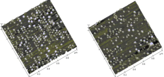
present the uniform QDs and dome (lens-like) QD shape as well as the particle size. The area density of the QDs for S1 and S2 are 2.0x1010 cm-2 and 1.8x1010 cm-2, respectively. The AFM images of samples
S1 and S2 are shown in Fig. 2(a) and 2(b). The average of QD height and base length (diameters) for S1
and S2 are 15 nm × 17 nm and 6 nm × 24 nm, respectively. The area densities of the QDs for S1 and S2
are 4.8×1010 cm-2 and 1.9×1010 cm-2, respectively. However, the area density of QDs is the same order of magnitude (~1.0×1010 cm-2) but the magnitude is a little different. It might be due to the probing of different area of the samples using the SEM and AFM microscopes. The results confirm that the uniformity of QDs on S1 is better than S2, but the size of QD on S1 is larger than S2. It seems to be that
the growth sequential ordering of In-Ga-As could improve better quality of QDs than In-As-Ga-As. The PL spectra of un-etched samples S1 and S2 measured at low temperature (11 K) are shown in
Fig. 3(a). Spectra at same temperature of samples S1 and S2 after etching the top-layer QDs are shown
in Fig. 3(b).
Fig. 1 SEM images of InGaAs/GaAs QDs samples S1(a) and S2(b).
Fig. 2. AFM images of InGaAs/GaAs QDs samples S1(a) and S2(b).
QDs layer.
The energy features on PL for etching and un-etching cases spectra are a little different, but the major energy features are presented on both figures. The optical transitions are labeled by symbols A, B, C, D and E, and marked by arrows on peak positions shown in the figures. Before etching the top-layer QDs of sample S1, the peak energy values EA and EB are 1.15 eV and 1.23 eV, respectively. The
corresponding broadening parameters are 34 meV and 42 meV. After etching, the energy peak values EA and EB are 1.14 eV and 1.22 eV with broadening parameters 27 meV and 46 meV. The results show
that the shape and particle size as well as the transition energy are slightly different. For un-etched sample S2, the energy peak values EA and EB are 1.19 eV and 1.25 eV with corresponding broadening
parameters 23 meV and 51 meV. After etching, the transition energy values EA and EB are 1.19 eV and
1.25eV with corresponding line-width parameters 23 meV and 47 meV. Unlike sample S1, the results of
S2 show that the energy transitions and broadening parameters are almost the same. It means the
growth morphology of the QDs on top layer was less affected by the QDs grown on bottom layer covered with a 510-nm GaAs spacer. The average volume (particle size, height ×diameter2) of the QDs on samples S1 and S2 measured with AFM are roughly to 4.3×10
3
nm3 and 3.5×10³ nm3. Thus the average particle size on sample S1 is larger than that on sample S2. The results also show that transition
energy of S2 is higher than S1. We propose that the EA and EB energy features are attributed to the
optical transition of the ground state of the QDs with two kinds of QDs particle ensembles. The reason will be discussed in following next three paragraphs.
The energy value of the C peak is about 1.40 eV but is not present on sample S1. It is reasonable
and consistent that sample S1 grew with higher average area density and larger average volume of the
QD particles than those of sample S2. The energy feature of the InGaAs wetting layer on InGaAs/GaAs
QD specimens are reported in the literature22. Therefore, the EC peak originates from the wetting layer.
However, the peak disappears on sample S1 due to the larger nano-particles (i.e. QDs). The energy
value of the D and E peaks are about 1.50 eV and 1.52 eV for samples S1 and S2 without or with
etching process. The broadening parameters are different and varied from 4 to 15 meV depending on the sample and etching process. The lower energy peak ED (1.50 eV) is attributed to the buffer layer
and the higher energy peak EE (1.52 eV) originates from the GaAs cap layer. The fitted results are
1.1 1.2 1.3 1.4 1.5 1.6 1.1 1.2 1.3 1.4 1.5 1.6 0.0 0.5 1.0 1.5 E D C B A (b). After Etching S 2 S1 Energy (eV) E D C B A I n te n s it y (a .u .)* 1 0 3 Energy (eV) (a). Before Etching
S 2 S1
summarized and listed in Table 1.
Table 1. Summary of the fitted results from PL spectra at low temperature (11 K). Symbols are denoted with UE (un-etched) and E (etched). The transition energy values in eV and broadening parameters in meV units.
Transition energy features Sample EA ΓA EB ΓB EC ΓC ED ΓD EE ΓE UE 1.15 34 1.23 42 - - 1.50 11 1.52 4 S1 E 1.14 27 1.22 46 - - 1.51 14 - - UE 1.19 23 1.25 51 1.40 8 1.50 11 1.52 6 S2 E 1.19 23 1.25 47 1.40 8 1.50 15 1.52 6
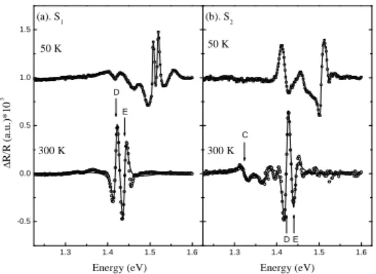
PR spectra carried out at room temperature and low temperature are shown in Fig. 4(a) for sample S1 and Fig. 4(b) for sample S2 .The energy features are fitted by the third derivative function
form (TDFF) with a Lorentzian line shape24. The energy peaks are labeled with the symbols C, D, and E corresponding to Fig. 3 and marked by an arrow notation on the peak position. Two energy values (D, E) fitted by a χ2 fitting method of TDFF Lorentzian line shape are 1.420 (1.423) eV and 1.439 (1.440) eV at room temperature for samples S1 (S2), respectively. The results summary is shown in Table 2.
The energy features (D, E) are attributed to the buffer and cap layers of GaAs. The peak C originates from the InGaAs wetting layer. PR spectra measured at low temperature (50 K) display more energy features which are contributed to the InGaAs wetting layer, GaAs cap and buffer layers. These energy features could not be well fitted to the room-temperature PR spectra. The line shape of PR spectra also changed severely due to temperature cooling down below 50 K. PR spectra might provide more information after detailed line shape analysis which includes strain on GaAs layer. This needs more study in the future.
1.3 1.4 1.5 1.6 1.3 1.4 1.5 1.6 -0.5 0.0 0.5 1.0 1.5 C E D (b). S2 300 K 50 K Energy (eV) E D 50 K Energy (eV) ∆ R /R (a .u .) * 1 0 3 (a). S1 300 K
Fig. 4 PR spectra of InGaAs/GaAs QDs measured at room temperature (300 K) and low temperature (50 K) for samples (a) S1 and (2) S2.
Table 2. Summary of TDFF fitted results from room-temperature PR spectra of un-etched samples S1 and S2. Energy values in eV and broadening parameters in meV units.
EC ΓC ED ΓD EE ΓE
S1 - - 1.420 9 1.439 10
S2 1.326 18 1.423 9 1.440 11
The transition energies measured with PL of low energy portions (EA and EB) are plotted as a
function of temperature for samples S1 and S2 (before etching) are shown in Fig. 5. The trends observed
in EA (InGaAs QDs), EB (InGaAs QDs) and EC (InGaAs wetting layer) are different due to the
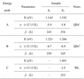
temperature-dependent band-gap of InAs and GaAs materials. Because the wetting layer is an ultra thin InGaAs/GaAs quantum wells, the curve trend on the temperature will follow that of the host material of GaAs. However, the InGaAs QDs will be related to temperature behavior characteristic of the InAs and GaAs materials. The optical properties of the InGaAs QDs and wetting layer were studied with the fitting parameters using Varshni's equation24. The summary of the fitting results are listed in Table 3. The argument of the peak identification was supported by this result. A slight abnormal behavior of the inverted “S-curve” shape on temperature-dependent transition energies measured by PL spectra was observed. It has been explained by the carrier localization on potential minimum of In-rich island24. This effect could be studied by time-resolved PL spectroscopy in the future.
Ⅳ. Conclusion
Temperature-dependent PL and PR experiments were performed and the optical properties ofFig. 5 Transition energies in the low energy portion measured by PL experiments are plotted as a function of temperature.
Table 3. Results summary of the fitted parameters using Varshni’s equation to fit the temperature-dependent transition energy. Sample Energy peak Parameters S1 S2 Notes E (eV) 1.144 1.192 α (×10-4 eV/K) -5.9 -5.8 A β (K) 243 254 QDs1 E (eV) 1.221 1.266 α (×10-4 eV/K) -8.7 -8.9 B β (K) 259 245 QDs2 E (eV) - 1.401 α (×10-4 eV/K) - -3.5 C β (K) - 253 WL
InGaAs/GaAs self-assembled QDs grown by GS-MBE system were studied. Samples of two growth ordering sequences of the adatom, In-Ga-As andIn-As-Ga-As, are explored and characterized with temperature-dependent transition energy spectra and identified two kinds of InGaAs/GaAs QDs ensembles which are originated from two different indium composition fluctuation. The major energy
peaks display on PL and PR spectra were identified and interpreted. An abnormal behavior of the inverted “S-curve” shape presented on temperature-dependent transition energy due to carrier localization were also observed.
References
1. D. Bimberg, M. Grundmann, and N. N. Ledenstov, Quantum Dot Heterostructures (Wiley, Chichester, 1998).
2. Y. Toda, O. Moriwaki, M. Nishioka, and Y. Arakawa, Phys. Rev. Lett. 82, 4114 (1999).
3. F. Heinrichsdorff, Ch. Ribbat, M. Grundmann, and D. Bimberg, Appl. Phys. Lett. 76, 556 (2000). 4. N. Yokoyama, S. Muto, K. Imamura, M. takatsu, T.Mori, Y. Sugiyama, Y. Sakuma, H.Nakao, and T.
Adachihara, Solid State Electron. 40, 505 (1996). 5. G.Yusa and H. Sakaki, Appl. Phys. Lett. 70,345 (1997).
6. I. N. Stranski and L. Krastanow, Akad. Wiss. Lit. Mainz Abh. Math. Naturwiss. K1 IIb 146, 797 (1939).
7. D. Leonard, K. Pond, and P. M. Petroff, Phys. Rev. B 50, 11687 (1994).
8. D. Leonard, M. Krishnamurthy, C. M. Reaves, S. P. Denbaars, and P. M. Petroff, Appl. Phys. Lett.
63, 3203 (1993).
9. L. Goldstein, F. Glas, J. Y. Marzin, M. N. Charasse, and G. Le Roux, Appl. Phys. Lett. 47, 1099 (1985).
10. S. Guha, A. Madhukar, and K. C. Rajkumar, Appl. Phys. Lett. 57, 2110 (1990).
11. J. M. Moison, F. Houzay, F. Barthe, and L. Leprince, E. Andre, and D. Vatel, Appl. Phys. Lett. 64, 196 (1994).
12. A. Tackeuchi, Y. Nakata, S. Muto, Y. Sugiyama, T. Inata, and N. Yokoyama, Jpn. J. Appl. Phys. 34, L 405 (1995).
13. P. B. Joyce, E. C. Le Ru, T. J. Krzyzewski, G. R. Bell, R. Murray, and T. S. Jones, Phys. Rev. B 66, 75316 (2002).
14. A. A. Darhuber, V. Holy, J. Stangl, G. Bauer, A. Krost, F. Heinrichsdroff, M. Grundmann, D.
0 50 100 150 200 250 300 1.05 1.10 1.15 1.20 1.25 1.30 1.35 1.40 Tra nsi ti o n Energ y (eV ) Temperature (K) S1-EA S1-EB S 2-EA S2-EB S2-EC
Bimberg, V. M. Ustinov, P. S. Kop'ev, A. O. Kosogov, and P. Werner, Appl. Phys. Lett. 70, 955 (1997).
15. R. P. Mirin, J. P. Ibbetson, K. Nishi, A. C. Gossard, and J. E. Bowers, Appl. Phys. Lett. 67, 3795 (1995).
16. S. Farfad, R. Leon, D. Leonard, J. L. Merz, and P. M. Petroff, Phys Rev. B 52, 5752 (1995).
17. J. M. Garcia, G. Medeiros-Ribeiro, K. Schmidt, T. Ngo, J. L. Feng, A. Lorke, J. Kotthaus, and P. M. Petroff, Appl. Phys. Lett. 71, 2014 (1997).
18. Q. D. Zhuang, J. M. Li, H. X. Li, Y. P. Zeng, L. Pan, Y. H. Chen, M. Y. Kong, and L. Y. Lin, Appl. Pys. Lett. 73, 3706 (1998).
19. L. Chu, M. Zrenner, M. Bichler, G. Böhm, and G. Abstreiter, Appl. Phys. Lett. 77, 3944 (2000). 20. P. W. Fry, et al, Phys. Rev. Lett. 84, 733 (2000).
21. J. J. Finley, M. Skalitz, M. Arzberger, A. Zrenner, G. Böhm and G. Abstreiter, Appl. Phys. Lett. 73, 2618 (1998).
22. L. Chu, M. Zrenner, G. Böhm, and G. Abstreiter, Appl. Phys. Lett. 76, 1944 (2000).
23. F. H. Pollak, in Handbook on Semiconductors, edited by Balhanski (North-Holland, New York, 1993), Vol. 2.
24. K. L. Teo, J. S. Colton, P. Y. Yu, E. R. Weber, M. F. Li, W. Li, K. Uchida, H. Tokunaga, N. Akutsu, and K. Matsumoto, Appl. Phys. Lett 73, 1697 (1998).