IEEE PHOTONICS TECHNOLOGY LETTERS, VOL. 23, NO. 11, JUNE 1, 2011 691
Efficiency Enhancement in Single-Junction InGaP
Solar Cells by Using Self-Assembled Nanospheres
H. C. Chen, C. C. Lin, H. W. Wang, M. A. Tsai, P. C. Tseng, Y. L. Tsai, H. W. Han, Z. Y. Li, Y. A. Chang,
H. C. Kuo, Senior Member, IEEE, P. Yu, Member, IEEE, and S. H. Lin
Abstract—A single-junction InGaP solar cell with
polysty-rene (PS) nanospheres on the surface has been developed. The self-assembly of PS nanospheres is one of the simplest and the fastest methods with which to build a 2-D closely packed periodic structure. Due to the scattering of the PS nanospheres, the light path length can be increased when compared to the InGaP solar cells without PS nanospheres on the top. An increase short-circuit current from 8.93 to 10.31 mA is improved when a single-junction InGaP solar cell is coated with PS nanospheres. The conversion efficiency measured can also be improved from 8.79% to 9.71%. The single-junction InGaP solar cell with PS nanospheres was achieved.
Index Terms—Angular-reflective spectra, angular-short-circuit
current, InGaP solar cells, self-assembled nanospheres.
I. INTRODUCTION
T
HE III–V compound semiconductor solar cells are promising for high energy conversion efficiency because material’s direct bandgap can yield high internal quantum efficiency. In the past decades, there are numerous III–V solar cell related research results [1], [2] with superior performance. However, the cost issue of III–V solar cells is usually a big concern. We can either reduce the material and processes cost or make the solar cell more efficient to drop the dollar per watt. The highly textured surface has been applied to both silicon and III–V materials [3]–[15] as one of the important methods. Most of the cases were used in silicon cases due to their high per-centages of current solar cell products, while some examples [10]–[14] for III–V materials, which were based on nano-pro-cesses, have shown improvement as well.In this work, we investigate a light harvesting scheme where a scalable and inexpensive bottom-up approach for self-as-sembled 600 nm-diameter polystyrene (PS) nanospheres on
Manuscript received October 14, 2010; revised January 06, 2011; accepted February 19, 2011. Date of publication March 03, 2011; date of current version May 11, 2011. This work was supported in part by the National Science Council in Taiwan under Grant NSC 99-2120-M-006-002.
H. C. Chen, P. C. Tseng, Y. L. Tsai, Z. Y. Li, Y. A. Chang, H. C. Kuo, and P. Yu are with the Department of Photonics and Institute of Electro-Optical En-gineering, National Chiao Tung University, Hsinchu 30010, Taiwan (e-mail: [email protected]; [email protected]).
C. C. Lin and H. W. Han are with the Institute of Photonics System, National Chiao Tung University, Tainan 711, Taiwan (e-mail: chienchunglin@faculty. nctu.edu.tw).
H. W. Wang, M. A. Tsai, and S. H. Lin are with the Department of Elec-trophysics, National Chiao Tung University, Hsinchu 30010, Taiwan (e-mail: [email protected]).
Color versions of one or more of the figures in this letter are available online at http://ieeexplore.ieee.org.
Digital Object Identifier 10.1109/LPT.2011.2122250
single-junction InGaP solar cells is developed. Because of extra scattering of the nanospheres, the path length can be effectively increased. It should be noted that, the self-assembly of nanospheres is one of the simplest and fastest methods to build a 2-D periodic structure. The related characteristics of the single-junction InGaP solar cells with and without utilizing the self-assembly nanospheres are studied. It is found that the nanospheres improve the short-circuit current; hence further the conversion efficiency of the single-junction InGaP solar cell.
II. EXPERIMENTS
The single-junction InGaP solar cell structures were grown by low-pressure (50 Torr) metal-organic chemical vapor deposition in a vertical reactor. A Si doped n-type GaAs sub-strate (100) was used for the subsub-strate. Trimethyl sources of aluminum, gallium and indium were used for group-III precur-sors, while arsine and phosphine were used as the group-V re-action agents. Silane SiH and diethylzinc (DEZn) were used as the n-type and p-type dopant sources, respectively. The V/III ratio was kept about 200 under a growth temperature range of 600–670 C in this work. The photoluminescence peak emission wavelength of InGaP was approximately 655 nm at room tem-perature, and the lattice mismatch between epitaxial InGaP and InAlP layers and GaAs substrate was less than 0.2%.
The InGaP solar cell consists of an -InAlP back-sur-face-field layer [16] to reduce electron-hole recombination, an n-InGaP base layer, a -InGaP emitter layer, a -InAlP window layer, and a -GaAs contact layer to form Ohmic contact with an electrode. The front p-contact consisted of evaporated Ti (250 )/Pt (250 )/Au (5000 ), while Au/Ge (250 )/Au (5000 ) is the bottom n-contact. An anti-reflective coating of SiO film was used for reducing the reflectivity. The PS nanospheres with a plurality of 10 wt% were then spun on the surface. These nanospheres would naturally form into a closely packed hexagonal lattice. A schematic plot of the single-junction InGaP with PS nanospheres solar cell is shown in Fig. 1(a). With properly tuned procedure, the area of the self-assembly closely packed 600 nm diameter PS nanospheres can cover nearly a full 4-inch size wafer as shown in Fig. 1(b). The layout of PS nanospheres with closely packed hexagonal pattern can be seen in Fig. 1(c).
III. RESULTS ANDDISCUSSION
We first measured both transmittance and haze value of PS nanospheres on the glass. The transmittance spectra is scattered between 55% to 70%, and the haze value varies from 58% to 30% in the wavelength range of interest. Considering the difference of substrate (InP versus glass), we believe the results
692 IEEE PHOTONICS TECHNOLOGY LETTERS, VOL. 23, NO. 11, JUNE 1, 2011
Fig. 1. (a) Schematic plot of the fabricate single-junction InGaP solar cell with 600-nm PS nanospheres. (b) Picture of the 4-inch large area self-assembled PS nanospheres. (c) Top view of SEM image of monolayer 600-nm diameter PS.
Fig. 2. Measurement of angular-reflective spectra of single-junction InGaP solar cell (a) with PS and (b) without PS nanospheres.
are satisfactory on the transmission and very good in the haze value. Angular-reflective spectra were achieved by using a broadband Xeon lamp and a custom-built 15 cm-diameter integration sphere. The collected photons were analyzed by a spectrometer. The measured angular-reflective spectra of InGaP solar cell with PS nanospheres and without PS nanospheres were illustrated in Fig. 2(a)–(b), respectively. The InGaP with PS nanospheres dramatically reduced reflectance in the range between nm and 750 nm and the applicable angles of incidence (AOI) up to 60 . We can reasonably state that the PS nanospheres is critical to minimize the Fresnel reflection at the air/solar cell interface. The periodic distribution of nanospheres provided an effective antireflective characteristic, and enhancement of diffracting and scattering incident sunlight on the surface. The enhancement of efficiency can be derived from the increase of [17]:
Where denotes the measured reflectivity, and
the intensity of the AM1.5G solar spectrum. Therefore, the are higher when the reflectance is lower.
The photovoltaic – characteristics were measured under air mass 1.5 global illumination and room temperature con-ditions by a class-A solar simulator with a xenon flash tube of IEC 904–9 standard. Fig. 3 shows the photovoltaic – characteristics of the InGaP solar cell with and without PS
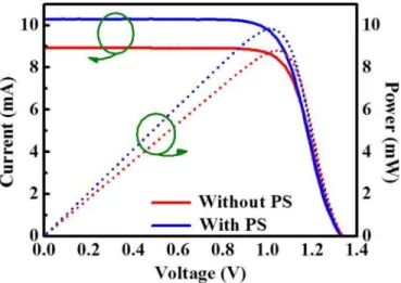
Fig. 3. Photovoltaic – characteristics of the single-junction InGaP solar cell with and without PS nanospheres.
TABLE I
CHARACTERISTICS OF THESINGLE-JUNCTIONInGaP SOLARCELLWITHPS NANOSPHERES ANDWITHOUTPS NANOSPHERES
Fig. 4. External quantum efficiency of the fabricated single-junction InGaP solar cell with and without PS nanospheres. Inset: measured angular dependence of Isc with and without PS nanospheres.
nanospheres. The device characteristics were summarized in Table I. A short-circuit current of 8.93 mA, an open-cir-cuit voltage of 1.33 V and a conversion efficiency of 8.79% are obtained in the InGaP solar cell fabricated by the standard process of without PS nanospheres. For comparison, an of 10.31 mA, an open-circuit voltage of 1.33 V and conversion efficiency of 9.71% are obtained in the solar cell with PS nanospheres. The enhancement factor of the efficiency for the solar cell using self-assembly nanospheres reached 10.47%.
Fig. 4 shows the quantum efficiency of the InGaP solar cell with and without PS nanospheres. It suggests that the periodic
CHEN et al.: EFFICIENCY ENHANCEMENT IN SINGLE-JUNCTION InGaP SOLAR CELLS 693
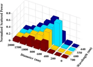
Fig. 5. Simulation of normalized scattered power for different diameters of PS nanospheres.
PS nanospheres provide a better light harvesting effect, and create an efficient light scattering into the InGaP solar cell. Es-pecially, the response in visible spectrum range of 500–700 nm can be very encouraging since most of the sunlight energy is concentrated in this range. While most of the experiments tend to be in normal incidence condition, the direction of sunlight changes every hour during the day. So we need to make sure our PS structure can retain high efficiency insensitive to light inci-dent angle. So an angular short circuit current measurement was performed. This measurement was achieved by using a class-A IEC 904–9 solar simulator with a xenon flash tube. The inset of Fig. 4 shows the angular-short-circuit current of the InGaP solar cell with and without PS nanospheres.
As we shall expect, the periodic PS coated solar cell exhibit drop than the non-PS samples when the sunlight deviates from normal incidence. This result corresponds the previous angular reflectance very well since PS samples showed angle insensitive reflectance much better than non-PS ones’.
Another important issue is to evaluate the effect of diameters of nanospheres. We can calculate the scattering capability by RCWA simulation on scattered power. Then we could normalize the scattered power at wavelength of 440 nm, 500 nm, 600 nm, and 700 nm, respectively. The normalized scattered power was defined in the following ( is the diameter of PS spheres):
From Fig. 5, despite of a peak in 400 nm nanosphere, it shows that 600 nm nanosphere was optimal in a broader wavelength range.
IV. CONCLUSION
In summary, we develop an efficient light harvesting scheme to enhance the efficiency of single-junction InGaP solar cells using self-assembled PS nanospheres. These closely packed monolayer nanospheres are fabricated on the top surface of an InGaP solar cell by spin coating technique. This technique
is suitable for high-throughput, large-area, and inexpensive processing. Due to the extra light scattering, the current-voltage characteristics, external quantum efficiency, and short-circuit current were found to be increased when the PS nanospheres are presented. Finally, an increase conversion efficiency of 10.47% was achieved in the single-junction InGaP solar cell with PS nanospheres.
REFERENCES
[1] R. R. King, D. C. Law, K. M. Edmondson, C. M. Fetzer, G. S. Kinsey, H. Yoon, R. A. Sherif, and N. H. Karam, “40% efficient metamorphic GaInP/GaInAs/Ge multijunction solar cells,” Appl. Phys. Lett., vol. 90, 2007, Article 183576.
[2] S. Wojtczuk, P. Chiu, X. Zhang, D. Derkacs, C. Harris, D. Pulver, and M. Timmons, “InGaP/GaAs/InGaAs 41% concentrator cells using bi-facial epigrowth,” in Proc. IEEE Photovoltaic Specialist Conf., 2010, pp. 0001259–0001264.
[3] J. Zhu, Z. Yu, G. Burkhard, C. M. Hsu, S. Connor, Y. Xu, Q. Wang, M. McGehee, S. Fan, and Y. Cui, “Optical absorption enhancement in amorphous silicon nanowire and nanocone arrays,” Nano Lett., vol. 9, pp. 279–282, 2009.
[4] C. M. Hsu, S. Connor, M. Tang, and Y. Cui, “Wafer-scale silicon nanopillars and nanocones by Langmuir–Blodgett assembly and etching,” Appl. Phys. Lett., vol. 93, 2008, Article 133109.
[5] C. H. Chang, P. Yu, and C. S. Yang, “Broadband and omnidirectional antireflection from conductive indium-tin-oxide nanocolumns pre-pared by glancing-angle deposition with nitrogen,” Appl. Phys. Lett., vol. 94, 2009, Article 051114.
[6] M. Y. Chiu, C. H. Chang, M. A. Tsai, F. Y. Chang, and P. Yu, “Im-proved optical transmission and current matching of a triple-junction solar cell utilizing sub-wavelength structures,” Opt. Express, vol. 18, pp. A308–A313, 2010.
[7] M. Tao, W. Zhou, H. Yang, and L. Chen, “Surface texturing by solution deposition for omnidirectional antireflection,” Appl. Phys. Lett., vol. 91, 2007, Atricle 081118.
[8] M. D. Yang, Y. K. Liu, J. L. Shen, C. H. Wu, C. A. Lin, W. H. Chang, H. H. Wang, H. I. Yeh, W. H. Chan, and W. J. Parak, “Improvement of conversion efficiency for multijunction solar cells by incorporation of Au nanoclusters,” Opt. Express, vol. 16, pp. 15754–15758, 2009. [9] C. Rockstuhl, S. Fahr, F. Lederer, K. Bittkau, T. Beckers, and R. Carius,
“Local versus global absorption in thin-film solar cells with randomly textured surfaces,” Appl. Phys. Lett., vol. 93, 2008, Article 061105. [10] P. Matheu, S. H. Lim, D. Derkacs, C. McPheeters, and E. T. Yu,
“Metal and dielectric nanoparticle scattering for improved optical absorption in photovoltaic devices,” Appl. Phys. Lett., vol. 93, 2008, Article 113108.
[11] Y. A. Chang, Z. Y. Li, H. C. Kuo, T. C. Lu, S. F. Yang, L. W. Lai, L. H. Lai, and S. C. Wang, “Efficiency improvement of single-junction InGaP solar cells fabricated by a novel micro-hole array surface texture process,” Semicond. Sci. Technol., vol. 24, pp. 085007–085010, 2009. [12] I. Prieto, B. Galiana, P. A. Postigo, C. Algora, L. J. Martínez, and I. Rey-Stolle, “Enhanced quantum efficiency of Ge solar cell by a two-di-mensional photonic crystal nanostructured surface,” Appl. Phys. Lett., vol. 94, 2009, Article 191102.
[13] T. H. Chang, P. H. Wu, S. H. Chen, C. H. Chan, C. C. Leel, C. C. Chen, and Y. K. Su, “Efficiency enhancement in GaAs solar cells using self-assembled microspheres,” Opt. Express, vol. 17, pp. 6519–6524, 2009.
[14] P. Yu, C. H. Chang, C. H. Chiu, C. S. Yang, J. C. Yu, H. C. Kuo, S. H. Hsu, and Y. C. Chang, “Efficiency enhancement of GaAs photovoltaics employing antireflective indium tin oxide nanocolumns,” Adv. Mater., vol. 21, pp. 1–4, 2009.
[15] C. P. Chen, P. H. Lin, L. Y. Chen, M. Y. Ke, Y.-W. Cheng, and J. J. Huang, “Nanoparticle-coated n-ZnO/p-Si photodiodes with improved photoresponsivities and acceptance angles for potential solar cell ap-plications,” Nano. Tech., vol. 20, pp. 245204–245209, 2009. [16] J. Nelson, The Physics of Solar Cells. London: Imperial College
Press, 2007, pp. 191–192.
[17] M. A. Tsai, P. C. Tseng, H. C. Chen, H. C. Kuo, and P. Yu, “Enhanced conversion efficiency of a crystalline silicon solar cell with frustum nanorod arrays,” Opt. Express, vol. 19, pp. A28–34, 2011.