High Performance Thin-Film Transistors with Low-High-Low
Band Gap Engineering
Chun-Yen Chang, Yeong-Shyang Lee, Po-Sheng Shih and Chiung-Wei Lin
Department of Electronics Engineering & Institute of Electronics,
National Chiao Tung University, Hsinchu, 300 Taiwan, Republic of China
ABSTRACT
A novel high-performance thin-film transistor (TFT) with low-high-low band gap structure is proposed. We propose a novel device structure combined with low-band-gap materials (microcrystalline Si, tc-Si:H) for the channel region, high-band-gap
materials (hydrogenated amorphous silicon, a-Si:H) for the source and drain offset regions, and heavily doped low-band-gap materials (n a-Si:H) for ohmic contact of source and drain electrodes. We found that, as compared to a-Si:H TFT
device with conventional inverted-stagger structures, the device with low-band-gap materials in the channel (e.g. .tc-Si:H)
which possesses high conductance can effectively improve the film quality of initial growth active layer near the gate
insulator interface and the grown layer. Hence the TFT device parameters such as field effect mobility, threshold voltage,
subthreshold swing and ON-current have been significantly improved. This proposed novel structure with high-band-gap
material is used to prevent the band to band tunneling and alleviate the high OFF-current in conventional .tc-Si:H thin-film
transistors. The proposed high performance TFTs with low-high-low band gap structure will have a great impact in application to high resolution thin-film transistor liquid-crystal displays (TFT-LCDs) and active-matrix liquid-crystal
displays (AMLCDs).
Keywords: thin-film transistor (TFT), Low-High-Low Band Gap Engineering, hydrogenated amorphous silicon (a-Si:H),
microcrystalline Si Q.tc-Si:H) ,polycrystallineSi (Poly-Si)
1. INTRODUCTION
The hydrogenated amorphous silicon thin-film transistors (a-Si:H TFT's) are used as the dominant pixel switching device in
active-matrix liquid-crystal displays (AMLCDs).' However, the most serious problems of present a-Si:H TFTs
development are the low field-effect mobility of carriers and the low reliability in the a-Si:H channel, which lead to a low current drivability and device degradation. Hence, many methods for improving the turn-on characteristics of TFT's device
have been proposed, including through use of a double gate structure,2 short channel device3 or vertical type structure.4 However, All of these technologies are complicated and difficult to perform. On the other hand, polycrystalline silicon (poly-Si) TFT's improve the current drivability while sacrificing the turn-off capability. For reduction of the higher
OFF-state current in poly-Si TFTs, a device using a horizontal offset structure is proposed for reducing the OFF-OFF-state current5.
trapping. However, it needs large device area and other complicated process such as lightly doped implantation, which also
needs higher temperature annealing. Meanwhile, new crystalline materials of higher band mobility than that of a-Si:H (namely microcrystalline silicon; tc-Si:H) is used to perform high-performance TFTs. It is found that j.tc-Si:H TFTs also
have superior current drivabilities. However, the OFF-state current in their proposed devices are still high and produce a low ON/OFF current ratio of only five orders of magnitude or less.69
Previously, we have proposed a high-performance TFT with a novel vertical offset structure, whose channel region and offset region are composed of .tc-Si:H and Si:H films, respectively.'°' Compared to the conventional inverted-stagger
a-Si:H TFTs that consisting ofa single high-band-gap a-a-Si:H layer, the proposed novel TFT is performed with the insertion of
a thin, low-band-gap tc-Si:H layer at the semiconductor/insulator (high-band-gap a-Si:H/SiN) interface. A high quality, low-band-gap .tc-Si:H film is used to enhance the current drivability of this novel device. And, a high-band-gap a-Si:H
layer is used to suppress the OFF-state leakage current toward a value similar to that of conventional a-Si:H TFT's devices. In addition, this novel device use a heavily doped low-band-gap n a-Si:H layer as its source/drain ohmic contacts, resulting in a good ohmic contact between semiconductor and metal.
In this paper, we discuss the dependence of device performance on tc-Si:H channel films with various optical band gaps (E0). Because the fabrication process of the proposed TFTS devices is similar to that used for the conventional inverted-stagger a-Si:H TFTs, the area of our device with low-high-low band gap structure can be reduced to smaller than that a
conventional horizontal offset device. This will increase the pixel density of TFTs array that would be suitable for applying
to future high-definition-television systems (HDTVs). All the films used in our device are deposited of low temperature (
300°C), and the fabrication process is simple and inexpensive with the possibility ofhigh reliability.
2. EXPEIRIMENTAL
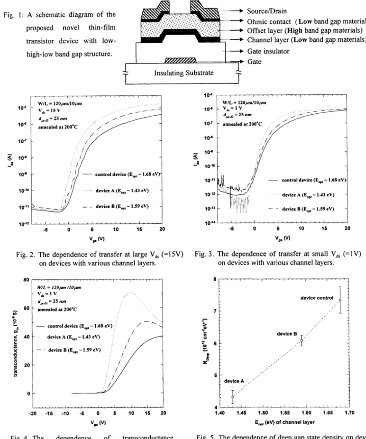
The proposed TFT device with new low-high-low band gap structure is shown schematically in Fig. 1 .The fabrication
process is similar to the conventional inverted-stagger a-Si:H TFT's device except inserting a low-band-gap tc-Si:H film
embedded between the gate insulator and undoped a-Si:H film. First, a 250nm-thick aluminum film is evaporated on silicon
wafers that coated with a 500-nm-thick thermal oxide layer and then patterned to form the gate electrode by
photolithography and wet etching. Secondly, a silicon nitride (SiN) film as the gate insulator, low-band-gap jtc-Si:H and high-band-gap undoped a-Si:H compose the compound channel layer. These along with a low-band-gap n a-Si:H film aredeposited consecutively by a plasma-enhanced chemical vapor deposition (PECVD) system without breaking ofthe vacuum. The gas mixtures for SiNX, undoped a-Si:H and n a-Si:H films are (SiH4 +NH3
+
N2),(SiH4 +H2)and (SiH4 +PH3),and the thickness for SiNX, undoped a-Si:H and n a-Si:H films are 300 nm, 140 nm and 70 nm, respectively. The thickness of tc-Si:H films is fixed at 25nmfor these samples with various [H2]/{[SiH4]+[H2]) flow rate ratio. The SiNX film is deposited under conditions of 300°C, 27.78mw/cm2, and 1 Torr while undoped and n a-Si:H films are deposited at 250°C, 25mw/cm2, 0.3 Torr. In addition, .tc-Si:H films are deposited at 250°C, 25mw/cm2 and 0.55 Torr using a [H2]/{[SiH4J+[H2]} flow rateratio of 980 sccm/(20 sccm +980sccm) for 98%-diluted film and 990 sccm/(10 sccm +990sccm) for 99%-diluted film,
photolithography and wet etching to form source and drain electrodes. Finally, we use CF4 plasma etching to define the active region of the device and to remove the unwanted n a-Si:H layer. The channel width (W) for this device is 120 tm
while the channel length (L) is 1Otm. All the devices were annealed at 200°C in N2 ambient for 25 mm to form good ohmic contacts. The electrical properties of our novel TFTs were measured by a HP4145B semiconductor parameter measurement system with a PC. The crystallinity of tc-Si:H and a-Si:H films is analyzed by Raman scattering spectra. Optical band gap (E0) is determined from a Tauc plot ofthe optical absorption coefficient in —O.4-tm-thick a-Si:H and .tc-Si:H films, which are deposited under identical conditions, except the flow rate of hydrogen and silane gas.
3. RESULTS AND DISCUSSION
In this paper, we discuss the performance of TFT devices with the low-high-low band gap structure compared with that of
control devices without inserting a .tc-Si:H channel layer. The E0 of a-Si:H films prepared with various conditions of
deposition is different. The E0 of undoped a-Si:H film used as the channel layer of control devices is —1 .68 eV, which is
higher than that of 98%-diluted .tc-Si:H films (E0 -1.43 eV) and 99%-diluted .tc-Si:H films (E0, I .59 eV). In addition,
the E0 ofn a-Si:H films used for all devices is -4.48 eV.
Figures 2 and 3 show the transfer curves for devices with jtc-Si:H channel layer of various E0 values, at VdS=l5V and VdSlV, respectively. All the devices have good performances including small threshold voltages and sharp transition regions. As shown in Fig. 2 and Fig. 3, the presence of a low-band-gap tc-Si:H channel layer improves the ON-state
characteristics, and the high-band-gap a-Si:H offset layer suppresses the OFF-state leakage current due to the band-to-band
tunneling (BBT). For convenience of comparison, we denote the devices of 98%-diluted (E0 I .43 eV) and 99%-diluted (E0 1 .59 eV) c-Si:H channel as A and B, respectively. Although the ON-state current of device A is higher than that of device B, the OFF-state current of device A is still lower than that of device B, as shown in Fig. 2 and Fig. 3. Webelieve
that this is dominantly due to the discontinuity of valence band between low-band-gap channel layer and high-band-gap
offset layer. The more higher difference in the valence band discontinuity between low-band-gap channel layer and
high-band-gap offset layer, the more effective hole confinement on suppressing the OFF-state leakage current.'2 The band
discontinuities between low-band-gap channel layer (ic-Si:H) and high-band-gap offset layer (a-Si:H) for devices A and B are —0.25 eV and -O.O9 eV, respectively. Therefore, the effect of suppressing the OFF-state leakage current at device A is noticeable than that at device B. The devices with low-high-low band gap structure reveal higher current driving capabilities than the control device (conventional a-Si:H TFT's). The transconductance g which is defined by 6Ids/6Vgs Vds is fixed' an
important parameter that related to the frequency response. The g 5 proportional to the operating frequency.'3 Fig. 4
demonstrates the dependence of transconductance on gate voltage. The highest transconductance occurs on device A with
98%-diluted tc-Si:H channel, which means that it works very fast. The excess H2 plasma enhances the formation of new
defect, hence the device B with 99%-diluted tc-Si:H channel exhibits a smaller transconductance value than that of device A. However, all the devices with low-band-gap l.tc-Si:H channel work faster than the control device.
From Fig. 2 and Fig. 3, the current density of ON-state is increased from 6.55 mA/rn (control device) to 8.26 mA/rn (device A with 98%-diluted .tc-Si:H channel), then decays to 7.44 mA/m (device B with 99%-diluted llc-Si:H channel). The devices
with low-band-gap tc-Si:H channel can not only improve the OFF-state characteristics but also possess higher driving
currents indeed. The higher ON-current density is due to less bulk trap density. We have measured and deduced the density of deep gap states (Ndeep) accordingthe equation: Ndeep
C1S(qkt)
.Thedensity of deep gap states (Ndeep)of
these devices decreases from 7.34 x 1012 cm2eV (control device) to 6.28 x 1012 cm2eV' (device B with 99%-diluted tc-Si:H channel)then decreases to 4.79 x 1012 cm2eV (device A with 98%-diluted tc-Si:H channel), where S is the subthreshold swing. The
density of deep gap states (Ndeep) 5 dependent on the quality of a-Si:H or ic-Si:H films, and the optical band gap (E0) is
also dependent on the quality of a-Si:H or .tc-Si:H films. Figure 5 demonstrates the dependence of the Ndeep °fl the optical
band gap (E0) ofchannel in devices.
Figure 6(a) demonstrates the variation of subthreshold swing (S) with optical band gap (E0) of channel in devices, which behaves as a trend similar to the density of deep gap states (Ndeep). The subthreshold swing decreases from 1 .0 1 V/dec
(control device with a-Si:H channel whose E0 —1 .68 eV) to 0.96 v/dec (device B with 99%-diluted jtc-Si:H channel whose
E0, -
1.59 eV) then decreases to 0.68 V/dec (device A with 98%-diluted j.tc-Si:H channel whose E0 —1.43 eV). In addition,smaller threshold voltages (Vi) are obtained for our novel devices as shown in Fig. 6(b), in which I .08 V, 1 .65 V and 1.91 V are obtained for A, B and control device, respectively.
Figure 7(a) demonstrates that the performance of devices with low-high-low band gap structure does not degrade by inserting a high quality, low-band-gap .tc-Si:H film. The ON/OFF current ratio increases from 6.19 x jØ5(control device with a-Si:H channel whose E01 —1 .68 eV) to 8.30 x iO (device B with 99%-diluted tc-Si:H channel whose E0 —1.59eV) then increases to 7.30 x 10⁶ (device A with 98%-diluted tc-Si:H channel whose E0 1 .43 eV). Here the ON/OFF current ratio is defined as the ratio of 'ds (01'T)IVgs=20V,Vds=IV to'ds (OFF)IVgs=-IV.Vds=1V Finally, the dependence of the field effect mobility (FE) on optical band gap (E0) of channel layer is shown in Fig. 7(b). The H2 gas dilution method produces high quality jc-Si:H film with less defect centers and lower optical band gap (E0). Hence the density of scattering center which
limit the field mobility is reduced. The speeds ofdevices with low-band-gap tc-Si:H channel are enhanced with higher field effect mobility than the control device of 1 .02 cm2/V-s. Device A (with 98%-diluted .tc-Si:H channel whose E0 -1.43 eV)
has a much higher field effect mobility of2.88 cm2/V-s while 1.64 cm2/V-s for device B (with 99%-diluted tc-Si:H channel
whose E0 1 .59 eV) due to the H2 plasma etching induced damage during the deposition. These field effect mobility are
measured in the saturated region and deduced from the equation: 'ds FECinsW(Vgsth)I'2L. Here riFE, C, is the field effect mobility and gate insulator capacitor respectively.
4. CONCLUSION
A novel high-performance thin-film transistor (TFT) with low-high-low band gap structure, which can be performed easily
under conventional TFT fabrication process, has been proposed and fabricated. A high-band-gap material is embedded vertically between channel and source/drain contacts in this proposed structure. The high-band-gap offset layer, which blocks the carrier conduction at OFF-state of device, is used to prevent the band to band tunneling and alleviate the high OFF-current in conventional thin-film transistors. This proposed structure used low-band-gap material as its channel can improve the device performance, such as current driving capability (ON-state current), field-effect mobility, and so on,
while the high-band-gap material is used to suppress the leakage current due to band to band tunneling (BBT), i.e. gate-induced drain leakage current (GIDL). In addition, this structure used heavily doped low-band-gap material as its source/drain ohmic contacts can obtain the good ohmic contacts between semiconductor and metal. Furthermore, various
materials (for example, VI-VI, IIl-V, Il-VI alloys, and so on) can be widely applied to fabricate the low-band-gap channel,
high-band-gap offset layer, and low-band-gap ohmic contacts for this proposed TFT device with low-high-low band gap
structure.
5. ACKNOWLEDGEMENTS
The authors would like to express their appreciation to the staff of the Semiconductor Research Center, National Chiao Tung University for their technical support. This work was supported by the National Science Council of the Republic of
China under contract No. N5C87-22 1 5-E009-06 1.
6. REFERENCES
1. N. Ibaraki, "Technical issues for 40-inch a-Si:H TFT," AM-LCD '95 Dig., Japan, pp. 67-70, 1995.
2. Y. Kaneko, K. Tsutsui, H. Matsumaru, H. Yamamoto and T. Tsukada, "Amorphous silicon thin film transistor with a buried double-gate structure," IEDM Tech. Dig., pp. 337-340, 1989.
3. Y. Uchida and M. Matsumura, "Short channel a-Si:H thin-film MOS transistor," IEEE Trans. Electron Devices, vol. ED-36, pp. 2940-2943, 1984.
4. Y. Uchida and Y. Nara and M. Matsumura, "Proposed vertical-type amorphous-silicon field-effect transistor," IEEE Electron Device Lett. ,vol.EDL-5,pp. 105- 1 07, 1984.
5. T. Y. Huang, I. W. Wu, A. G. Lewis, A. Chiang and R. H. Bruce, "A simple 100-V polysilicon TFT with improved turn-on characteristics", IEEE Electron Device Lett., vol. EDL-11, pp. 244-246, 1990.
6. S. S. He and G. Lucovsky, "A low temperature plasma-assisted deposition process for microcrystalline thin film transistor, TFTs," Mat. Res. Symp. Proc. ,vol. 336, pp. 25-30, 1994.
7. K. C. Hsu, B. Y. Chen, H. T. Hsu, K. C. Wang, T. R. Yew and H. L. Hwang, "Thin film transistor made from hydrogenated microcrystalline silicon," Japan J. Appl. Phys., vol. 33, pp. 639-642, 1994.
8. C. W. Liang, W. C. Chiang and M. S. Feng, "Microcrystallinityofundoped amorphous silicon film and its effects on the transfer characteristics ofthin-film transistor," Japan I Appl. Phys., vol. 34, pp. 5943-5948, 1995.
9. C. C. Tsai, G. B. Anderson and R. Thompson, "Growth of amorphous, microcrystalline, and epitaxial silicon in low temperature plasma deposition," Mat. Res. Proc., vol. 192, pp. 475-480, 1990.
10. C. Y. Chang and C. W. Lin, "A High-Performance Thin-Film Transistor with a Vertical Offset Structure," IEEE Electron Device Lett., vol. EDL- 1 7, pp. 572-574, 1996.
11. C. Y. Chang and C. W. Lin, "A Novel Thin-Film Transistor with Vertical Offset Structure," Japan J. Appl. Phys., vol. 36, pp. 2032-2043, 1997.
12. P. M. Garone, V. Venkataraman, and J. C. Sturm, "Hole Confinement MOS-gated GexSil-x/Si Heterostructures," IEEE Electron Device Lett., vol. EDL- 12, pp. 230-232, 1991.
Fig. 1: A schematic diagram of the
proposed novel
thin-filmtransistor device with
low-high-low band gap structure.
V• (V)
Fig. 2. The dependence of transfer at large Vd.
(15V)
on devices with various channel layers.
Source/Drain
Ohmic contact ( Low band gap materials) Offset layer (High band gap materials) Channel layer (Low band gap materials)
Gate insulator Gate
V1 (V)
Fig. 3. The dependence of transfer at small VdS
(= lv)
on devices with various channel layers.
-5 0 5 10 15 20 -5 0 5 10 15 20 U) 0
j
4) U C U C 0 U U) C '5 eV) 80 W/L=l2Opnz 110pm Vd, 1 V =25 tim 60 annealed at 200'C— control device (E,, — 1.68 40 . . device A (E,, — 1.43 eV)
— - device B — 1.59 eV) 20 0
/• —
/
I
a) E U0
I
z
8 devIce control 7 device B ••• 6 5 device A . • 4..I
I .40 10 15 20 -20 -15 -10 -6 0 5 V95 (V)Fig.4. The dependence
of
transconductance characteristics on devices with various channel layers.1.45 1.50 1.55 1.60
E, (cv)ofchannel layer
1.65 1.70
Fig. 5.Thedependence of deep gap state density on devices with various E0, values of channel layer.
I .1 device control 1.0 device B . . .. . . . .. . .
i 2
devIce control (I) .. devlceBc0•9
.
. > •D devlceAO.8
:
devlceA .•. I
U) 0.7 • ' 0.6-
0- •
140 1.45 1.50 1.55 1.60 1.65 1.70 1.40 1.45 1.50 1.55 1.60 1.65 1.70(cv) of channel layer E0,, (cv) of channel layer
Fig.6(a). The dependence of subthreshold swing on Fig. 6(b). The dependence of threshold voltage on devices devices with various E0 values of channel with various E0 values ofchannel layer.
layer. iO -1- .. I!
''I'
deviceA'? .
.*
E 0 U.
'_J devlceA .)
2 e:
..
2
deviceB z 0 6 .. .I
.. device control .. . . device control device B 0 1.40 1.45 1.50 1.55 1.60 1.65 1.70 1.40 1.45 1.50 1.55 1.60 1.65 1.70E (cv) of channel layer (eV) of channel layer
Fig.7(a). The dependence of ON/OFF current ratio on